BFP360W
Jun-16-2003
1
NPN Silicon RF Transistor
Preliminary data
Low voltage/ low current operation
For low noise amplifiers
For Oscillators up to 3.5 GHz and Pout > 10 dBm
Low noise figure: 1.0 dB at 1.8 GHz
VPS05605
4
2
1
3
ESD
: Electrostatic discharge sensitive device, observe handling precaution!
Type
Marking
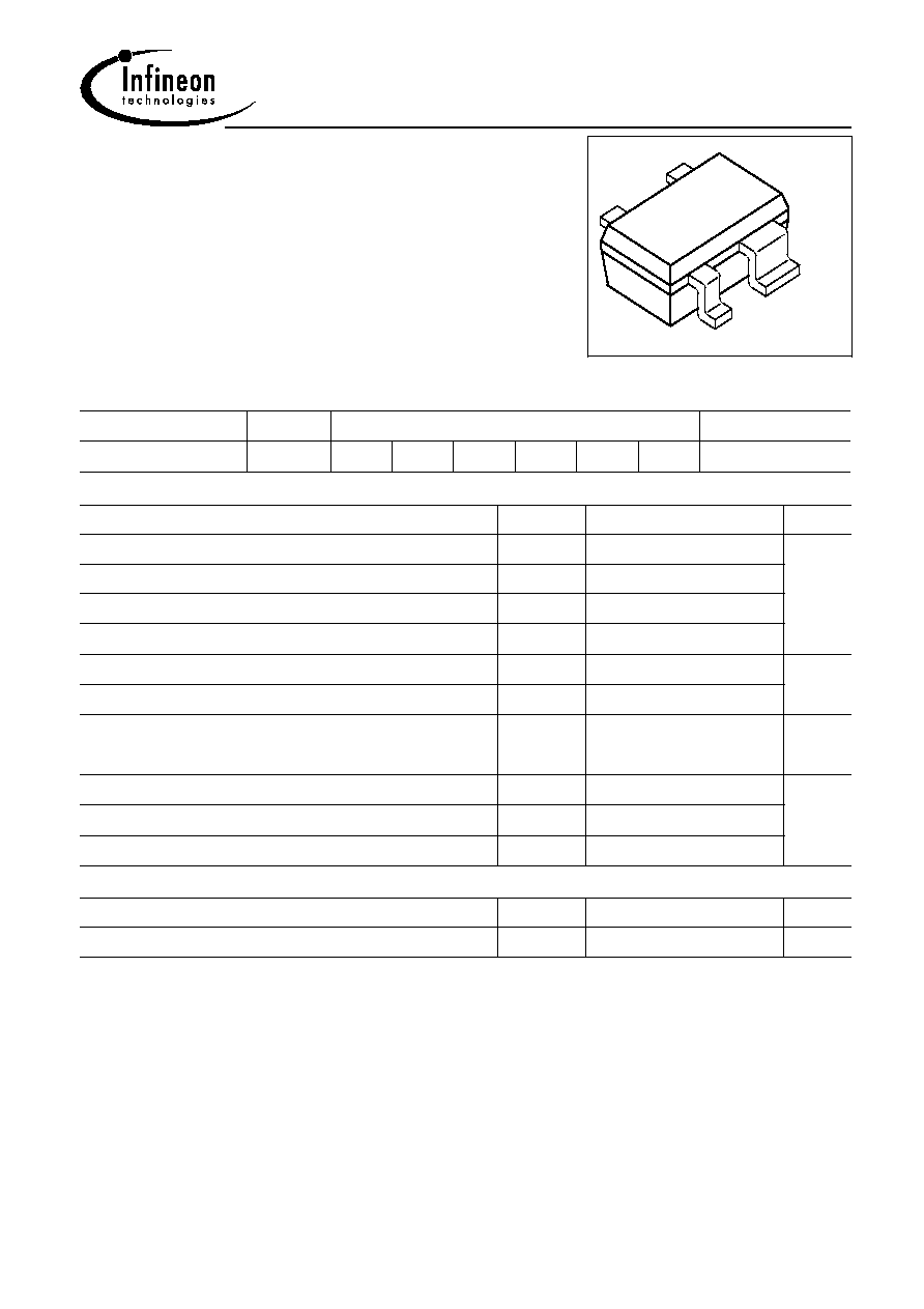
Pin Configuration
Package
BFP360W
FBs
1 = E 2 = C 3 = E 4 = B -
-
SOT343
Maximum Ratings
Parameter
Symbol
Value
Unit
Collector-emitter voltage
V
CEO
6
V
Collector-emitter voltage
V
CES
15
Collector-base voltage
V
CBO
15
Emitter-base voltage
V
EBO
2
Collector current
I
C
35
mA
Base current
I
B
4
Total power dissipation
1)
T
S
95�C
P
tot
210
mW
Junction temperature
T
j
150
�C
Ambient temperature
T
A
-65 ... 150
Storage temperature
T
stg
-65 ... 150
Thermal Resistance
Parameter
Symbol
Value
Unit
Junction - soldering point
2)
R
thJS
260
K/W
1TS is measured on the collector lead at the soldering point to the pcb
2For calculation of R
thJA
please refer to Application Note Thermal Resistance

BFP360W
Jun-16-2003
2
Electrical Characteristics
at T
A
= 25�C, unless otherwise specified
Parameter
Symbol
Values
Unit
min.
typ.
max.
DC Characteristics
Collector-emitter breakdown voltage
I
C
= 1 mA, I
B
= 0
V
(BR)CEO
6
9
-
V
Collector-emitter cutoff current
V
CE
= 15 V, V
BE
= 0
I
CES
-
-
10
�A
Collector-base cutoff current
V
CB
= 5 V, I
E
= 0
I
CBO
-
-
100
nA
Emitter-base cutoff current
V
EB
= 1 V, I
C
= 0
I
EBO
-
-
1
�A
DC current gain
I
C
= 15 mA, V
CE
= 3 V
h
FE
60
130
200
-

BFP360W
Jun-16-2003
3
Electrical Characteristics
at T
A
= 25�C, unless otherwise specified
Parameter
Symbol
Values
Unit
min.
typ.
max.
AC Characteristics
(verified by random sampling)
Transition frequency
I
C
= 15 mA, V
CE
= 3 V, f = 1 GHz
f
T
11
14
-
GHz
Collector-base capacitance
V
CB
= 5 V, f = 1 MHz, emitter grounded
C
cb
-
0.3
0.5
pF
Collector emitter capacitance
V
CE
= 5 V, f = 1 MHz, base grounded
C
ce
-
0.28
-
Emitter-base capacitance
V
EB
= 0.5 V, f = 1 MHz, collector grounded
C
eb
-
0.47
-
Noise figure
I
C
= 3 mA, V
CE
= 3 V, Z
S
= Z
Sopt
,
f
= 1.8 GHz
F
min
-
1
-
dB
Power gain, maximum stable
1)
I
C
= 15 mA, V
CE
= 3 V, Z
S
= Z
Sopt
,
Z
L
= Z
Lopt
, f = 1.8 GHz
G
ms
-
17.5
-
dB
Power gain, maximum available
1)
I
C
= 15 mA, V
CE
= 3 V, Z
S
= Z
Sopt
,
Z
L
= Z
Lopt
, f = 3 GHz
G
ma
-
12
-
dB
Transducer gain
I
C
= 15 mA, V
CE
= 3 V, Z
S
= Z
L
= 50
,
f
= 1.8 GHz
I
C
= 15 mA, V
CE
= 3 V, Z
S
= Z
L
= 50
,
f
= 3 GHz
|S
21e
|
2
-
-
14
9.5
-
-
dB
Third order intercept point at output
2)
V
CE
= 3 V, I
C
= 15 mA, f = 1.8 GHz,
Z
S
= Z
L
= 50
IP
3
-
24
-
dBm
1dB Compression point at output
I
C
= 15 mA, V
CE
= 3 V, Z
S
= Z
L
= 50,
f
= 1.8 GHz
P
-1dB
-
9
-
1G
ms
= |S
21e
/S
12e
|, G
ma
= |S
21e
/ S
12e
| (k-(k�-1)
1/2
)
2IP3 value depends on termination of all intermodulation frequency components.
Termination used for this measurement is 50
from 0.1 MHz to 6 GHz
BFP360W
Jun-16-2003
4
SPICE Parameter (Gummel-Poon Model, Berkley-SPICE 2G.6 Syntax):
Transitor Chip Data:
IS =
0.0689
fA
VAF =
20
V
NE =
2.4
-
VAR =
60
V
NC =
1.4
-
RBM =
7.31
CJE =
400
fF
TF =
9.219
ps
ITF =
1.336
mA
VJC =
0.864
V
TR =
1.92
ns
MJS =
0
-
XTI =
0
-
AF =
1
-
BF =
147
-
IKF =
77.28
mA
BR =
6
-
IKR =
0.3
A
RB =
0.1
RE =
78.2
m
VJE =
1.3
V
XTF =
0.115
-
PTF =
0
deg
MJC =
0.486
-
CJS =
0
fF
XTB =
0
-
FC =
0.954
KF =
1E-14
-
NF =
1
-
ISE =
150
fA
NR =
1
-
ISC =
20
fA
IRB =
74
�A
RC =
0.35
MJE =
0.5
-
VTF =
0.198
V
CJC =
473
fF
XCJC =
0.129
-
VJS =
0.75
V
EG =
1.11
eV
NK =
0.5
K
All parameters are ready to use, no scalling is necessary.
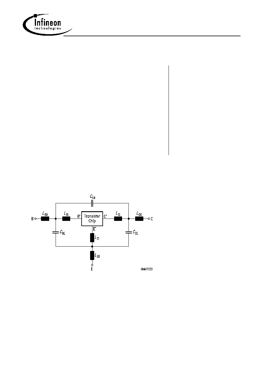
Package Equivalent Circuit:
L
BI
=
0.43
nH
L
BO
=
0.47
nH
L
EI
=
0.26
nH
L
EO
=
0.12
nH
L
CI
=
0.06
nH
L
CO
=
0.36
nH
C
BE
=
68
fF
C
CB
=
46
fF
C
CE
=
232
fF
For examples and ready to use parameters
please contact your local Infineon Technologies
distributor or sales office to obtain a Infineon
Technologies CD-ROM or see Internet:
http//www.infineon.com/silicondiscretes
Valid up to 6GHz