
BFP420
SIEGET
25
Aug-20-2001
1
NPN Silicon RF Transistor
For high gain low noise amplifiers
For oscillators up to 10 GHz
Noise figure F = 1.1 dB at 1.8 GHz
outstanding G
ms
= 21 dB at 1.8 GHz
Transition frequency f
T
= 25 GHz
Gold metallization for high reliability
SIEGET
25 GHz f
T
- Line
VPS05605
4
2
1
3
ESD
: Electrostatic discharge sensitive device, observe handling precaution!
Type
Marking
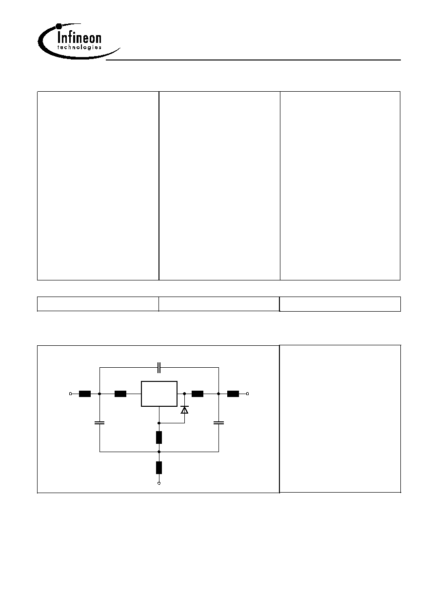
Pin Configuration
Package
BFP420
AMs
1 = B
2 = E
3 = C
4 = E
SOT343
Maximum Ratings
Parameter
Symbol
Value
Unit
Collector-emitter voltage
V
CEO
4.5
V
Collector-base voltage
V
CBO
15
Emitter-base voltage
V
EBO
1.5
Collector current
I
C
35
mA
Base current
I
B
3
Total power dissipation
T
S
107�C
1)
P
tot
160
mW
Junction temperature
T
j
150
�C
Ambient temperature
T
A
-65 ... 150
Storage temperature
T
stg
-65 ... 150
Thermal Resistance
Junction - soldering point
2)
R
thJS
260
K/W
1T
S
is measured on the emitter lead at the soldering point to the pcb
2For calculation of R
thJA
please refer to Application Note Thermal Resistance

BFP420
SIEGET
25
Aug-20-2001
2
Electrical Characteristics at T
A
= 25�C, unless otherwise specified.
Parameter
Symbol
Values
Unit
min.
typ.
max.
DC characteristics
Collector-emitter breakdown voltage
I
C
= 1 mA, I
B
= 0
V
(BR)CEO
4.5
5
-
V
Collector-base cutoff current
V
CB
= 5 V, I
E
= 0
I
CBO
-
-
200
nA
Emitter-base cutoff current
V
EB
= 1.5 V, I
C
= 0
I
EBO
-
-
35
�A
DC current gain
I
C
= 20 mA, V
CE
= 4 V
h
FE
50
100
150
-
AC characteristics (verified by random sampling)
Transition frequency
I
C
= 30 mA, V
CE
= 3 V, f = 2 GHz
f
T
18
25
-
GHz
Collector-base capacitance
V
CB
= 2 V, f = 1 MHz
C
cb
-
0.15
0.3
pF
Collector-emitter capacitance
V
CE
= 2 V, f = 1 MHz
C
ce
-
0.37
-
Emitter-base capacitance
V
EB
= 0.5 V, f = 1 MHz
C
eb
-
0.55
-
Noise figure
I
C
= 5 mA, V
CE
= 2 V, Z
S
= Z
Sopt
,
f
= 1.8 GHz
F
-
1.1
-
dB
Power gain, maximum stable
1)
I
C
= 20 mA, V
CE
= 2 V, Z
S
= Z
Sopt
, Z
L
= Z
Lopt
,
f
= 1.8 GHz
G
ms
-
21
-
Insertion power gain
I
C
= 20 mA, V
CE
= 2 V, f = 1.8 GHz,
Z
S
= Z
L
= 50
|S
21
|
2
14
17
-
Third order intercept point
I
C
= 20 mA, V
CE
= 2 V, Z
S
=Z
Sopt
, Z
L
=Z
Lopt
,
f
= 1.8 GHz
IP
3
-
22
-
dBm
1dB Compression point
I
C
= 20 mA, V
CE
= 2 V, f = 1.8 GHz,
Z
S
=Z
Sopt
, Z
L
=Z
Lopt
P
-1dB
-
12
-
1
G
ms
= |S
21
/ S
12
|
BFP420
SIEGET
25
Aug-20-2001
3
SPICE Parameters (Gummel-Poon Model, Berkley-SPICE 2G.6 Syntax) :
Transistor Chip Data
IS =
0.20045
fA
VAF =
28.383
V
NE =
2.0518
-
VAR =
19.705
V
NC =
1.1724
-
RBM =
3.4849
CJE =
1.8063
fF
TF =
6.7661
ps
ITF =
1
mA
VJC =
0.81969
V
TR =
2.3249
ns
MJS =
0
-
XTI =
3
-
BF =
72.534
-
IKF =
0.48731
A
BR =
7.8287
-
IKR =
0.69141
A
RB =
8.5757
RE =
0.31111
VJE =
0.8051
V
XTF =
0.42199
-
PTF =
0
deg
MJC =
0.30232
-
CJS =
0
F
XTB =
0
-
FC =
0.73234
-
NF =
1.2432
-
ISE =
19.049
fA
NR =
1.3325
-
ISC =
0.019237
fA
IRB =
0.72983
mA
RC =
0.10105
MJE =
0.46576
-
VTF =
0.23794
V
CJC =
234.53
fF
XCJC =
0.3
-
VJS =
0.75
V
EG =
1.11
eV
TNOM
300
K
C'-E'-Diode Data (Berkley-SPICE 2G.6 Syntax) :
IS =
3.5
fA
RS =
10
N =
1.02
-
All parameters are ready to use, no scaling is necessary
Package Equivalent Circuit:
L
BI
=
0.47
nH
L
BO
=
0.53
nH
L
EI
=
0.23
nH
L
EO
=
0.05
nH
L
CI
=
0.56
nH
L
CO
=
0.58
nH
C
BE
=
136
fF
C
CB
=
6.9
fF
C
CE
=
134
fF
EHA07389
L
BI
BE
C
BO
L
C
EI
L
L
EO
CB
C
CI
L
CO
L
CE
C
Transistor
C'-E'-
B
Diode
E
E'
C'
B'
Chip
Valid up to 6GHz
The SOT-343 package has two emitter leads. To avoid high complexity of the package equivalent circuit,
both leads are combined in one electrical connection.
Extracted on behalf of Infineon Technologies AG by:
Institut f�r Mobil-und Satellitentechnik (IMST)
For examples and ready to use parameters please contact your local Infineon Technologies
distributor or sales office to obtain a Infineon Technologies CD-ROM or see Internet:
http://www.infineon.com/silicondiscretes
BFP420
SIEGET
25
Aug-20-2001
4
For non-linear simulation:
Use transistor chip parameters in Berkeley SPICE 2G.6 syntax for all simulators.
If you need simulation of the reverse characteristics, add the diode with the
C'-E'- diode data between collector and emitter.
Simulation of package is not necessary for frequencies < 100MHz.
For higher frequencies add the wiring of package equivalent circuit around the
non-linear transistor and diode model.
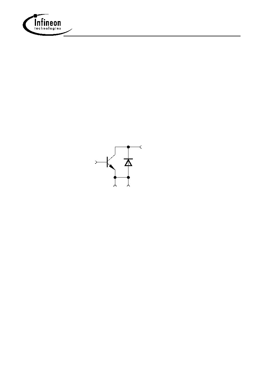
Note:
This transistor is constructed in a common emitter configuration. This feature causes
an additional reverse biased diode between emitter and collector, which does not
effect normal operation.
EHA07307
C
E
E
B
Transistor Schematic Diagram
The common emitter configuration shows the following advantages:
Higher gain because of lower emitter inductance.
Power is dissipated via the grounded emitter leads, because the chip is mounted
on copper emitter leadframe.
Please note, that the broadest lead is the emitter lead.
Common Emitter S- and Noise-parameter
For detailed S- and Noise-parameters please contact your local Infineon Technologies
distributor or sales office to obtain a Infineon Technologies Application Notes
CD-ROM or see Internet: http://www.infineon.com/silicondiscretes
BFP420
SIEGET
25
Aug-20-2001
5
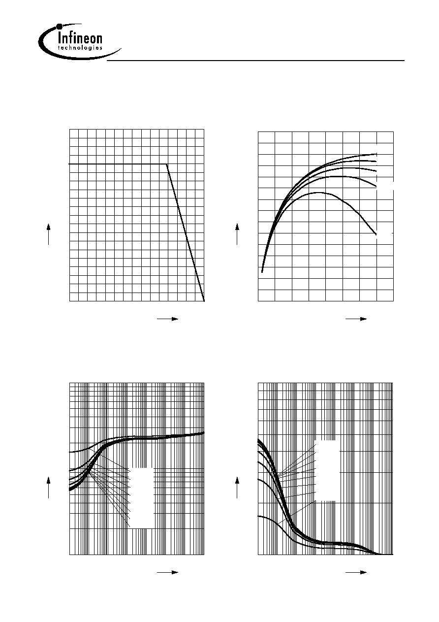
Total power dissipation P
tot
= f (T
S
)
0
20
40
60
80
100
120 �C
150
T
S
0
20
40
60
80
100
120
140
160
mW
200
P
tot
Transition frequency
f
T
= f (I
C
)
f
= 2 GHz
V
CE
= parameter in V
0
5
10
15
20
25
30
mA
40
I
C
0
2
4
6
8
10
12
14
16
18
20
22
24
GHz
30
f
T
2 to 4
1.5
1
0.75
0.5
Permissible Pulse Load
P
totmax
/P
totDC
= f (t
p
)
10
-7
10
-6
10
-5
10
-4
10
-3
10
-2
10
0
s
t
p
0
10
1
10
-
P
totmax
/ P
tot
D
C
D = 0
0.005
0.01
0.02
0.05
0.1
0.2
0.5
Permissible Pulse Load R
thJS
= f (t
p
)
10
-7
10
-6
10
-5
10
-4
10
-3
10
-2
10
0
s
t
p
1
10
2
10
3
10
K/W
R
thJS
0.5
0.2
0.1
0.05
0.02
0.01
0.005
D = 0