BFP460
Jun-14-2004
1
NPN Silicon RF Transistor*
∑
For low voltage / low current applications
∑
Ideal for VCO modules and low noise amplifiers
∑
Low noise figure: 1.1 dB at 1.8 GHz
∑
Excellent ESD performance
∑
High f
T
of 22 GHz
* Short-term description
VPS05605
4
2
1
3
ESD: Electrostatic discharge sensitive device, observe handling precaution!
Type
Marking
Pin Configuration
Package
BFP460
ABs
1 = E 2 = C 3 = E 4=B
-
-
SOT343
Maximum Ratings
Parameter
Symbol
Value
Unit
Collector-emitter voltage
T
A
> 0 ∞C
T
A
0 ∞C
V
CEO
4.5
4.2
V
Collector-emitter voltage
V
CES
15
Collector-base voltage
V
CBO
15
Emitter-base voltage
V
EBO
1.5
Collector current
I
C
50
mA
Base current
I
B
5
Total power dissipation
1)2)
T
S
100∞C
P
tot
200
mW
Junction temperature
T
j
150
∞C
Ambient temperature
T
A
-65 ... 150
Storage temperature
T
stg
-65 ... 150
Thermal Resistance
Parameter
Symbol
Value
Unit
Junction - soldering point
3)
R
thJS
250
K/W
1P
tot
due to Maximum Ratings
2TS is measured on the collector lead at the soldering point to the pcb
3For calculation of R
thJA
please refer to Application Note Thermal Resistance

BFP460
Jun-14-2004
2
Electrical Characteristics at T
A
= 25∞C, unless otherwise specified
Parameter
Symbol
Values
Unit
min.
typ.
max.
DC Characteristics
Collector-emitter breakdown voltage
I
C
= 1 mA, I
B
= 0
V
(BR)CEO
4.5
5.8
-
V
Collector-base cutoff current
V
CB
= 5 V, I
E
= 0
I
CBO
-
-
100
nA
Emitter-base cutoff current
V
EB
= 0,5 V, I
C
= 0
I
EBO
-
-
1
µA
DC current gain
I
C
= 20 mA, V
CE
= 3 V, pulse measured
h
FE
90
120
160
-

BFP460
Jun-14-2004
3
Electrical Characteristics at T
A
= 25∞C, unless otherwise specified
Parameter
Symbol
Values
Unit
min.
typ.
max.
AC Characteristics (verified by random sampling)
Transition frequency
I
C
= 30 mA, V
CE
= 3 V, f = 1 GHz
f
T
16
22
-
GHz
Collector-base capacitance
V
CB
= 3 V, f = 1 MHz, emitter grounded
C
cb
-
0.32
0.45 pF
Collector emitter capacitance
V
CE
= 3 V, f = 1 MHz, base grounded
C
ce
-
0.28
-
Emitter-base capacitance
V
EB
= 0.5 V, f = 1 MHz, collector grounded
C
eb
-
0.55
-
Noise figure
I
C
= 5 mA, V
CE
= 3 V, Z
S
= Z
Sopt
,
f = 1.8 GHz
I
C
= 5 mA, V
CE
= 3 V, Z
S
= Z
Sopt
,
f = 3 GHz
F
-
-
1.1
1.35
-
-
dB
Power gain, maximum stable
1)
I
C
= 20 mA, V
CE
= 3 V, Z
S
= Z
Sopt
,
Z
L
= Z
Lopt
, f = 1.8 GHz
G
ms
-
17.5
-
dB
Power gain, maximum available
1)
I
C
= 20 mA, V
CE
= 3 V, Z
S
= Z
Sopt
,
Z
L
= Z
Lopt
, f = 3 GHz
G
ma
-
12.5
-
dB
Transducer gain
I
C
= 20 mA, V
CE
= 3 V, Z
S
= Z
L
= 50
,
f = 1,8 GHz
I
C
= 20 mA, V
CE
= 3 V, Z
S
= Z
L
= 50
,
f = 3 GHz
|S
21e
|
2
-
-
15
10.5
-
-
dB
Third order intercept point at output
2)
V
CE
= 3 V, I
C
= 20 mA, f = 1.8 GHz
IP
3
-
27.5
-
dBm
1dB Compression point at output
I
C
= 20 mA, V
CE
= 3 V, f = 1.8 GHz
P
-1dB
-
11.5
-
1G
ma
= |
S
21
/
S
12
| (k-(k≤-1)
1/2
),
G
ms
=
S
21
/
S
12
2IP3 value depends on termination of all intermodulation frequency components.
Termination used for this measurement is 50
from 0.1 MHz to 6 GHz
BFP460
Jun-14-2004
4
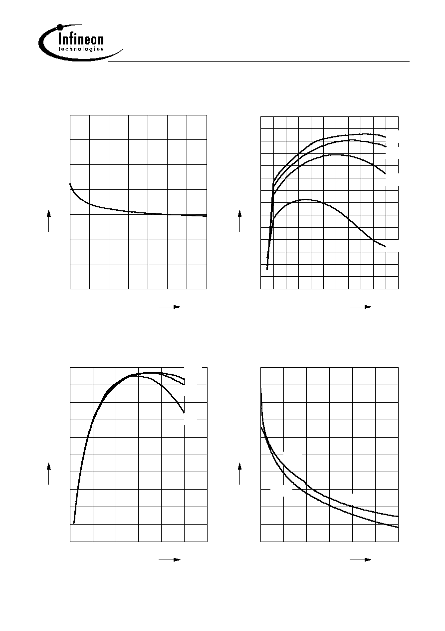
Collector-base capacitance C
cb
=
(V
CB
)
f = 1MHz
0
2
4
6
8
10
V
14
V
CB
0
0.1
0.2
0.3
0.4
0.5
pF
0.7
C
CB
Third order Intercept Point IP
3
=
(I
C
)
(Output, Z
S
=Z
L
=50
)
V
CE
= parameter, f = 1800MHz -
0
10
20
30
40
mA
55
I
C
5
7
9
11
13
15
17
19
21
23
25
27
29
dBm
33
I
P3
1V
2V
3V
4V
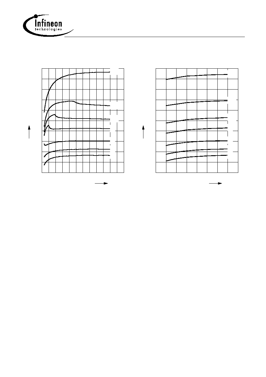
Transition frequency f
T
=
(I
C
)
f = 1 GHz
V
CE
= parameter in V
0
10
20
30
40
mA
60
I
C
4
6
8
10
12
14
16
18
20
GHz
24
f
T
3-4V
2V
1V
Power gain G
ma
, G
ms
, |S
21
|
2
=
(f)
V
CE
= 3 V, I
C
= 20 mA
0
1
2
3
4
GHz
6
f
0
5
10
15
20
25
30
35
40
dB
50
G
Gms
Gma
|S21|≤