 | –≠–ª–µ–∫—Ç—Ä–æ–Ω–Ω—ã–π –∫–æ–º–ø–æ–Ω–µ–Ω—Ç: BFP540 | –°–∫–∞—á–∞—Ç—å:  PDF PDF  ZIP ZIP |
BFP540
Jan-28-2004
1
NPN Silicon RF Transistor
∑
For highest gain low noise amplifier
at 1.8 GHz
∑
Outstanding G
ms
= 21 dB
Noise Figure F = 0.9 dB
∑
Gold metallization for high reliability
∑
SIEGET
45 - Line
VPS05605
4
2
1
3
ESD: Electrostatic discharge sensitive device, observe handling precaution!
Type
Marking
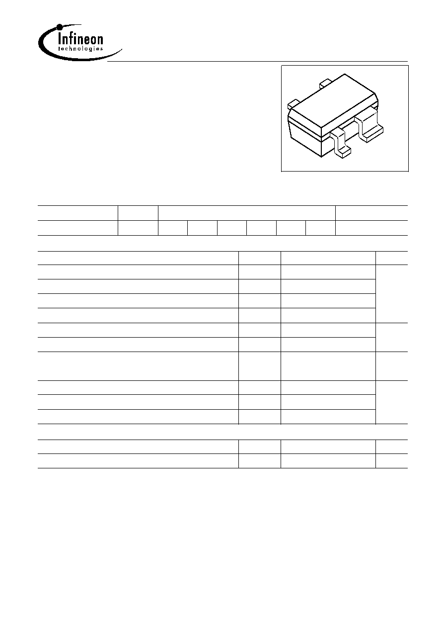
Pin Configuration
Package
BFP540
ATs
1=B
2=E
3=C
4=E
-
-
SOT343
Maximum Ratings
Parameter
Symbol
Value
Unit
Collector-emitter voltage
V
CEO
4.5
V
Collector-emitter voltage
V
CES
14
Collector-base voltage
V
CBO
14
Emitter-base voltage
V
EBO
1
Collector current
I
C
80
mA
Base current
I
B
8
Total power dissipation
1)
T
S
77∞C
P
tot
250
mW
Junction temperature
T
j
150
∞C
Ambient temperature
T
A
-65 ... 150
Storage temperature
T
stg
-65 ... 150
Thermal Resistance
Parameter
Symbol
Value
Unit
Junction - soldering point
2)
R
thJS
290
K/W
1TS is measured on the collector lead at the soldering point to the pcb
2For calculation of R
thJA
please refer to Application Note Thermal Resistance

BFP540
Jan-28-2004
2
Electrical Characteristics at T
A
= 25∞C, unless otherwise specified
Parameter
Symbol
Values
Unit
min.
typ.
max.
DC Characteristics
Collector-emitter breakdown voltage
I
C
= 1 mA, I
B
= 0
V
(BR)CEO
4.5
5
-
V
Collector-emitter cutoff current
V
CE
= 14 V, V
BE
= 0
I
CES
-
-
10
µA
Collector-base cutoff current
V
CB
= 5 V, I
E
= 0
I
CBO
-
-
100
nA
Emitter-base cutoff current
V
EB
= 0.5 V, I
C
= 0
I
EBO
-
-
10
µA
DC current gain
I
C
= 20 mA, V
CE
= 3.5 V
h
FE
50
110
200
-

BFP540
Jan-28-2004
3
Electrical Characteristics at T
A
= 25∞C, unless otherwise specified
Parameter
Symbol
Values
Unit
min.
typ.
max.
AC Characteristics (verified by random sampling)
Transition frequency
I
C
= 50 mA, V
CE
= 4 V, f = 1 GHz
f
T
21
30
-
GHz
Collector-base capacitance
V
CB
= 2 V, f = 1 MHz
C
cb
-
0.14
0.24 pF
Collector emitter capacitance
V
CE
= 2 V, f = 1 MHz
C
ce
-
0.33
-
Emitter-base capacitance
V
EB
= 0.5 V, f = 1 MHz
C
eb
-
0.65
-
Noise figure
I
C
= 5 mA, V
CE
= 2 V, f = 1.8 GHz, Z
S
= Z
Sopt
I
C
= 5 mA, V
CE
= 2 V, f = 3 GHz, Z
S
= Z
Sopt
F
-
-
0.9
1.3
1.4
-
dB
Power gain, maximum stable
1)
I
C
= 20 mA, V
CE
= 2 V, Z
S
= Z
Sopt
,
Z
L
= Z
Lopt
, f = 1.8 GHz
G
ms
-
21.5
-
dB
Power gain, maximum available
1)
I
C
= 20 mA, V
CE
= 2 V, Z
S
= Z
Sopt
,
Z
L
= Z
Lopt
, f = 3 GHz
G
ma
-
16
-
dB
Transducer gain
I
C
= 20 mA, V
CE
= 2 V, Z
S
= Z
L
= 50
,
f = 1.8 GHz
I
C
= 20 mA, V
CE
= 2 V, Z
S
= Z
L
= 50
,
f = 3 GHz
|S
21e
|
2
16
-
18.5
14.5
-
-
dB
Third order intercept point at output
2)
V
CE
= 2 V, I
C
= 20 mA, f = 1.8 GHz,
Z
S
= Z
L
= 50
IP
3
-
24.5
-
dBm
1dB Compression point at output
I
C
= 20 mA, V
CE
= 2 V, Z
S
= Z
L
= 50
,
f = 1.8 GHz
P
-1dB
-
11
-
1
G
ma
= |
S
21e
/
S
12e
| (k-(k≤-1)
1/2
),
G
ms
= |
S
21e
/
S
12e
|
2IP3 value depends on termination of all intermodulation frequency components.
Termination used for this measurement is 50
from 0.1 MHz to 6 GHz
BFP540
Jan-28-2004
4
SPICE Parameter (Gummel-Poon Model, Berkley-SPICE 2G.6 Syntax):
Transitor Chip Data:
IS =
82.84
aA
VAF =
28.383
V
NE =
3.19
-
VAR =
19.705
V
NC =
1.172
-
RBM =
1.3
CJE =
1.8063
fF
TF =
6.76
ps
ITF =
1
mA
VJC =
0.81969
V
TR =
2.324
ns
MJS =
0
-
XTI =
3
-
NF =
1
-
ISE =
11.15
fA
NR =
1
-
ISC =
19.237
aA
IRB =
0.72983
mA
RC =
4
MJE =
0.46576
-
VTF =
0.23794
V
CJC =
234
fF
XCJC =
0.3
-
VJS =
0.75
V
EG =
1.11
eV
TNOM
300
K
BF =
107.5
-
IKF =
0.48731
A
BR =
5.5
-
IKR =
0.02
A
RB =
5.4
RE =
0.31111
-
VJE =
0.8051
V
XTF =
0.4219
-
PTF =
0
deg
MJC =
0.30232
-
CJS =
0
fF
XTB =
0
-
FC =
0.73234
All parameters are ready to use, no scalling is necessary.
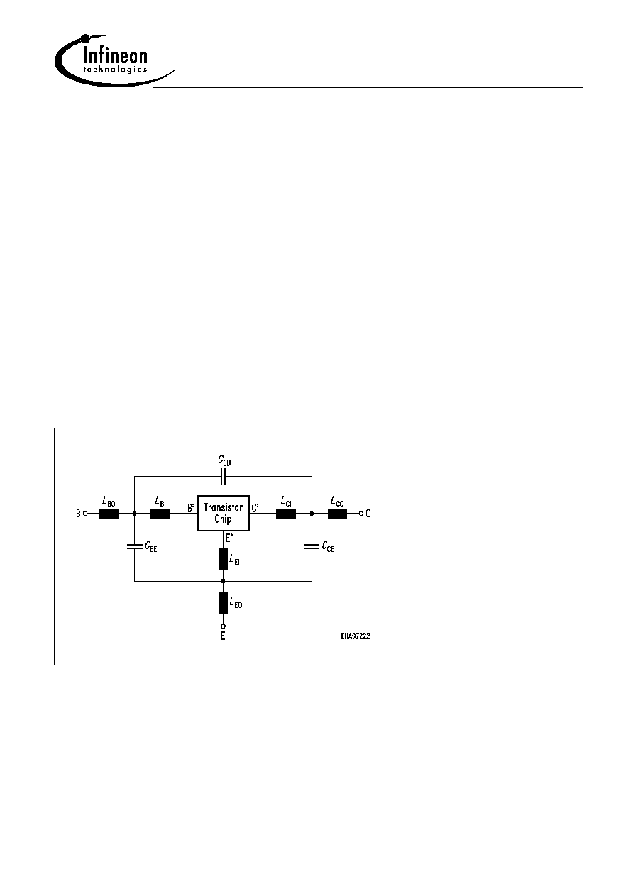
Package Equivalent Circuit:
L
BI
=
0.47
nH
L
BO
=
0.53
nH
L
EI
=
0.23
nH
L
EO
=
0.05
nH
L
CI
=
0.56
pH
L
EO
=
0.58
nH
C
BE
=
136
fF
C
CB
=
6.9
fF
C
CE
=
134
fF
For examples and ready to use parameters
please contact your local Infineon Technologies
distributor or sales office to obtain a Infineon
Technologies CD-ROM or see Internet:
http//www.infineon.com/silicondiscretes
Valid up to 6GHz
For non-linear simulation:
∑
Use transistor chip parameters in Berkeley SPICE 2G.6 syntax for all simulators.
∑
Simulation of the package is not necessary for frequencies < 100MHz.
For higher frequencies please add the wiring of the package equivalent circuit
around the non-linear transistor.
BFP540
Jan-28-2004
5
Total power dissipation P
tot
=
(
T
S
)
0
20
40
60
80
100
120 ∞C
150
T
S
0
50
100
150
200
mW
300
P
tot
Permissible Pulse Load R
thJS
=
(
t
p
)
10
-7
10
-6
10
-5
10
-4
10
-3
10
-2
10
0
s
t
p
1
10
2
10
3
10
K/W
R
thJS
0.5
0.2
0.1
0.05
0.02
0.01
0.005
D = 0
Permissible Pulse Load
P
totmax
/
P
totDC
=
(
t
p
)
10
-7
10
-6
10
-5
10
-4
10
-3
10
-2
10
0
s
t
p
0
10
1
10
P
totmax
/
P
totDC
D = 0
0.005
0.01
0.02
0.05
0.1
0.2
0.5
Collector-base capacitance C
cb
=
(
V
CB
)
f = 1MHz
0
0.5
1
1.5
2
2.5
3
V
4
V
CB
0
0.05
0.1
pF
0.2
C
cb
BFP540
Jan-28-2004
6
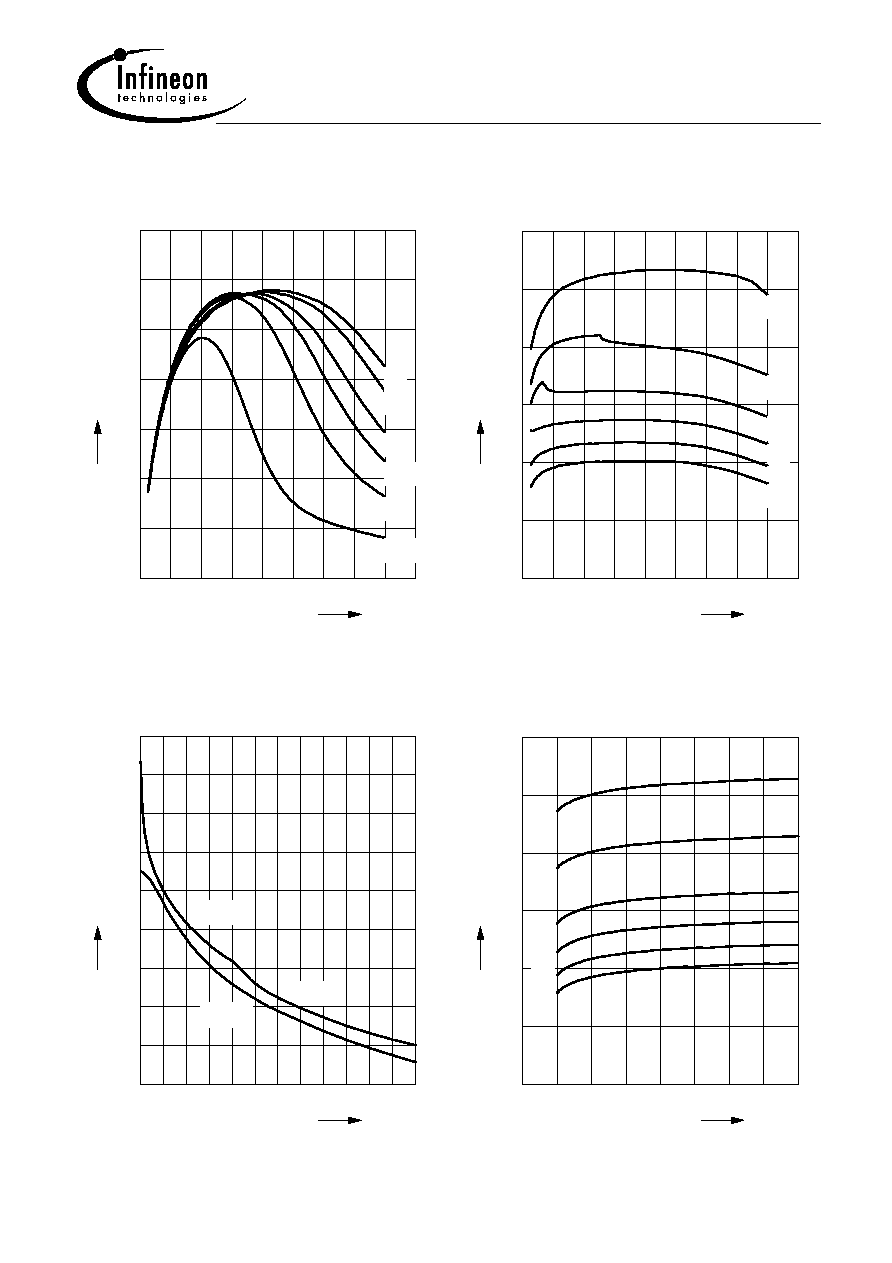
Transition frequency f
T
=
(
I
C
)
f = 1GHz
V
CE
= Parameter in V
0
10
20
30
40
50
60
70 mA
90
I
C
0
5
10
15
20
25
GHz
35
f
T
0.5
1
1.5
2
3
4
Power gain G
ma
,
G
ms
=
(
I
C
)
V
CE
= 2V
f = Parameter in GHz
0
10
20
30
40
50
60
70 mA
90
I
C
0
5
10
15
20
dB
30
G
1
2
3
4
5
6
Power Gain G
ma
,
G
ms
=
(
f),
|
S
21
|≤ =
f (f)
V
CE
= 2V,
I
C
= 20mA
0
1
2
3
4
GHz
6
G
5
10
15
20
25
30
35
40
dB
50
I
C
|S21|≤
Gms
Gma
Power gain G
ma
,
G
ms
=
(
V
CE
)
I
C
= 20mA
f = Parameter in GHz
0
0.5
1
1.5
2
2.5
3
V
4
V
CE
0
5
10
15
20
dB
30
G
1
2
3
4
5
6
BFP540
Jan-28-2004
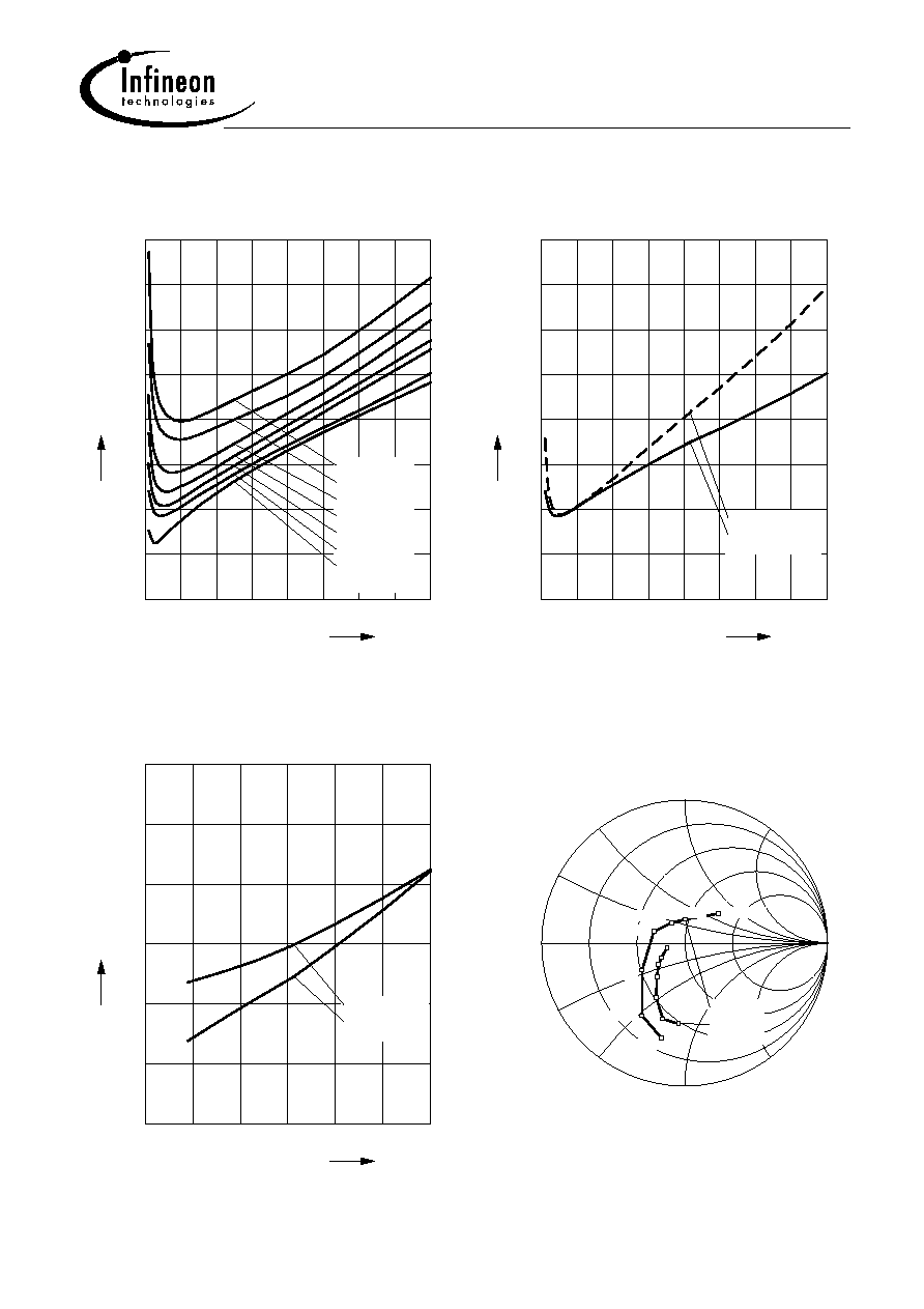
7
Noise figure F =
(
I
C
)
V
CE
= 2V,
Z
S
=
Z
Sopt
0
10
20
30
40
50
60
mA
80
I
C
0
0.5
1
1.5
2
2.5
3
dB
4
F
f = 6GHz
f = 5GHz
f = 4GHz
f = 3GHz
f = 2.4GHz
f = 1.8GHz
f = 0.9GHz
Noise figure F =
(
I
C
)
V
CE
= 2V,
f = 1.8GHz
0
10
20
30
40
50
60
mA
80
I
C
0
0.5
1
1.5
2
2.5
3
dB
4
F
ZS = 50Ohm
ZS = Zsopt
Noise figure F =
(
f)
V
CE
= 2V,
Z
S
=
Z
Sopt
0
1
2
3
4
GHz
6
f
0
0.5
1
1.5
2
dB
3
F
IC = 20mA
IC = 5mA
Source impedance for min.
noise figure vs. frequency
V
CE
= 2V,
I
C
= 5mA / 20mA
100
+j10
-j10
50
+j25
-j25
25
+j50
-j50
10
+j100
-j100
0
0.9GHz
1.8GHz
2.4GHz
3GHz
4GHz
5GHz
6GHz
5mA
20mA