 | –≠–ª–µ–∫—Ç—Ä–æ–Ω–Ω—ã–π –∫–æ–º–ø–æ–Ω–µ–Ω—Ç: BFP650 | –°–∫–∞—á–∞—Ç—å:  PDF PDF  ZIP ZIP |
BFP650
Jan-08-2004
1
NPN Silicon Germanium RF Transistor
Preliminary data
∑
For high power amplifiers
∑
Ideal for low phase noise oscilators
∑
Maxim. available Gain G
ma
= 21 dB at 1.8 GHz
Noise figure F = 0.9 dB at 1.8 GHz
∑
Gold metallization for high reliability
∑
70 GHz f
T
- Silicon Germanium technology
VPS05605
4
2
1
3
ESD
: Electrostatic discharge sensitive device, observe handling precaution!
Type
Marking
Pin Configuration
Package
BFP650
R5s
1=B
2=E
3=C
4=E
-
-
SOT343
Maximum Ratings
Parameter
Symbol
Value
Unit
Collector-emitter voltage
V
CEO
4
V
Collector-emitter voltage
V
CES
13
Collector-base voltage
V
CBO
13
Emitter-base voltage
V
EBO
1.2
Collector current
I
C
150
mA
Base current
I
B
10
Total power dissipation
1)
T
S
75∞C
P
tot
500
mW
Junction temperature
T
j
150
∞C
Ambient temperature
T
A
-65 ... 150
Storage temperature
T
stg
-65 ... 150
Thermal Resistance
Parameter
Symbol
Value
Unit
Junction - soldering point
2)
R
thJS
140
K/W
1TS is measured on the collector lead at the soldering point to the pcb
2For calculation of R
thJA
please refer to Application Note Thermal Resistance

BFP650
Jan-08-2004
2
Electrical Characteristics at T
A
= 25∞C, unless otherwise specified
Parameter
Symbol
Values
Unit
min.
typ.
max.
DC Characteristics
Collector-emitter breakdown voltage
I
C
= 3 mA, I
B
= 0
V
(BR)CEO
4
4.5
-
V
Collector-emitter cutoff current
V
CE
= 13 V, V
BE
= 0
I
CES
-
-
100
µA
Collector-base cutoff current
V
CB
= 5 V, I
E
= 0
I
CBO
-
-
100
nA
Emitter-base cutoff current
V
EB
= 0.5 V, I
C
= 0
I
EBO
-
-
10
µA
DC current gain
I
C
= 80 mA, V
CE
= 3 V
h
FE
100
180
320
-

BFP650
Jan-08-2004
3
Electrical Characteristics at T
A
= 25∞C, unless otherwise specified
Parameter
Symbol
Values
Unit
min.
typ.
max.
AC Characteristics (verified by random sampling)
Transition frequency
I
C
= 80 mA, V
CE
= 3 V, f = 1 GHz
f
T
-
37
-
GHz
Collector-base capacitance
V
CB
= 3 V, f = 1 MHz
C
cb
-
0.26
-
pF
Collector emitter capacitance
V
CE
= 3 V, f = 1 MHz
C
ce
-
0.45
-
Emitter-base capacitance
V
EB
= 0.5 V, f = 1 MHz
C
eb
-
1.1
-
Noise figure
I
C
= 10 mA, V
CE
= 3 V, f = 1.8 GHz, Z
S
= Z
Sopt
I
C
= 10 mA, V
CE
= 3 V, f = 6 GHz, Z
S
= Z
Sopt
F
-
-
0.8
1.9
-
-
dB
Power gain, maximum available
1)
I
C
= 80 mA, V
CE
= 3 V, Z
S
= Z
Sopt
,
Z
L
= Z
Lopt
, f = 1.8 GHz
I
C
= 80 mA, V
CE
= 3 V, Z
S
= Z
Sopt
,
Z
L
= Z
Lopt
, f = 6 GHz
G
ma
-
-
21
10.5
-
-
Transducer gain
I
C
= 80 mA, V
CE
= 3 V, Z
S
= Z
L
= 50
,
f = 1.8 GHz
I
C
= 80 mA, V
CE
= 3 V, Z
S
= Z
L
= 50
,
f = 6 GHz
|S
21e
|
2
-
-
17
6
-
-
dB
Third order intercept point at output
2)
V
CE
= 3 V, I
C
= 80 mA, f = 1.8 GHz,
Z
S
= Z
L
= 50
IP
3
-
29.5
-
dBm
1dB Compression point at output
I
C
= 80 mA, V
CE
= 3 V, Z
S
= Z
L
= 50
,
f = 1.8 GHz
P
-1dB
-
18
-
1
G
ma
= |
S
21e
/
S
12e
| (k-(k≤-1)
1/2
)
2IP3 value depends on termination of all intermodulation frequency components.
Termination used for this measurement is 50
from 0.1 MHz to 6 GHz
BFP650
Jan-08-2004
4
SPICE Parameter (Gummel-Poon Model, Berkley-SPICE 2G.6 Syntax):
Transitor Chip Data:
IS =
0.61
fA
VAF =
1000
V
NE =
2
-
VAR =
2
V
NC =
1.8
-
RBM =
0.895
CJE =
682.5
fF
TF =
1.9
ps
ITF =
1.25
A
VJC =
0.6
V
TR =
0.2
ns
MJS =
0.27
-
XTI =
3
-
AF =
2
-
TITF1
-0.0065
-
NF =
1.025
-
ISE =
62
fA
NR =
1
-
ISC =
700
fA
IRB =
4.548
mA
RC =
1.006
MJE =
0.3
-
VTF =
1.5
V
CJC =
204.6
fF
XCJC =
1
-
VJS =
0.6
V
EG =
1.078
eV
TNOM
298
K
BF =
450
-
IKF =
0.47
A
BR =
42
-
IKR =
18
mA
RB =
1.036
RE =
0.2
-
VJE =
0.8
V
XTF =
10
-
PTF =
0
deg
MJC =
0.5
-
CJS =
294.9
fF
XTB =
-1.42
-
FC =
0.8
KF =
2.441E-11
TITF2
1.0E-5
All parameters are ready to use, no scalling is necessary. Extracted on behalf of Infineon Technologies AG by:
Institut f¸r Mobil- und Satellitentechnik (IMST)
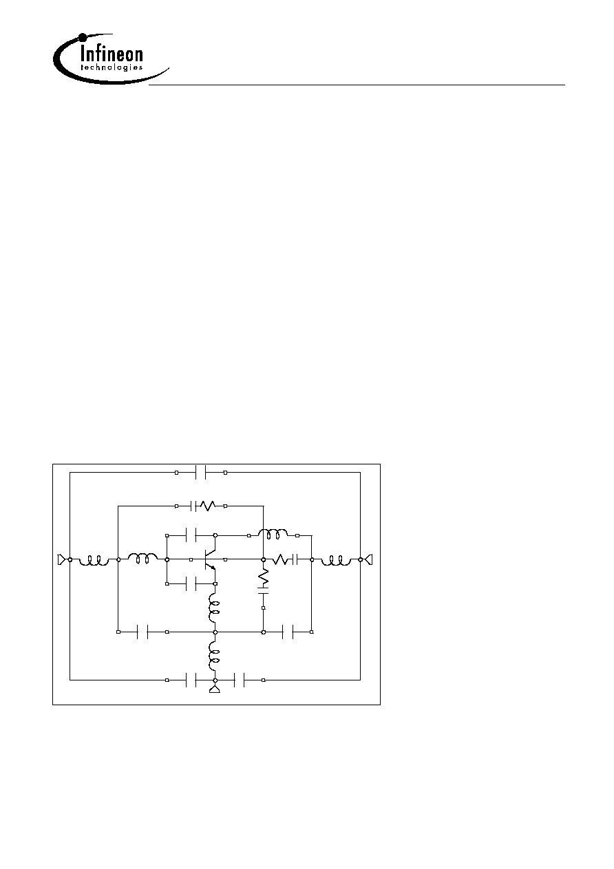
Package Equivalent Circuit:
B
C
E
C C E O
C B E O
C C E I
C B E I
C B E C
C B C C
S
C
B
E
B F P 6 5 0 _ C h i p
L B C
L C C
L E C
R C B S
R C C S
R C E S
L B B
L C B
L E B
I t f = 1 2 5 0 * ( 1 - 6 . 5 e - 3 * ( T - 2 5 ) + 1 . 0 e - 5 * ( T - 2 5 ) ^ 2 )
T = 2 5 ∞ C
C B C O
LBC =
50
pH
LCC =
50
pH
LEC =
4
pH
LBB =
554.6
pH
LCB =
606.9
pH
LEB =
138.7
pH
CBEC = 327.6
fF
CBCC = 171.4
fF
CES =
490
fF
CBS =
120
fF
CCS =
135
fF
CBCO = 7.5
fF
CCEO = 112.6
fF
CBEO = 121.5
fF
CCEI =
5.7
fF
CBEI =
6.9
RBS =
710
RCS =
710
RES =
140
For examples and ready to use parameters
please contact your local Infineon Technologies
distributor or sales office to obtain a Infineon
Technologies CD-ROM or see Internet:
http//www.infineon.com/silicondiscretes
Valid up to 6GHz
BFP650
Jan-08-2004
5
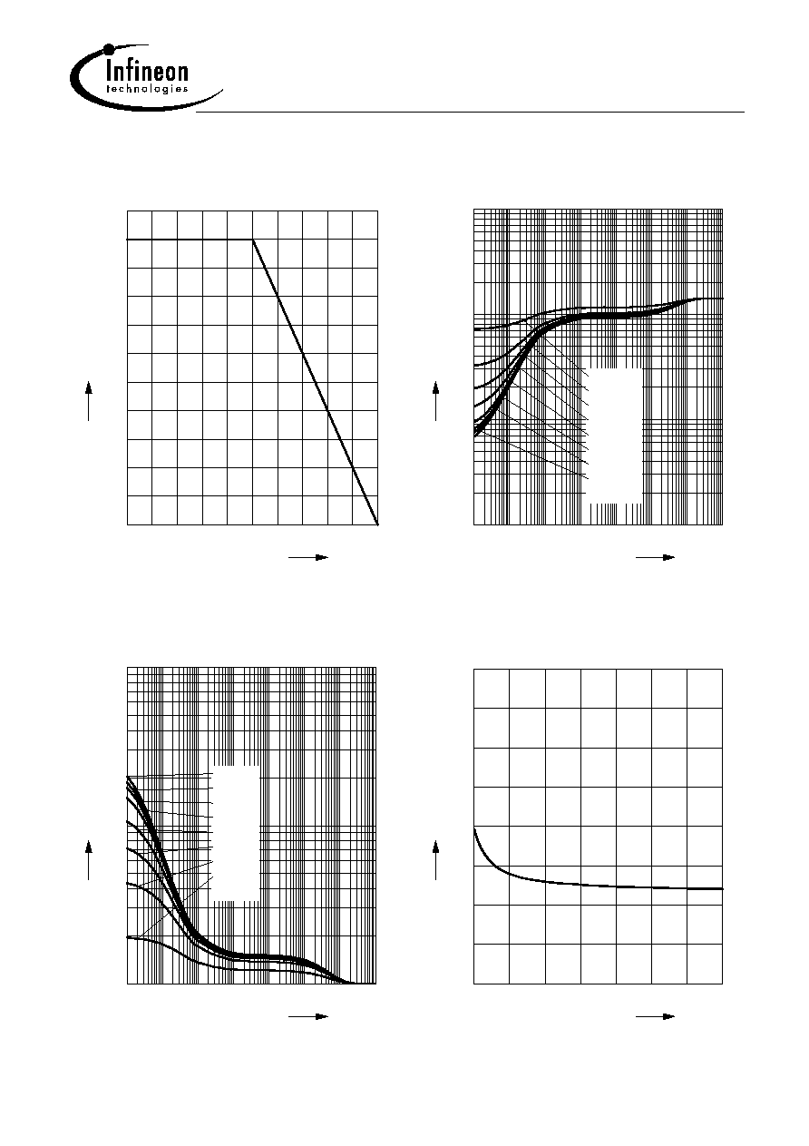
Total power dissipation P
tot
=
(
T
S
)
0
15
30
45
60
75
90 105 120 ∞C
150
T
S
0
50
100
150
200
250
300
350
400
450
mW
550
P
tot
Permissible Pulse Load R
thJS
=
(
t
p
)
10
-7
10
-6
10
-5
10
-4
10
-3
10
-2
10
0
∞C
t
p
0
10
1
10
2
10
3
10
K/W
R
thJS
D = 0.5
0.2
0.1
0.05
0.02
0.01
0.005
0
Permissible Pulse Load
P
totmax
/
P
totDC
=
(
t
p
)
10
-7
10
-6
10
-5
10
-4
10
-3
10
-2
10
0
s
t
p
0
10
1
10
2
10
-
P
totmax
/
P
totDC
D = 0
0.005
0.01
0.02
0.05
0.1
0.2
0.5
Collector-base capacitance C
cb
=
(
V
CB
)
f = 1MHz
0
2
4
6
8
10
V
14
V
CB
0
0.1
0.2
0.3
0.4
0.5
0.6
pF
0.8
C
CB
BFP650
Jan-08-2004
6
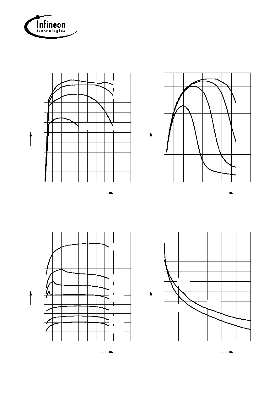
Third order Intercept Point IP
3
=
(
I
C
)
(Output, Z
S
=Z
L
=50
)
V
CE
= parameter,
f = 1.8 GHz
0
15
30
45
60
75
90 105 120 mA 150
I
C
0
3
6
9
12
15
18
21
24
27
dBm
33
I
P3
1V
2V
3V
4V
Transition frequency f
T
=
(
I
C
)
f = 1GHz
V
CE
= parameter
0
20
40
60
80
100 120 140 mA
180
I
C
0
5
10
15
20
25
30
GHz
40
f
T
3V
2V
1V
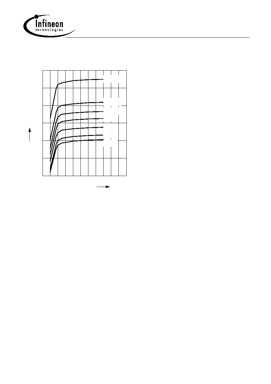
0.5V
Power gain G
ma
,
G
ms
=
(
I
C
)
V
CE
= 3V
f = parameter
0
20
40
60
80 100 120 140 160 mA 200
I
C
6
8
10
12
14
16
18
20
22
24
26
dB
30
G
0.9GHz
1.8GHz
2.4GHz
3GHz
4GHz
5GHz
6GHz
Power Gain G
ma
,
G
ms
=
(
f),
|
S
21
|≤ =
f (f)
V
CE
= 3V,
I
C
= 80mA
0
1
2
3
4
GHz
6
f
0
5
10
15
20
25
30
35
40
45
dB
55
G
Gms
Gma
S21≤
BFP650
Jan-08-2004
7
Power gain G
ma
,
G
ms
=
(
V
CE
)
I
C
= 80mA
f = parameter
0
1
2
3
4
V
5.5
V
CE
0
5
10
15
20
dB
30
G
0.9GHz
1.8GHz
2.4GHz
3GHz
4GHz
5GHz
6GHz