BFR181W
Jun-27-2001
1
NPN Silicon RF Transistor
For low noise, high-gain broadband amplifiers at
collector currents from 0.5 mA to 12 mA
f
T
= 8 GHz
F = 1.45 dB at 900 MHz
1
3
VSO05561
2
ESD: Electrostatic discharge sensitive device, observe handling precaution!
Type
Marking
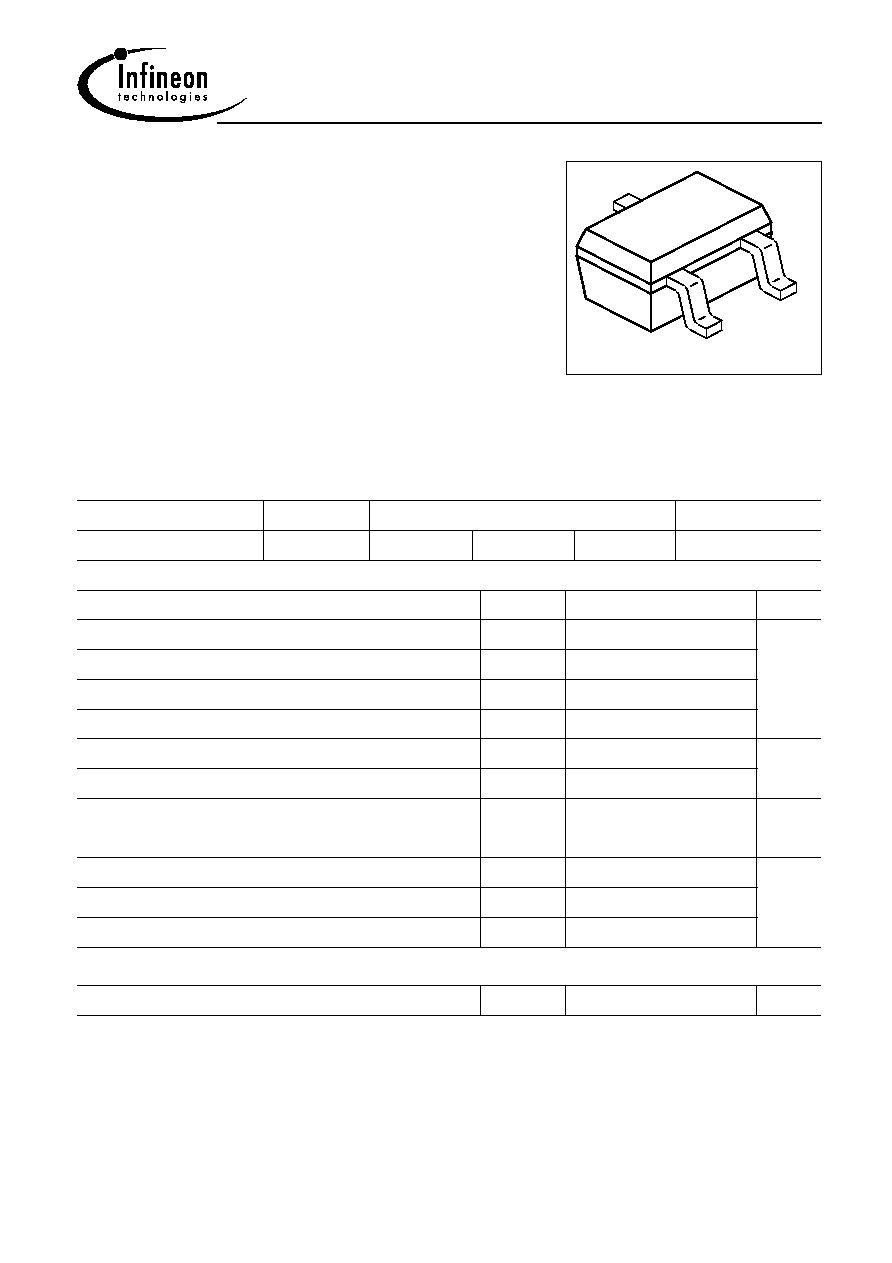
Pin Configuration
Package
BFR181W
RFs
1 = B
2 = E
3 = C
SOT323
Maximum Ratings
Parameter
Symbol
Value
Unit
Collector-emitter voltage
V
CEO
12
V
Collector-emitter voltage
V
CES
20
Collector-base voltage
V
CBO
20
Emitter-base voltage
V
EBO
2
Collector current
I
C
20
mA
Base current
I
B
2
Total power dissipation
T
S
90 �C
1)
P
tot
175
mW
Junction temperature
T
j
150
�C
Ambient temperature
T
A
-65 ... 150
Storage temperature
T
stg
-65 ... 150
Thermal Resistance
Junction - soldering point
2)
R
thJS
345
K/W
1T
S
is measured on the collector lead at the soldering point to the pcb
2For calculation of R
thJA
please refer to Application Note Thermal Resistance

BFR181W
Jun-27-2001
2
Electrical Characteristics at T
A
= 25�C, unless otherwise specified.
Parameter
Symbol
Values
Unit
min.
typ.
max.
DC characteristics
Collector-emitter breakdown voltage
I
C
= 1 mA, I
B
= 0
V
(BR)CEO
12
-
-
V
Collector-emitter cutoff current
V
CE
= 20 V, V
BE
= 0
I
CES
-
-
100
�A
Collector-base cutoff current
V
CB
= 10 V, I
E
= 0
I
CBO
-
-
100
nA
Emitter-base cutoff current
V
EB
= 1 V, I
C
= 0
I
EBO
-
-
1
�A
DC current gain
I
C
= 5 mA, V
CE
= 8 V
h
FE
50
100
200
-

BFR181W
Jun-27-2001
3
Electrical Characteristics at T
A
= 25�C, unless otherwise specified.
Parameter
Symbol
Values
Unit
min.
typ.
max.
AC characteristics
(verified by random sampling)
Transition frequency
I
C
= 10 mA, V
CE
= 8 V, f = 500 MHz
f
T
6
8
-
GHz
Collector-base capacitance
V
CB
= 10 V, f = 1 MHz
C
cb
-
0.32
0.5
pF
Collector-emitter capacitance
V
CE
= 10 V, f = 1 MHz
C
ce
-
0.22
-
Emitter-base capacitance
V
EB
= 0.5 V, f = 1 MHz
C
eb
-
0.3
-
Noise figure
I
C
= 2 mA, V
CE
= 8 V, Z
S
= Z
Sopt
,
f
= 900 MHz
f
= 1.8 GHz
F
-
-
1.45
1.8
-
-
dB
Power gain, maximum stable
1)
I
C
= 5 mA, V
CE
= 8 V, Z
S
= Z
Sopt
, Z
L
= Z
Lopt
,
f
= 900 MHz
G
ms
-
18.5
-
Power gain, maximum available
2)
I
C
= 5 mA, V
CE
= 8 V, Z
S
= Z
Sopt
, Z
L
= Z
Lopt
,
f
= 1.8 GHz
G
ma
-
13
-
Transducer gain
I
C
= 5 mA, V
CE
= 8 V, Z
S
= Z
L
= 50
,
f
= 900 MHz
f
= 1.8 GHz
|S
21e
|
2
-
-
15
9.5
-
-
1
G
ms
= |S
21
/ S
12
|
2
G
ma
= |S
21
/ S
12
| (k-(k
2
-1)
1/2
)
BFR181W
Jun-27-2001
4
SPICE Parameters (Gummel-Poon Model, Berkley-SPICE 2G.6 Syntax) :
Transistor Chip Data
IS =
0.0010519 fA
VAF =
22.403
V
NE =
1.7631
-
VAR =
5.1127
V
NC =
1.6528
-
RBM =
6.6315
CJE =
1.8168
fF
TF =
17.028
ps
ITF =
1.0549
mA
VJC =
1.1633
V
TR =
2.7449
ns
MJS =
0
-
XTI =
3
-
BF =
96.461
-
IKF =
0.12146
A
BR =
16.504
-
IKR =
0.24951
A
RB =
9.9037
RE =
2.1372
VJE =
0.73155
V
XTF =
0.33814
-
PTF =
0
deg
MJC =
0.30013
-
CJS =
0
fF
XTB =
0
-
FC =
0.99768
-
NF =
0.90617
-
ISE =
12.603
fA
NR =
0.87757
-
ISC =
0.01195
fA
IRB =
0.69278
mA
RC =
2.2171
MJE =
0.43619
-
VTF =
0.12571
V
CJC =
319.69
fF
XCJC =
0.082903
-
VJS =
0.75
V
EG =
1.11
eV
TNOM
300
K
All parameters are ready to use, no scalling is necessary.
Extracted on behalf of Infineon Technologies AG by:
Institut f�r Mobil-und Satellitentechnik (IMST)
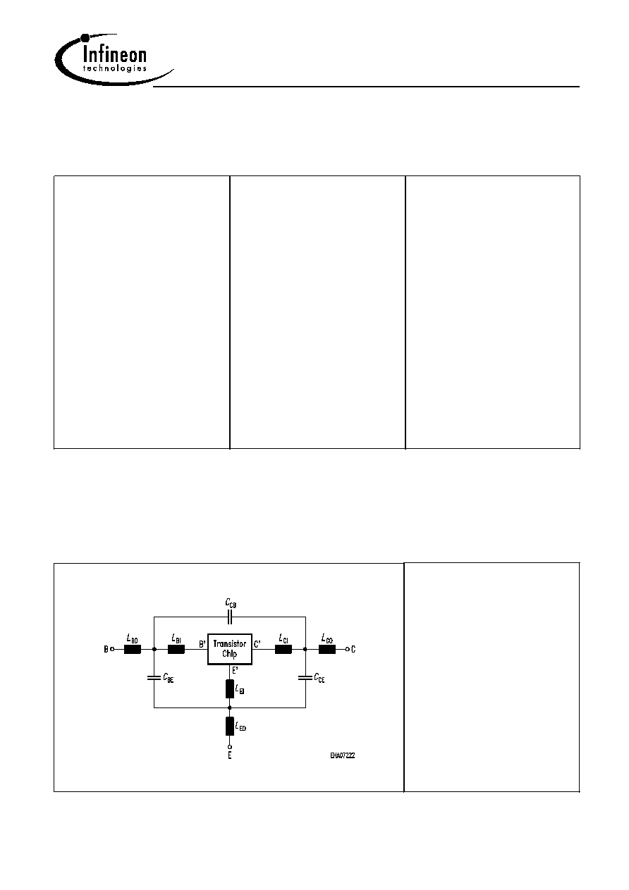
Package Equivalent Circuit:
L
BI
=
0.57
nH
L
BO
=
0.4
nH
L
EI
=
0.43
nH
L
EO
=
0.5
nH
L
CI
=
0
nH
L
CO
=
-
nH
C
BE
=
61
fF
C
CB
=
101
fF
C
CE
=
175
fF
Valid up to 6GHz
For examples and ready to use parameters please contact your local Infineon Technologies distributor or sales
office to obtain a Infineon Technologies CD-ROM or see Internet: http://www.infineon.com/products/discrete/index.htm
BFR181W
Jun-27-2001
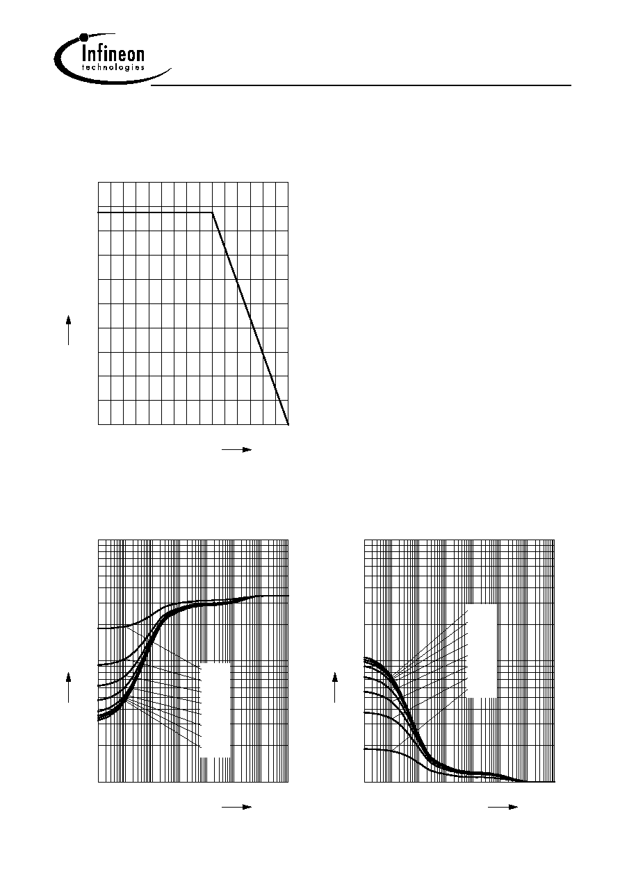
5
Total power dissipation P
tot
= f (T
S
)
0
20
40
60
80
100
120 �C
150
T
S
0
20
40
60
80
100
120
140
160
mW
200
P
tot
Permissible Pulse Load R
thJS
= f (t
p
)
10
-7
10
-6
10
-5
10
-4
10
-3
10
-2
10
0
s
t
p
1
10
2
10
3
10
K/W
R
thJS
0.5
0.2
0.1
0.05
0.02
0.01
0.005
D = 0
Permissible Pulse Load
P
totmax
/P
totDC
= f (t
p
)
10
-7
10
-6
10
-5
10
-4
10
-3
10
-2
10
0
s
t
p
0
10
1
10
2
10
-
P
tot
m
ax
/ P
totDC
D = 0
0.005
0.01
0.02
0.05
0.1
0.2
0.5
BFR181W
Jun-27-2001
6
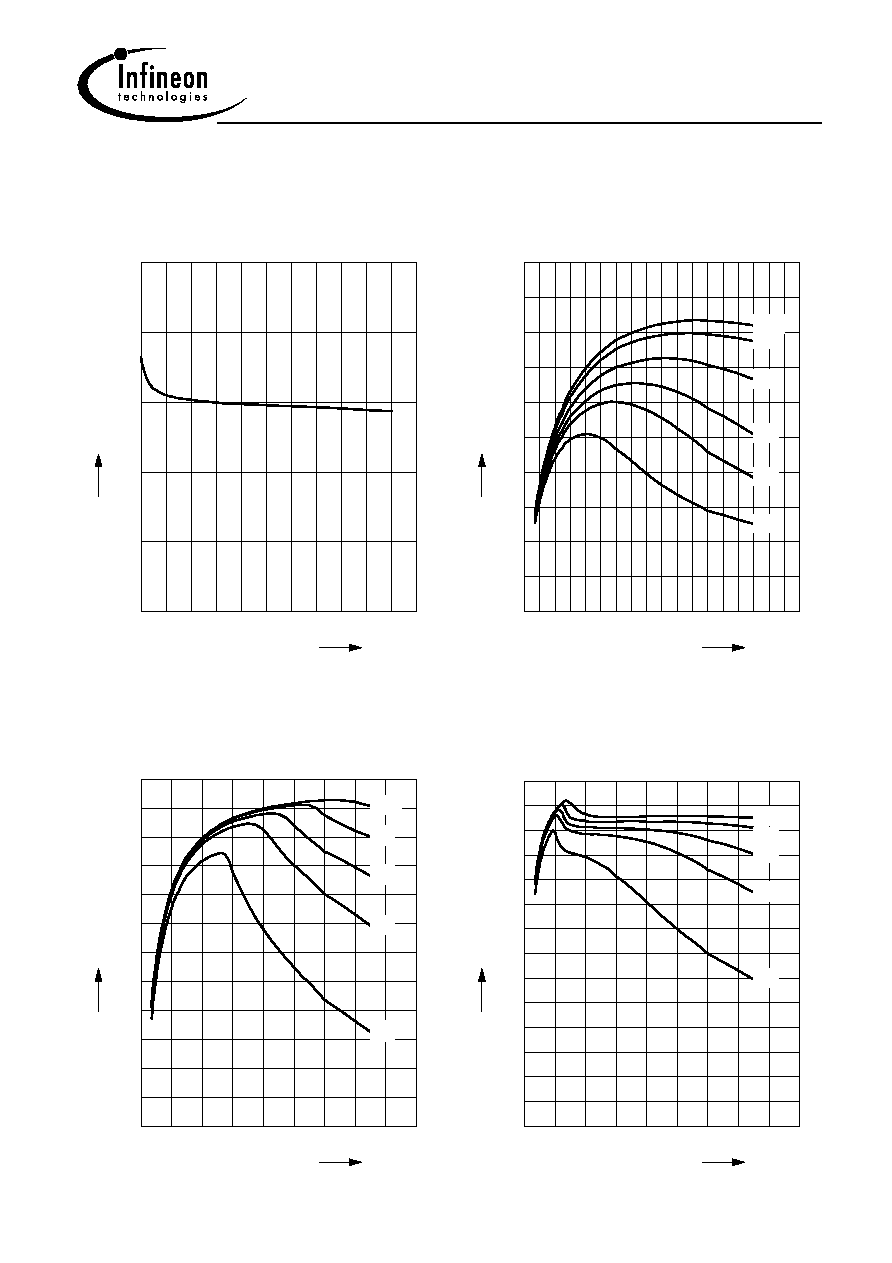
Collector-base capacitance C
cb
= f (V
CB
)
f = 1MHz
0
4
8
12
16
V
22
V
CB
0.0
0.1
0.2
0.3
pF
0.5
C
cb
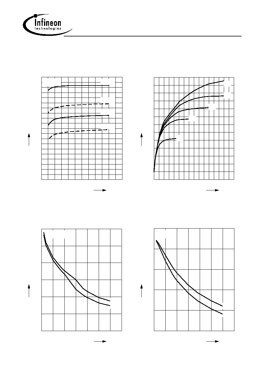
Transition frequency f
T
= f (I
C
)
V
CE
= Parameter
0
2
4
6
8
10
12
14 mA
18
f
T
0
1
2
3
4
5
6
7
8
GHz
10
f
T
10V
8V
5V
3V
2V
1V
Power Gain G
ma
, G
ms
= f(I
C
)
f = 0.9GHz
V
CE
= Parameter
0
2
4
6
8
10
12
14 mA
18
I
C
8
9
10
11
12
13
14
15
16
17
18
dB
20
G
10V
3V
2V
1V
5V
Power Gain G
ma
, G
ms
= f(I
C
)
f = 1.8GHz
V
CE
= Parameter
0
2
4
6
8
10
12
14 mA
18
I
C
0
1
2
3
4
5
6
7
8
9
10
11
12
dB
14
G
10V
3V
2V
1V
5V
BFR181W
Jun-27-2001
7
Intermodulation Intercept Point IP
3
=f(I
C
)
(3rd order, Output,
Z
S
=Z
L
=50
)
V
CE
= Parameter, f = 900MHz
1
3
5
7
9
11
13
mA
17
I
C
-4
-2
0
2
4
6
8
10
12
14
16
18
dBm
22
IP
3
8V
5V
3V
2V
1V
Power Gain G
ma
, G
ms
= f(V
CE
):_____
|S
21
|
2
= f(V
CE
):---------
f = Parameter
0
2
4
6
8
V
12
V
CE
0
2
4
6
8
10
12
14
16
dB
20
G
0.9GHz
1.8GHz
0.9GHz
1.8GHz
I
C
=5mA
Power Gain |S
21
|
2
= f(f)
V
CE
=
Parameter
0.0
0.5
1.0
1.5
2.0
2.5
GHz
3.5
f
0
5
10
15
dB
25
S
21
10V
1V
I
C
=5mA
Power Gain G
ma
, G
ms
= f(f)
V
CE
= Parameter
0.0
0.5
1.0
1.5
2.0
2.5
GHz
3.5
f
0
5
10
15
20
dB
30
G
10V
1V
I
C
=5mA