BFR193W
Aug-09-2001
1
NPN Silicon RF Transistor
For low noise, high-gain amplifiers up to 2 GHz
For linear broadband amplifiers
f
T
= 8 GHz
F = 1.3 dB at 900 MHz
1
3
VSO05561
2
ESD: Electrostatic discharge sensitive device, observe handling precaution!
Type
Marking
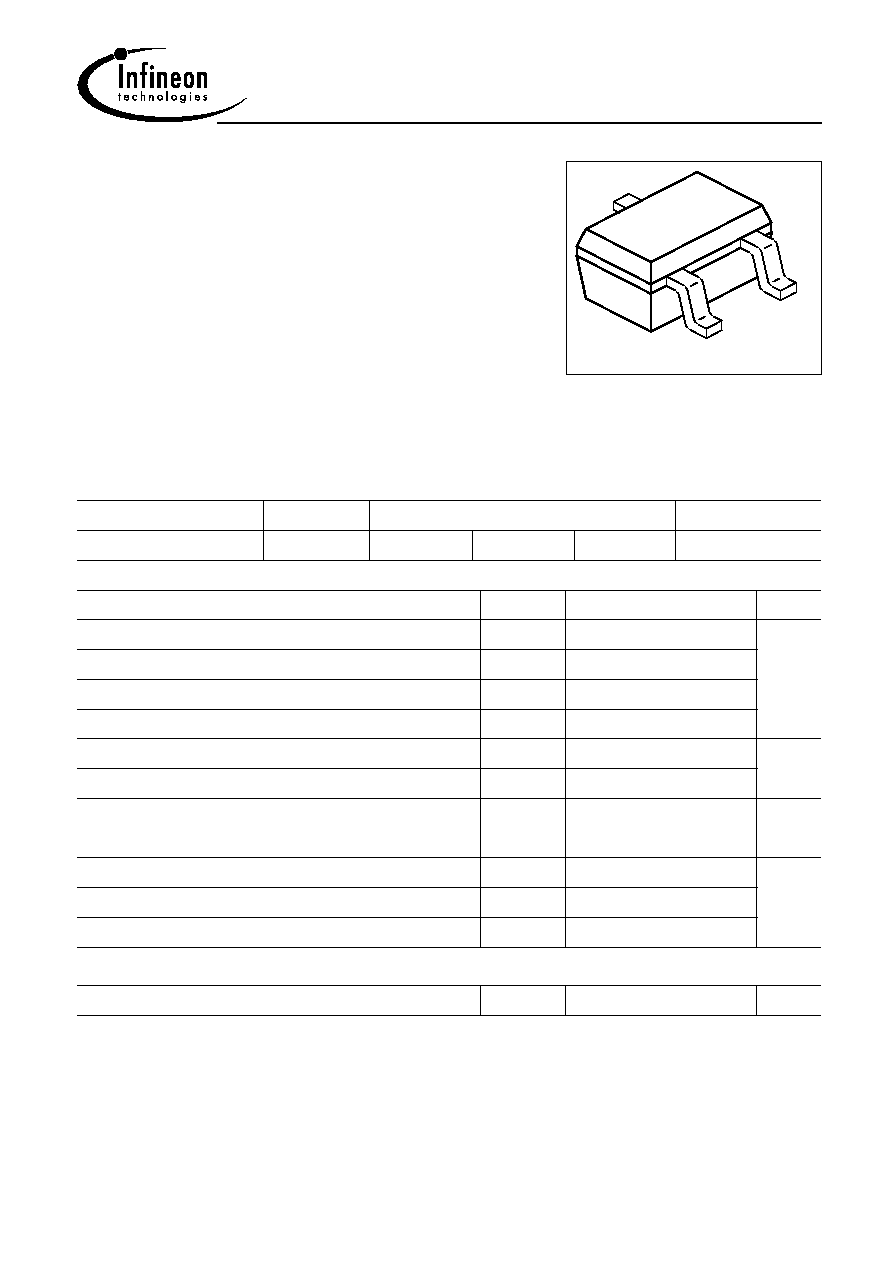
Pin Configuration
Package
BFR193W
RCs
1 = B
2 = E
3 = C
SOT323
Maximum Ratings
Parameter
Symbol
Value
Unit
Collector-emitter voltage
V
CEO
12
V
Collector-emitter voltage
V
CES
20
Collector-base voltage
V
CBO
20
Emitter-base voltage
V
EBO
2
Collector current
I
C
80
mA
Base current
I
B
10
Total power dissipation
T
S
63 �C
1)
P
tot
580
mW
Junction temperature
T
j
150
�C
Ambient temperature
T
A
-65 ... 150
Storage temperature
T
stg
-65 ... 150
Thermal Resistance
Junction - soldering point
2)
R
thJS
150
K/W
1T
S
is measured on the collector lead at the soldering point to the pcb
2For calculation of R
thJA
please refer to Application Note Thermal Resistance

BFR193W
Aug-09-2001
2
Electrical Characteristics at T
A
= 25�C, unless otherwise specified.
Parameter
Symbol
Values
Unit
min.
typ.
max.
DC characteristics
Collector-emitter breakdown voltage
I
C
= 1 mA, I
B
= 0
V
(BR)CEO
12
-
-
V
Collector-emitter cutoff current
V
CE
= 20 V, V
BE
= 0
I
CES
-
-
100
�A
Collector-base cutoff current
V
CB
= 10 V, I
E
= 0
I
CBO
-
-
100
nA
Emitter-base cutoff current
V
EB
= 1 V, I
C
= 0
I
EBO
-
-
1
�A
DC current gain
I
C
= 30 mA, V
CE
= 8 V
h
FE
50
100
200
-

BFR193W
Aug-09-2001
3
Electrical Characteristics at T
A
= 25�C, unless otherwise specified.
Parameter
Symbol
Values
Unit
min.
typ.
max.
AC characteristics
(verified by random sampling)
Transition frequency
I
C
= 50 mA, V
CE
= 8 V, f = 500 MHz
f
T
6
8
-
GHz
Collector-base capacitance
V
CB
= 10 V, f = 1 MHz
C
cb
-
0.74
1
pF
Collector-emitter capacitance
V
CE
= 10 V, f = 1 MHz
C
ce
-
0.28
-
Emitter-base capacitance
V
EB
= 0.5 V, f = 1 MHz
C
eb
-
1.8
-
Noise figure
I
C
= 10 mA, V
CE
= 8 V, Z
S
= Z
Sopt
,
f
= 900 MHz
f
= 1.8 GHz
F
-
-
1.3
2.1
-
-
dB
Power gain, maximum available
1)
I
C
= 30 mA, V
CE
= 8 V, Z
S
= Z
Sopt
, Z
L
= Z
Lopt
,
f
= 900 MHz
f
= 1.8 GHz
G
ma
-
-
15.5
10
-
-
Transducer gain
I
C
= 30 mA, V
CE
= 8 V, Z
S
= Z
L
= 50
,
f
= 900 MHz
f
= 1.8 GHz
|S
21e
|
2
-
-
13.5
7.5
-
-
1
G
ma
= |S
21
/ S
12
| (k-(k
2
-1)
1/2
)
BFR193W
Aug-09-2001
4
SPICE Parameters (Gummel-Poon Model, Berkley-SPICE 2G.6 Syntax) :
Transistor Chip Data
IS =
0.2738
fA
VAF =
24
V
NE =
1.935
-
VAR =
3.8742
V
NC =
0.94371
-
RBM =
1
CJE =
1.1824
fF
TF =
18.828
ps
ITF =
0.96893
mA
VJC =
1.1828
V
TR =
1.0037
ns
MJS =
0
-
XTI =
3
-
BF =
125
-
IKF =
0.26949
A
BR =
14.267
-
IKR =
0.037925
A
RB =
1.8368
RE =
0.76534
VJE =
0.70276
V
XTF =
0.69477
-
PTF =
0
deg
MJC =
0.30002
-
CJS =
0
fF
XTB =
0
-
FC =
0.72063
-
NF =
0.95341
-
ISE =
10.627
fA
NR =
1.4289
-
ISC =
0.037409
fA
IRB =
0.91763
mA
RC =
0.11938
MJE =
0.48654
-
VTF =
0.8
V
CJC =
935.03
fF
XCJC =
0.053563
-
VJS =
0.75
V
EG =
1.1
eV
TNOM
300
K
All parameters are ready to use, no scalling is necessary.
Extracted on behalf of Infineon Technologies AG by:
Institut f�r Mobil-und Satellitentechnik (IMST)
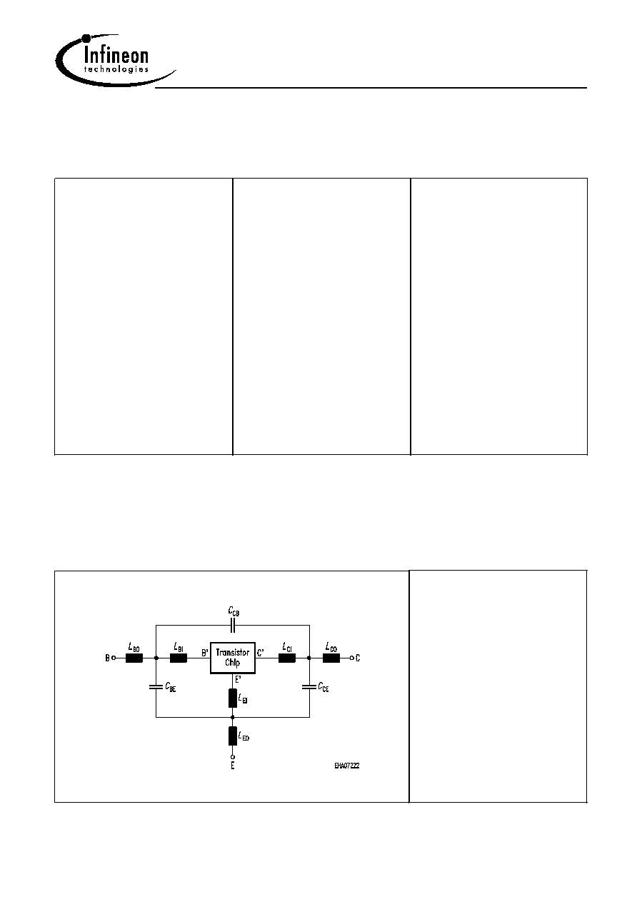
Package Equivalent Circuit:
L
BI
=
0.57
nH
L
BO
=
0.4
nH
L
EI
=
0.43
nH
L
EO
=
0.5
nH
L
CI
=
0
nH
L
CO
=
0.41
nH
C
BE
=
61
fF
C
CB
=
101
fF
C
CE
=
175
fF
Valid up to 6GHz
For examples and ready to use parameters please contact your local Infineon Technologies distributor or sales
office to obtain a Infineon Technologies CD-ROM or see Internet: http://www.infineon.com/silicondiscretes
BFR193W
Aug-09-2001
5
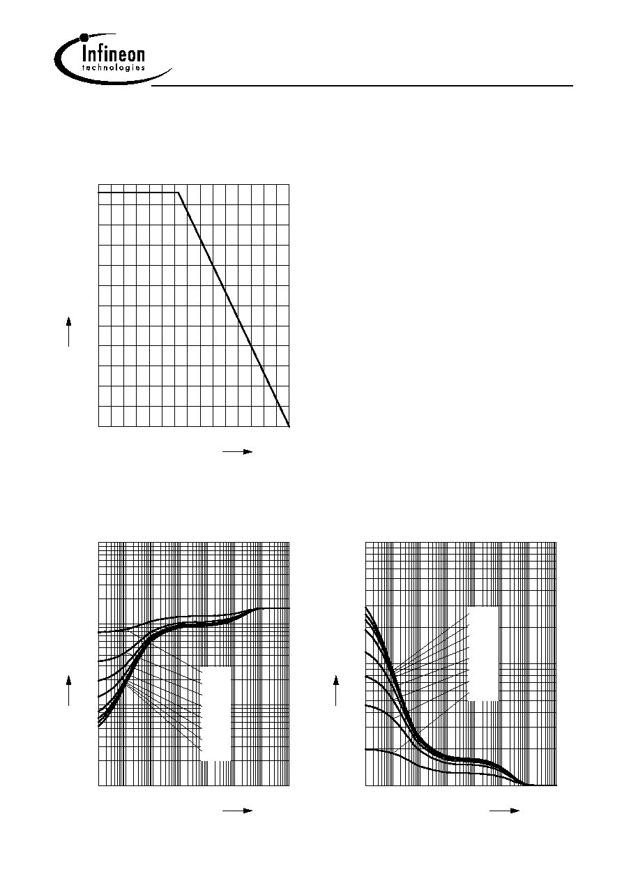
Total power dissipation P
tot
= f (T
S
)
0
20
40
60
80
100
120 �C
150
T
S
0
50
100
150
200
250
300
350
400
450
500
mW
600
P
tot
Permissible Pulse Load R
thJS
= f (t
p
)
10
-7
10
-6
10
-5
10
-4
10
-3
10
-2
10
0
s
t
p
0
10
1
10
2
10
3
10
K/W
R
thJS
0.5
0.2
0.1
0.05
0.02
0.01
0.005
D = 0
Permissible Pulse Load
P
totmax
/P
totDC
= f (t
p
)
10
-7
10
-6
10
-5
10
-4
10
-3
10
-2
10
0
s
t
p
0
10
1
10
2
10
-
P
tot
m
ax
/ P
totDC
D = 0
0.005
0.01
0.02
0.05
0.1
0.2
0.5
BFR193W
Aug-09-2001
6
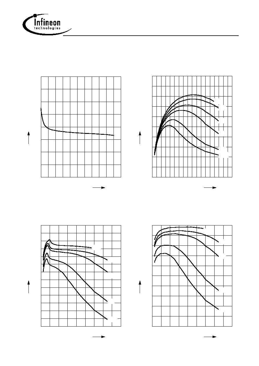
Collector-base capacitance C
cb
= f (V
CB
)
f = 1MHz
0
4
8
12
16
V
22
V
CB
0.0
0.2
0.4
0.6
0.8
1.0
1.2
pF
1.6
C
cb
Transition frequency f
T
= f (I
C
)
V
CE
= Parameter
0
10
20
30
40
50
60
70 mA
90
I
C
0
1
2
3
4
5
6
7
8
GHz
10
f
T
8V
5V
3V
2V
1V
0.7V
Power Gain G
ma
, G
ms
= f(I
C
)
f = 0.9GHz
V
CE
= Parameter
0
10
20
30
40
50
60
70 mA
90
I
C
5
6
7
8
9
10
11
12
13
14
15
16
dB
18
G
10V
3V
1V
0.7V
2V
Power Gain G
ma
, G
ms
= f(I
C
)
f = 1.8GHz
V
CE
= Parameter
0
10
20
30
40
50
60
70 mA
90
I
C
0
1
2
3
4
5
6
7
8
dB
10
G
10V
3V
2V
1V
0.7V
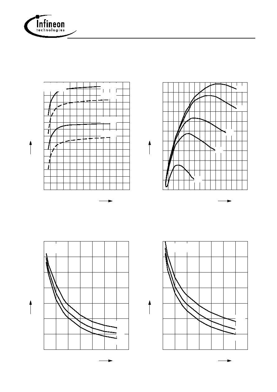
BFR193W
Aug-09-2001
7
Intermodulation Intercept Point IP
3
=f(I
C
)
(3rd order, Output,
Z
S
=Z
L
=50
)
V
CE
= Parameter, f = 900MHz
0
10
20
30
40
50
60
mA
80
I
C
12
14
16
18
20
22
24
26
28
30
dBm
34
IP
3
8V
5V
3V
2V
1V
Power Gain G
ma
, G
ms
= f(V
CE
):_____
|S
21
|
2
= f(V
CE
):---------
f = Parameter
0
2
4
6
8
10
V
13
V
CE
0
2
4
6
8
10
12
dB
16
G
0.9GHz
1.8GHz
0.9GHz
1.8GHz
I
C
=30mA
Power Gain |S
21
|
2
= f(f)
V
CE
=
Parameter
0.0
0.5
1.0
1.5
2.0
2.5
GHz
3.5
f
-5
0
5
10
15
20
dB
30
S
21
10V
1V
0.7V
I
C
=30mA
Power Gain G
ma
, G
ms
= f(f)
V
CE
= Parameter
0.0
0.5
1.0
1.5
2.0
2.5
GHz
3.5
f
0
5
10
15
20
25
dB
35
G
10V
1V
0.7V
I
C
=30mA