BFR280
Jun-27-2001
1
NPN Silicon RF Transistor
For low noise, low-power amplifiers in mobile
communications systems (pager, cordless
telephone) at collector currents from 0.2 mA to 8 m
f
T
= 7.5 GHz
F = 1.5 dB at 900 MHz
1
2
3
VPS05161
ESD
: Electrostatic discharge sensitive device, observe handling precaution!
Type
Marking
Pin Configuration
Package
BFR280
REs
1 = B
2 = E
3 = C
SOT23
Maximum Ratings
Parameter
Symbol
Value
Unit
Collector-emitter voltage
V
CEO
8
V
Collector-emitter voltage
V
CES
10
Collector-base voltage
V
CBO
10
Emitter-base voltage
V
EBO
2
Collector current
I
C
10
mA
Base current
I
B
1.2
Total power dissipation
T
S
116 �C
1)
P
tot
80
mW
Junction temperature
T
j
150
�C
Ambient temperature
T
A
-65 ... 150
Storage temperature
T
stg
-65 ... 150
Thermal Resistance
Junction - soldering point
2)
R
thJS
425
K/W
1T
S
is measured on the collector lead at the soldering point to the pcb
2For calculation of R
thJA
please refer to Application Note Thermal Resistance

BFR280
Jun-27-2001
2
Electrical Characteristics at T
A
= 25�C, unless otherwise specified.
Parameter
Symbol
Values
Unit
min.
typ.
max.
DC characteristics
Collector-emitter breakdown voltage
I
C
= 1 mA, I
B
= 0
V
(BR)CEO
8
-
-
V
Collector-emitter cutoff current
V
CE
= 10 V, V
BE
= 0
I
CES
-
-
100
�A
Collector-base cutoff current
V
CB
= 8 V, I
E
= 0
I
CBO
-
-
100
nA
Emitter-base cutoff current
V
EB
= 1 V, I
C
= 0
I
EBO
-
-
1
�A
DC current gain
I
C
= 3 mA, V
CE
= 5 V
h
FE
30
100
200
-

BFR280
Jun-27-2001
3
Electrical Characteristics at T
A
= 25�C, unless otherwise specified.
Parameter
Symbol
Values
Unit
min.
typ.
max.
AC characteristics
(verified by random sampling)
Transition frequency
I
C
= 6 mA, V
CE
= 5 V, f = 500 MHz
f
T
5
7.5
-
GHz
Collector-base capacitance
V
CB
= 5 V, f = 1 MHz
C
cb
-
0.27
0.45
pF
Collector-emitter capacitance
V
CE
= 5 V, f = 1 MHz
C
ce
-
0.18
-
Emitter-base capacitance
V
EB
= 0.5 V, f = 1 MHz
C
eb
-
0.22
-
Noise figure
I
C
= 1.5 mA, V
CE
= 5 V, Z
S
= Z
Sopt
,
f
= 900 MHz
f
= 1.8 GHz
F
-
-
1.5
2
-
-
dB
Power gain, maximum stable
1)
I
C
= 3 mA, V
CE
= 5 V, Z
S
= Z
Sopt
, Z
L
= Z
Lopt
,
f
= 900 MHz
f
= 1.8 GHz
G
ms
-
-
17
11.5
-
-
Transducer gain
I
C
= 3 mA, V
CE
= 5 V, Z
S
= Z
L
= 50
,
f
= 900 MHz
f
= 1.8 GHz
|S
21e
|
2
-
-
13
8
-
-
1
G
ms
= |S
21
/ S
12
|
BFR280
Jun-27-2001
4
SPICE Parameters (Gummel-Poon Model, Berkley-SPICE 2G.6 Syntax) :
Transistor Chip Data
IS =
6.472
fA
VAF =
25.609
V
NE =
1.6163
-
VAR =
5.6909
V
NC =
1.0651
-
RBM =
14.999
CJE =
36.218
fF
TF =
11.744
ps
ITF =
6.2179
mA
VJC =
1.1943
V
TR =
2.3693
ns
MJS =
0
-
XTI =
3
-
BF =
89.888
-
IKF =
0.073457
A
BR =
20.238
-
IKR =
0.012696
A
RB =
15
RE =
2.4518
VJE =
0.70035
V
XTF =
0.21585
-
PTF =
0
deg
MJC =
0.30017
-
CJS =
0
fF
XTB =
0
-
FC =
0.96275
-
NF =
1.0801
-
ISE =
15.596
fA
NR =
0.83403
-
ISC =
1.409
fA
IRB =
0.031958
mA
RC =
6.989
MJE =
0.69773
-
VTF =
0.2035
V
CJC =
252.99
fF
XCJC =
0.19188
-
VJS =
0.75
V
EG =
1.11
eV
TNOM
300
K
All parameters are ready to use, no scalling is necessary.
Extracted on behalf of Infineon Technologies AG by:
Institut f�r Mobil-und Satellitentechnik (IMST)
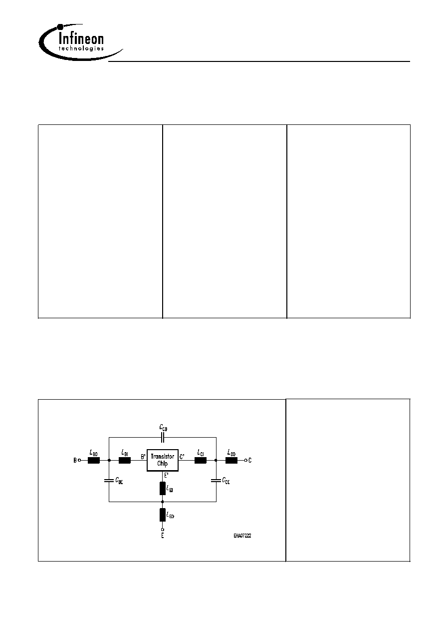
Package Equivalent Circuit:
L
BI
=
0.85
nH
L
BO
=
0.51
nH
L
EI
=
0.69
nH
L
EO
=
0.61
nH
L
CI
=
0
nH
L
CO
=
0.49
nH
C
BE
=
73
fF
C
CB
=
84
fF
C
CE
=
165
fF
Valid up to 6GHz
For examples and ready to use parameters please contact your local Infineon Technologies distributor or sales
office to obtain a Infineon Technologies CD-ROM or see Internet: http://www.infineon.com/products/discrete/index.htm
BFR280
Jun-27-2001
5
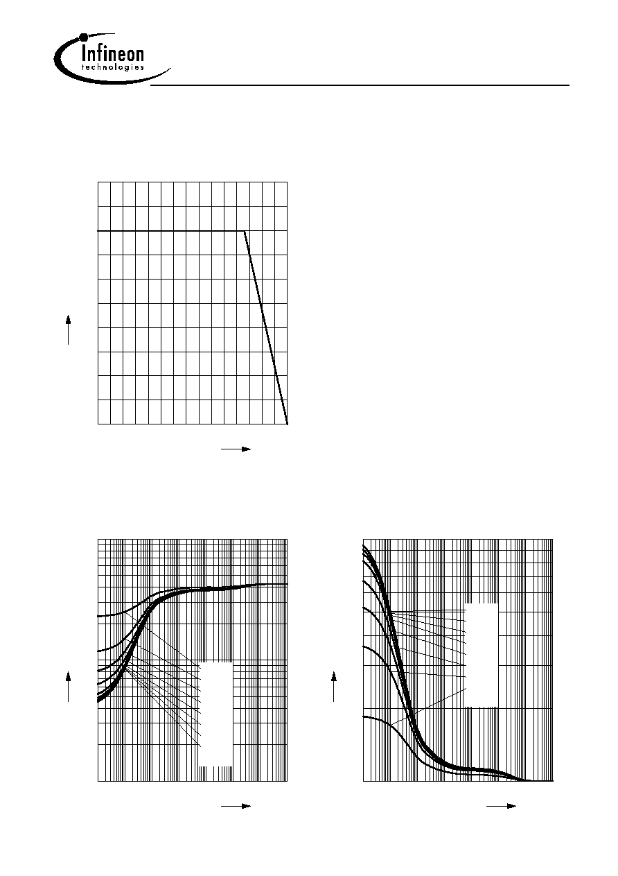
Total power dissipation
P
tot
= f (T
S
)
0
20
40
60
80
100
120 �C
150
T
S
0
10
20
30
40
50
60
70
80
mW
100
P
tot
Permissible Pulse Load
R
thJS
= f (t
p
)
10
-7
10
-6
10
-5
10
-4
10
-3
10
-2
10
0
s
t
p
1
10
2
10
3
10
K/W
R
thJS
0.5
0.2
0.1
0.05
0.02
0.01
0.005
D = 0
Permissible Pulse Load
P
totmax
/P
totDC
= f (t
p
)
10
-7
10
-6
10
-5
10
-4
10
-3
10
-2
10
0
s
t
p
0
10
1
10
-
P
totmax
/ P
totDC
D = 0
0.005
0.1
0.2
0.05
0.1
0.2
0.5
BFR280
Jun-27-2001
6
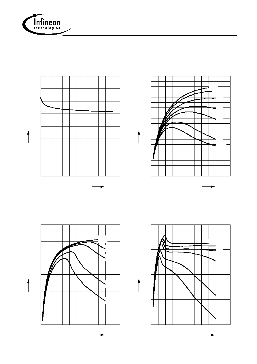
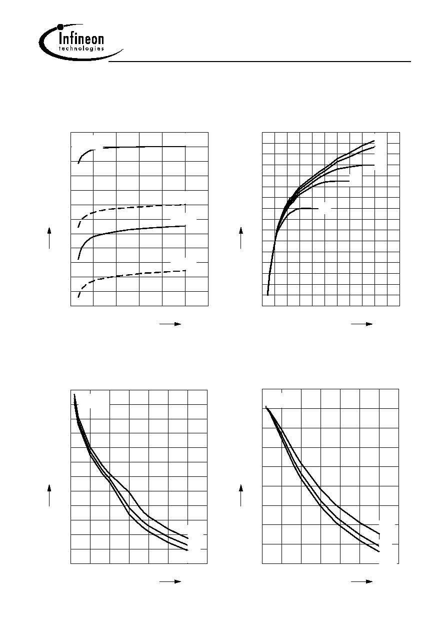
Collector-base capacitance
C
cb
= f (V
CB
)
f = 1MHz
0
2
4
6
8
V
11
V
CB
0
0.05
0.1
0.15
0.2
0.25
0.3
pF
0.4
C
cb
Transition frequency
f
T
= f (I
C
)
V
CE
= Parameter
0
2
4
6
8
mA
11
I
C
0
1
2
3
4
5
6
7
8
GHz
9.5
f
T
10V
8V
5V
3V
2V
1V
0.7V
Power Gain
G
ma
, G
ms
= f(I
C
)
f = 0.9GHz
V
CE
= Parameter
0
2
4
6
8
mA
11
I
C
8
10
12
14
16
dB
20
G
10V
3V
3V
2V
0.7V
Power Gain
G
ma
, G
ms
= f(I
C
)
f = 1.8GHz
V
CE
= Parameter
0
2
4
6
8
mA
11
I
C
5
6
7
8
9
10
11
dB
13
G
10V
5V
3V
2V
1V
0.7V
BFR280
Jun-27-2001
7
Intermodulation Intercept Point
IP
3
=f(I
C
)
(3rd order, Output,
Z
S
=Z
L
=50
)
V
CE
= Parameter, f = 900MHz
0
2
4
6
8
mA
11
I
C
-12
-8
-4
0
4
8
12
dBm
20
IP
3
8V
5V
3V
2V
1V
Power Gain
G
ma
, G
ms
= f(V
CE
):_____
|S
21
|
2
= f(V
CE
):---------
f = Parameter
0
2
4
6
8
V
12
V
CE
6
7
8
9
10
11
12
13
14
15
16
dB
18
G
0.9GHz
1.8GHz
0.9GHz
1.8GHz
I
C
=3mA
Power Gain
|S
21
|
2
= f(f)
V
CE
=
Parameter
0
0.5
1
1.5
2
2.5
GHz
3.5
f
2
4
6
8
10
12
14
16
dB
20
S
21
10V
1V
0.7V
I
C
=3mA
Power Gain
G
ma
, G
ms
= f(f)
V
CE
= Parameter
0
0.5
1
1.5
2
2.5
GHz
3.5
f
4
6
8
10
12
14
16
18
20
22
24
dB
28
G
10V
1V
0.7V
I
C
=3mA