BFR92T
Aug-08-2001
1
NPN Silicon RF Transistor
Preliminary data
For broadband amplifiers up to 2 GHz and
fast non-saturated switches at collector currents
from 0.5 mA to 20 mA
Complementary type: BFT92T (PNP)
VPS05996
1
2
3
ESD: Electrostatic discharge sensitive device, observe handling precaution!
Type
Marking
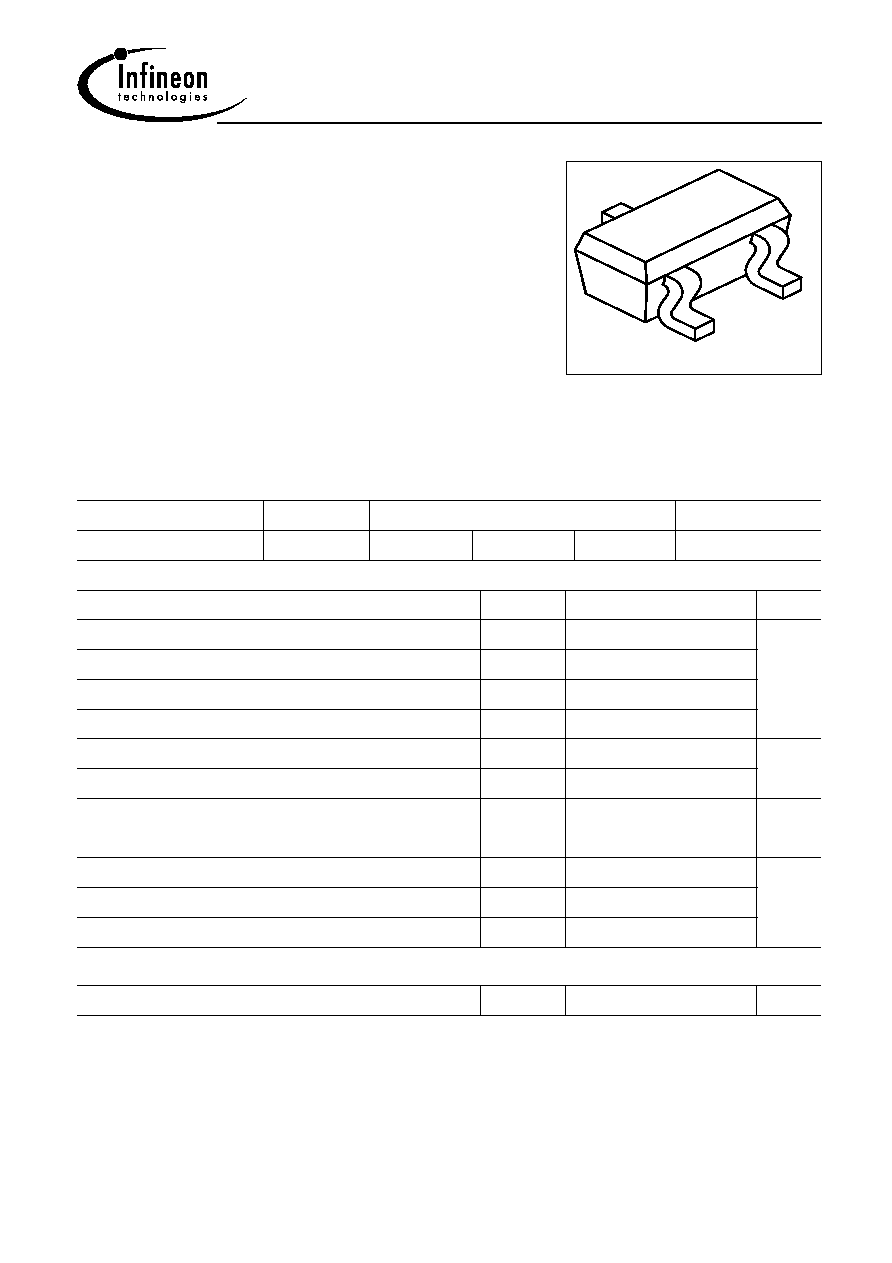
Pin Configuration
Package
BFR92T
GFs
1 = B
2 = E
3 = C
SC75
Maximum Ratings
Parameter
Symbol
Value
Unit
Collector-emitter voltage
V
CEO
15
V
Collector-emitter voltage
V
CES
20
Collector-base voltage
V
CBO
20
Emitter-base voltage
V
EBO
2.5
Collector current
I
C
30
mA
Base current
I
B
4
Total power dissipation
T
S
69�C
1)
P
tot
280
mW
Junction temperature
T
j
150
�C
Ambient temperature
T
A
-65 ... 150
Storage temperature
T
stg
-65 ... 150
Thermal Resistance
Junction - soldering point
2)
R
thJS
290
K/W
1T
S
is measured on the collector lead at the soldering point to the pcb
2For calculation of R
thJA
please refer to Application Note Thermal Resistance

BFR92T
Aug-08-2001
2
Electrical Characteristics at T
A
= 25�C, unless otherwise specified.
Parameter
Symbol
Values
Unit
min.
typ.
max.
DC characteristics
Collector-emitter breakdown voltage
I
C
= 1 mA, I
B
= 0
V
(BR)CEO
15
-
-
V
Collector-emitter cutoff current
V
CE
= 20 V, V
BE
= 0
I
CES
-
-
10
�A
Collector-base cutoff current
V
CB
= 10 V, I
E
= 0
I
CBO
-
-
100
nA
Emitter-base cutoff current
V
EB
= 2.5 V, I
C
= 0
I
EBO
-
-
100
�A
DC current gain
I
C
= 15 mA, V
CE
= 8 V
h
FE
40
100
200
-

BFR92T
Aug-08-2001
3
Electrical Characteristics at T
A
= 25�C, unless otherwise specified.
Parameter
Symbol
Values
Unit
min.
typ.
max.
AC characteristics
(verified by random sampling)
Transition frequency
I
C
= 15 mA, V
CE
= 8 V, f = 500 MHz
f
T
3.5
5
-
GHz
Collector-base capacitance
V
CB
= 10 V, f = 1 MHz
C
cb
-
0.38
0.6
pF
Collector-emitter capacitance
V
CE
= 10 V, f = 1 MHz
C
ce
-
0.2
-
Emitter-base capacitance
V
EB
= 0.5 V, f = 1 MHz
C
eb
-
0.7
-
Noise figure
I
C
= 2 mA, V
CE
= 6 V, Z
S
= Z
Sopt
,
f
= 900 MHz
f
= 1.8 GHz
F
-
-
1.8
2.9
-
-
dB
Power gain, maximum available
1)
I
C
= 15 mA, V
CE
= 8 V, Z
S
= Z
Sopt
, Z
L
= Z
Lopt
,
f
= 900 MHz
f
= 1.8 GHz
G
ma
-
-
16
10.5
-
-
Transducer gain
I
C
= 15 mA, V
CE
= 8 V, Z
S
= Z
L
= 50
,
f
= 900 MHz
f
= 1.8 GHz
|S
21e
|
2
-
-
13.5
8
-
-
1
G
ma
= |S
21
/ S
12
| (k-(k
2
-1)
1/2
)
BFR92T
Aug-08-2001
4
SPICE Parameters (Gummel-Poon Model, Berkley-SPICE 2G.6 Syntax) :
Transistor Chip Data
IS =
0.1213
fA
VAF =
30
V
NE =
1.9052
-
VAR =
14.599
V
NC =
1.371
-
RBM =
7.8145
CJE =
10.416
fF
TF =
26.796
ps
ITF =
4.4601
mA
VJC =
0.84079
V
TR =
1.2744
ns
MJS =
0
-
XTI =
3
-
BF =
94.733
-
IKF =
0.46227
A
BR =
10.729
-
IKR =
0.01
A
RB =
14.998
RE =
0.29088
VJE =
0.70618
V
XTF =
0.3817
-
PTF =
0
deg
MJC =
0.4085
-
CJS =
0
fF
XTB =
0
-
FC =
0.99545
-
NF =
1.0947
-
ISE =
129.55
fA
NR =
0.8983
-
ISC =
0.75557
fA
IRB =
0.01652
mA
RC =
0.13793
MJE =
0.34686
-
VTF =
0.32861
V
CJC =
946.47
fF
XCJC =
0.13464
-
VJS =
0.75
V
EG =
1.11
eV
TNOM
300
K
All parameters are ready to use, no scalling is necessary.
Extracted on behalf of Infineon Technologies AG by:
Institut f�r Mobil-und Satellitentechnik (IMST)
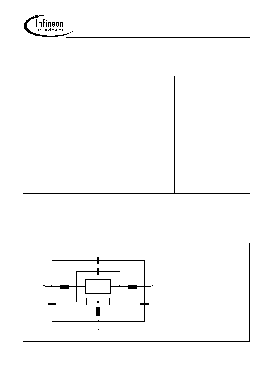
Package Equivalent Circuit:
L
1
=
0.762
nH
L
2
=
0.706
nH
L
3
=
0.382
nH
C
1
62
fF
C
2
84
fF
C
3
180
fF
C
4
=
7
C
5
=
40
fF
C
6
=
48
fF
EHA07524
Transistor
C'
L
E'
B'
3
4
C
C
Chip
E
L
1
5
C
B
2
L
C
6
C
1
C
2
C
3
Valid up to 6GHz
For examples and ready to use parameters please contact your local Infineon Technologies distributor or sales
office to obtain a Infineon Technologies CD-ROM or see Internet: http://www.infineon.com/silicondiscretes
BFR92T
Aug-08-2001
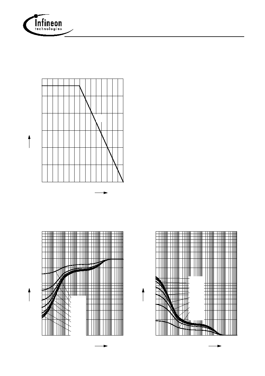
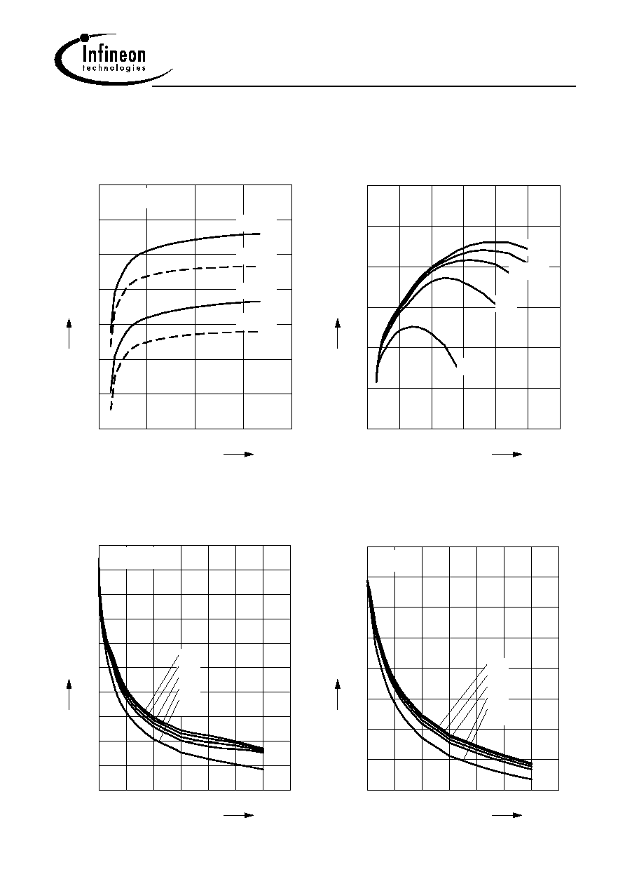
5
Total power dissipation P
tot
= f (T
S
)
0
20
40
60
80
100
120 �C
150
T
S
0
50
100
150
200
mW
300
P
tot
TS
Permissible Pulse Load R
thJS
= f (t
p
)
10
-7
10
-6
10
-5
10
-4
10
-3
10
-2
10
0
s
t
p
1
10
2
10
3
10
R
thJS
D=0.5
0.2
0.1
0.05
0.02
0.01
0.005
0
Permissible Pulse Load
P
totmax
/P
totDC
= f (t
p
)
10
-7
10
-6
10
-5
10
-4
10
-3
10
-2
10
0
s
t
p
0
10
1
10
2
10
P
totmax
/ P
totDC
D=0
0.005
0.01
0.02
0.05
0.1
0.2
0.5
BFR92T
Aug-08-2001
6
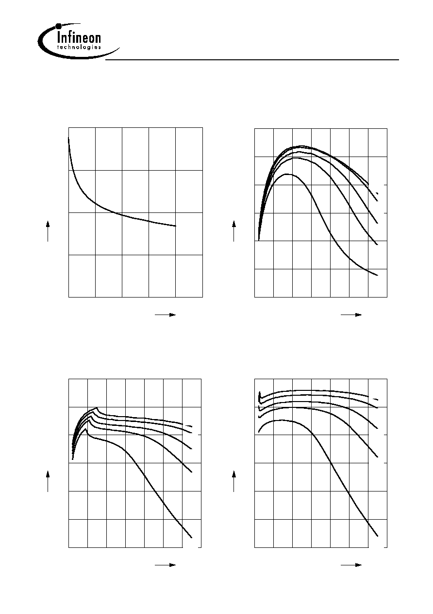
Collector-base capacitance C
cb
= f (V
CB
)
f = 1MHz
0
5
10
15
V
25
V
CB
0
0.2
0.4
pF
0.8
C
cb
Transition frequency f
T
= f (I
C
)
V
CE
= Parameter
0
5
10
15
20
25
mA
35
I
C
0
1
2
3
4
GHz
6
f
T
8V
5V
3V
2V
1V
Power Gain G
ma
, G
ms
= f(I
C
)
f = 0.9GHz
V
CE
= Parameter
0
5
10
15
20
25
mA
35
I
C
-2
2
6
10
14
dB
22
G
8V
5V
3V
2V
1V
Power Gain G
ma
, G
ms
= f(I
C
)
f = 1.8GHz
V
CE
= Parameter
0
5
10
15
20
25
mA
35
I
C
-6
-3
0
3
6
dB
12
G
ma
8V
5V
3V
2V
1V
BFR92T
Aug-08-2001
7
Intermodulation Intercept Point IP
3
=f(I
C
)
(3rd order, Output,
Z
S
=Z
L
=50
)
V
CE
= Parameter, f = 900MHz
0
5
10
15
20
mA
30
I
C
0
5
10
15
20
dBm
30
IP
3
5V
4V
3V
2V
1V
Power Gain G
ma
, G
ms
= f(V
CE
):_____
|S
21
|
2
= f(V
CE
):---------
f = Parameter
0
3
6
V
12
V
CE
0
3
6
9
12
15
dB
21
G
0.9GHz
1.8GHz
0.9GHz
1.8GHz
I
C
=15mA
Power Gain |S
21
|
2
= f(f)
V
CE
=
Parameter
0
1
2
3
4
5
GHz
7
f
-5
0
5
10
15
20
25
dBm
35
S
21
I
C
=15mA
8V
5V
3V
2V
1V
Power Gain G
ma
, G
ms
= f(f)
V
CE
= Parameter
0
1
2
3
4
5
GHz
7
f
-5
0
5
10
15
20
25
30
35
dB
45
G
I
C
=15mA
8V
5V
3V
2V
1V