 | –≠–ª–µ–∫—Ç—Ä–æ–Ω–Ω—ã–π –∫–æ–º–ø–æ–Ω–µ–Ω—Ç: BFY182H | –°–∫–∞—á–∞—Ç—å:  PDF PDF  ZIP ZIP |

BFY182
Semiconductor Group
1 of 5
Draft B, September 1999
HiRel NPN Silicon RF Transistor
∑
HiRel Discrete and Microwave Semiconductor
∑
For low noise, high-gain broadband amplifiers at collector
currents from 1 mA to 20 mA.
∑
Hermetically sealed microwave package
∑
f
T
= 8 GHz
F = 2.4 dB at 2 GHz
∑
Space Qualified
ESA/SCC Detail Spec. No.: 5611/006
Type Variant No. 04
ESD: Electrostatic discharge sensitive device,
observe handling precautions!
Type
Marking
Ordering Code
Pin Configuration
Package
BFY182 (ql)
-
see below
C
E
B
E
Micro-X1
(ql) Quality Level:
P: Professional Quality,
Ordering Code:
Q62702F1608
H: High Rel Quality,
Ordering Code:
on request
S: Space Quality,
Ordering Code:
on request
ES: ESA Space Quality,
Ordering Code:
Q62702F1714
(see order instructions for ordering example)
1
2
3
4
BFY182
Semiconductor Group
2 of 5
Draft B, September 1999
Maximum Ratings
Parameter
Symbol
Values
Unit
Collector-emitter voltage
V
CEO
12
V
Collector-emitter voltage, V
BE
=0
V
CES
20
V
Collector-base voltage
V
CBO
20
V
Emitter-base voltage
V
EBO
2
V
Collector current
I
C
35
mA
Base current
I
B
4
1)
mA
Total power dissipation,
T
S
136∞C
2), 3.)
P
tot
250
mW
Junction temperature
T
j
200
∞
C
Operating temperature range
T
op
-65...+200
∞
C
Storage temperature range
T
stg
-65...+200
∞
C
Thermal Resistance
Junction-soldering point
3.)
R
th JS
< 255
K/W
Notes.:
1) The maximum permissible base current for V
FBE
measurements is 20mA (spot-
measurement duration < 1s)
2) At T
S
= + 136 ∞C. For T
S
> + 136 ∞C derating is required.
3) T
S
is measured on the collector lead at the soldering point to the pcb.
Electrical Characteristics
at T
A
=25∞C; unless otherwise specified
Parameter
Symbol
Values
Unit
min.
typ.
max.
DC Characteristics
Collector-base cutoff current
V
CB
= 20 V, I
E
= 0
I
CBO
-
-
100
µA
Collector-emitter cutoff current
V
CE
= 12 V, I
B
= 0.2µA
1.)
I
CEX
-
-
200
µA
Collector-base cutoff current
V
CB
= 10 V, I
E
= 0
I
CBO
-
-
50
nA
Emitter base cuttoff current
V
EB
= 2 V, I
C
= 0
I
EBO
-
-
25
µ
A
Emitter base cuttoff current
V
EB
= 1 V, I
C
= 0
I
EBO
-
-
0.5
µ
A
Notes:
1.) This Test assures V(BR)
CE0
> 12V
BFY182
Semiconductor Group
3 of 5
Draft B, September 1999
Electrical Characteristics (continued)
Parameter
Symbol
Values
Unit
min.
typ.
max.
DC Characteristics
Base-Emitter forward voltage
I
E
= 20 mA, I
C
= 0
V
FBE
-
-
1
V
DC current gain
I
C
= 5 mA, V
CE
= 6 V
h
FE
55
100
170
-
AC Characteristics
Transition frequency
I
C
= 15 mA, V
CE
= 5 V, f = 500 MHz
I
C
= 15 mA, V
CE
= 8 V, f = 500 MHz
f
T
6.5
-
7.5
8
-
-
GHz
Collector-base capacitance
V
CB
= 10 V, V
BE
= vbe = 0, f = 1 MHz
C
CB
-
0.26
0.36
pF
Collector-emitter capacitance
V
CE
= 10 V, V
BE
= vbe = 0, f = 1 MHz
C
CE
-
0.34
-
pF
Emitter-base capacitance
V
EB
= 0.5V, V
CB
= vcb = 0, f = 1 MHz
C
EB
-
0.8
1.1
pF
Noise Figure
I
C
= 5 mA, V
CE
= 5 V, f = 2 GHz,
Z
S
= Z
Sopt
F
-
2.4
2.9
dB
Power gain
I
C
= 15 mA, V
CE
= 5V, f = 2 GHz
Z
S
= Z
Sopt
, Z
L
= Z
Lopt
Gma
1.)
13.5
14.5
-
dB
Transducer gain
I
C
= 15 mA, V
CE
= 5 V, f = 2 GHz
Z
S
= Z
L
= 50
|S
21e
|
2
10
11
-
dB
Notes.:
1)
G
S
S
k
k
ma
=
-
-
21
12
1
2
(
)
,
G
S
S
ms
=
21
12

BFY182
Semiconductor Group
4 of 5
Draft B, September 1999
Order Instructions:
Full type variant including quality level must be specified by the orderer. For HiRel Discrete
and Microwave Semiconductors the ordering code specifies device family and quality level.
Ordering Form:
Ordering Code: Q..........
BFY182 (ql)
(ql): Quality Level
Ordering Example:
Ordering Code:
Q62702F1714
BFY182 ES
For BFY182 in ESA Space Quality Level
Further Informations:
See our WWW-Pages:
- Discrete and RF-Semiconductors (Small Signal Semiconductors)
www.infineon.com/products/discrete/hirel.htm
- HiRel Discrete and Microwave Semiconductors
www.infineon.com/products/discrete/hirel.htm
Please contact also our marketing division :
Tel.:
++89 234 24480
Fax.:
++89 234 28438
e-mail:
martin.wimmers@infineon.com
Address:
Infineon -Technologies Semiconductors,
High Frequency Products Marketing,
P.O.Box 801709,
D-81617 Munich
BFY182
Semiconductor Group
5 of 5
Draft B, September 1999
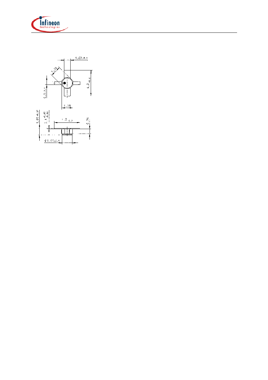
Micro-X1 Package
1
2
3
4
Published by Infineon Technologies Semiconductors,
High Frequency Products Marketing, P.O.Box 801709,
D-81617 Munich.
Infineon Technologies AG 1998. All Rights Reserved.
As far as patents or other rights of third parties are
concerned, liability is only assumed for components per
se, not for applications, processes and circuits
implemented within components or assemblies.
The information describes the type of component and shall
not be considered as assured characteristics.
Terms of delivery and rights to change design reserved.
For questions on technology, delivery and prices please
contact the Offices of Semiconductor Group in Germany or
the Infineon Technologies Companies and
Representatives woldwide (see address list).
Due to technical requirements components may contain
dangerous substances. For information on the type in
question please contact your nearest Infineon
Technologies Office, Semiconductor Group.
Infineon Technologies Semiconductors is a certified CECC
and QS9000 manufacturer (this includes ISO 9000).