
BPX 38
NPN-Silizium-Fototransistor
Silicon NPN Phototransistor
2001-02-21
1
Features
∑ Especially suitable for applications from
450 nm to 1120 nm
∑ High linearity
∑ Hermetically sealed metal package (TO-18)
with base connection, suitable up to 125
∞
C
∑ Available in groups
Applications
∑ Photointerrupters
∑ Industrial electronics
∑ For control and drive circuits
Wesentliche Merkmale
∑ Speziell geeignet f¸r Anwendungen im Bereich
von 450 nm bis 1120 nm
∑ Hohe Linearit‰t
∑ Hermetisch dichte Metallbauform (TO-18) mit
Basisanschluþ, geeignet bis 125
∞
C
∑ Gruppiert lieferbar
Anwendungen
∑ Lichtschranken f¸r Gleich- und
Wechsellichtbetrieb
∑ Industrieelektronik
∑ ,,Messen/Steuern/Regeln"
Typ
Type
Bestellnummer
Ordering Code
Typ
Type
Bestellnummer
Ordering Code
BPX 38
Q62702-P15
BPX 38-4
Q62702-P15-S4
BPX 38-2/3
Q62702-P3578
BPX 38-4/5
Q62702-P5197
BPX 38-3
Q62702-P15-S3
BPX 38-5
1)
1)
Eine Lieferung in dieser Gruppe kann wegen Ausbeuteschwankungen nicht immer sichergestellt werden.
Wir behalten uns in diesem Fall die Lieferung einer Ersatzgruppe vor.
1)
Supplies out of this group cannot always be guaranteed due to unforseeable spread of yield.
In this case we will reserve us the right of delivering a substitute group.
Q62702-P15-S5
BPX 38-3/4
Q62702-P3579
2001-02-21
2
BPX 38
Grenzwerte
Maximum Ratings
Bezeichnung
Parameter
Symbol
Symbol
Wert
Value
Einheit
Unit
Betriebs- und Lagertemperatur
Operating and storage temperature range
T
op
;
T
stg
≠ 40 ... + 125
∞
C
Lˆttemperatur bei Tauchlˆtung
Lˆtstelle
2 mm vom Geh‰use,
Lˆtzeit
t
5 s
Dip soldering temperature
2 mm distance
from case bottom, soldering time
t
5 s
T
S
260
∞
C
Lˆttemperatur bei Kolbenlˆtung
Lˆtstelle
2 mm vom Geh‰use,
Lˆtzeit
t
3 s
Iron soldering temperature
2 mm distance
from case bottom, soldering time
t
3 s
T
S
300
∞
C
Kollektor-Emitterspannung
Collector-emitter voltage
V
CE
50
V
Kollektorstrom
Collector current
I
C
50
mA
Kollektorspitzenstrom,
<
10
µ
s
Collector surge current
I
CS
200
mA
Emitter-Basisspannung
Emitter-base voltage
V
EB
7
V
Verlustleistung,
T
A
= 25
∞
C
Total power dissipation
P
tot
220
mW
W‰rmewiderstand
Thermal resistance
R
thJA
450
K/W
BPX 38
2001-02-21
3
Kennwerte (
T
A
= 25
∞
C,
= 950 nm)
Characteristics
Bezeichnung
Parameter
Symbol
Symbol
Wert
Value
Einheit
Unit
Wellenl‰nge der max. Fotoempfindlichkeit
Wavelength of max. sensitivity
S max
880
nm
Spektraler Bereich der Fotoempfindlichkeit
S
= 10% von
S
max
Spectral range of sensitivity
S
= 10% of
S
max
450 ... 1120
nm
Bestrahlungsempfindliche Fl‰che
Radiant sensitive area
A
0.675
mm
2
Abmessung der Chipfl‰che
Dimensions of chip area
L
◊
B
L
◊
W
1
◊
1
mm
◊
mm
Abstand Chipoberfl‰che zu Geh‰useoberfl‰che
Distance chip front to case surface
H
2.05 ... 2.35
mm
Halbwinkel
Half angle
±
40
Grad
deg.
Fotostrom der Kollektor-Basis-Fotodiode
Photocurrent of collector-base photodiode
E
e
= 0.5 mW/cm
2
,
V
CB
= 5 V
E
v
= 1000 Ix, Normlicht/standard light A,
V
CB
= 5 V
I
PCB
I
PCB
1.8
5.5
µ
A
µ
A
Kapazit‰t
Capacitance
V
CE
= 0 V,
f
= 1 MHz,
E
= 0
V
CB
= 0 V,
f
= 1 MHz,
E
= 0
V
EB
= 0 V,
f
= 1 MHz,
E
= 0
C
CE
C
CB
C
EB
23
39
47
pF
pF
pF
Dunkelstrom
Dark current
V
CE
= 25 V,
E
= 0
I
CEO
20 (
300)
nA
2001-02-21
4
BPX 38
Die Fototransistoren werden nach ihrer Fotoempfindlichkeit gruppiert und mit arabischen Ziffern
gekennzeichnet.
The phototransistors are grouped according to their spectral sensitivity and distinguished by
arabian figures.
Bezeichnung
Parameter
Symbol
Symbol
Wert
Value
Einh.
Unit
-2
-3
-4
-5
Fotostrom,
=
950 nm
Photocurrent
E
e
= 0.5 mW/cm
2
,
V
CE
= 5 V
E
v
= 1000 Ix, Normlicht/standard light A,
V
CE
= 5 V
I
PCE
I
PCE
0.2 ... 0.4
0.95
0.32 ... 0.63
1.5
0.5 ... 1.0
2.3
0.8
3.6
mA
mA
Anstiegszeit/Abfallzeit
Rise and fall time
I
C
= 1 mA,
V
CC
= 5 V,
R
L
= 1 k
t
r
,
t
f
9
12
15
18
µ
s
Kollektor-Emitter-S‰ttigungsspannung
Collector-emitter saturation voltage
I
C
=
I
PCEmin
1)
◊
0.3
E
e
= 0.5 mW/cm
2
V
CEsat
200
200
200
200
mV
Stromverst‰rkung
Current gain
E
e
= 0.5 mW/cm
2
,
V
CE
= 5 V
170
280
420
650
≠
1)
I
PCEmin
ist der minimale Fotostrom der jeweiligen Gruppe.
1)
I
PCEmin
is the min. photocurrent of the specified group.
I
PCE
I
PCB
-----------
BPX 38
2001-02-21
5
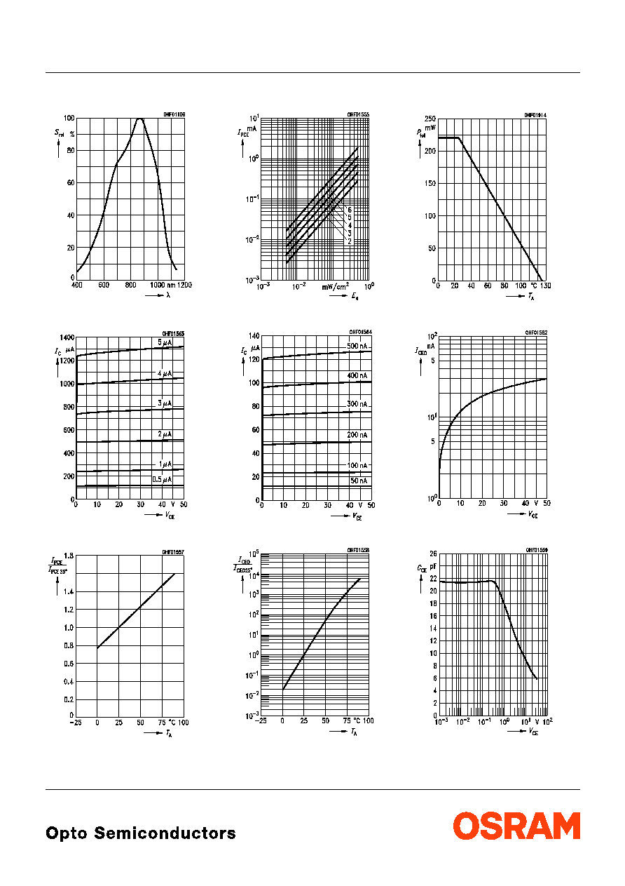
Relative Spectral Sensitivity
S
rel
=
f
(
)
Output Characteristics
I
C
=
f
(
V
CE
),
I
B
= Parameter
Photocurrent
I
PCE
/
I
PCE25
o
=
f
(
T
A
),
V
CE
= 5 V
Photocurrent
I
PCE
=
f
(
E
e
),
V
CE
= 5 V
Output Characteristics
I
C
=
f
(
V
CE
),
I
B
= Parameter
Dark Current
I
CEO
/
I
CEO25
o
=
f
(
T
A
),
V
CE
= 25 V,
E
= 0
Total Power Dissipation
P
tot
=
f
(
T
A
)
Dark Current
I
CEO
=
f
(
V
CE
),
E
= 0
Collector-Emitter Capacitance
C
CE
=
f
(
V
CE
),
f
= 1 MHz,
E
= 0
BPX 38
2001-02-21
6
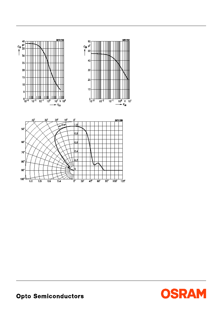
Collector-Base Capacitance
C
CB
=
f
(
V
CB
),
f
= 1 MHz,
E
= 0
Directional Characteristics
S
rel
=
f
(
)
Emitter-Base Capacitance
C
EB
=
f
(
V
EB
),
f
= 1 MHz,
E
= 0

BPX 38
2001-02-21
7
Maþzeichnung
Package Outlines
Maþe werden wie folgt angegeben: mm (inch) / Dimensions are specified as follows: mm (inch).
Published by OSRAM Opto Semiconductors GmbH & Co. OHG
Wernerwerkstrasse 2, D-93049 Regensburg
© All Rights Reserved.
Attention please!
The information describes the type of component and shall not be considered as assured characteristics.
Terms of delivery and rights to change design reserved. Due to technical requirements components may contain
dangerous substances. For information on the types in question please contact our Sales Organization.
Packing
Please use the recycling operators known to you. We can also help you ≠ get in touch with your nearest sales office.
By agreement we will take packing material back, if it is sorted. You must bear the costs of transport. For packing
material that is returned to us unsorted or which we are not obliged to accept, we shall have to invoice you for any costs
incurred.
Components used in life-support devices or systems must be expressly authorized for such purpose! Critical
components
1
, may only be used in life-support devices or systems
2
with the express written approval of OSRAM OS.
1
A critical component is a component usedin a life-support device or system whose failure can reasonably be expected
to cause the failure of that life-support device or system, or to affect its safety or effectiveness of that device or system.
2
Life support devices or systems are intended (a) to be implanted in the human body, or (b) to support and/or maintain
and sustain human life. If they fail, it is reasonable to assume that the health of the user may be endangered.
¯5.6 (0.220)
¯5.3 (0.209)
2.54 (0.100)
spacing
¯
4.8 (0.189)
E C B
(2.7 (0.106))
5.3 (0.209)
5.0 (0.197)
14.5 (0.571)
12.5 (0.492)
¯0.45 (0.018)
Radiant
GMOY6018
Approx. weight 1.0 g
¯
4.6 (0.181)
5.0 (0.197)
5.5 (0.217)
Chip position
sensitive area
0.9 (0.035)
1.1 (0.043)
1.1 (0.043)
0.9 (0.035)