BSC027N03S G
Opti
MOS
ģ
2 Power-Transistor
Features
∑ Fast switching MOSFET for SMPS
∑ Optimized technology for notebook DC/DC converters
∑ Qualified according to JEDEC
1
for target applications
∑ Logic level / N-channel
∑ Excellent gate charge x R
DS(on)
product (FOM)
∑ Very low on-resistance R
DS(on)
∑ Superior thermal resistance
∑ Avalanche rated
∑ dv /dt rated
∑ Pb-free lead plating; RoHS compliant
Maximum ratings, at T
j
=25 įC, unless otherwise specified
Parameter
Symbol Conditions
Unit
Continuous drain current
I
D
T
C
=25 įC
100
A
T
C
=100 įC
90
T
A
=25 įC,
R
thJA
=45 K/W
2)
25
Pulsed drain current
I
D,pulse
T
C
=25 įC
3)
200
Avalanche energy, single pulse
E
AS
I
D
=50 A, R
GS
=25
800
mJ
Reverse diode dv /dt
dv /dt
I
D
=50 A, V
DS
=24 V,
di /dt =200 A/Ķs,
T
j,max
=150 įC
6
kV/Ķs
Gate source voltage
V
GS
Ī20
V
Power dissipation
P
tot
T
C
=25 įC
89
W
T
A
=25 įC,
R
thJA
=45 K/W
2)
2.8
Operating and storage temperature
T
j
, T
stg
-55 ... 150
įC
IEC climatic category; DIN IEC 68-1
55/150/56
Value
V
DS
30
V
R
DS(on),max
2.7
m
I
D
100
A
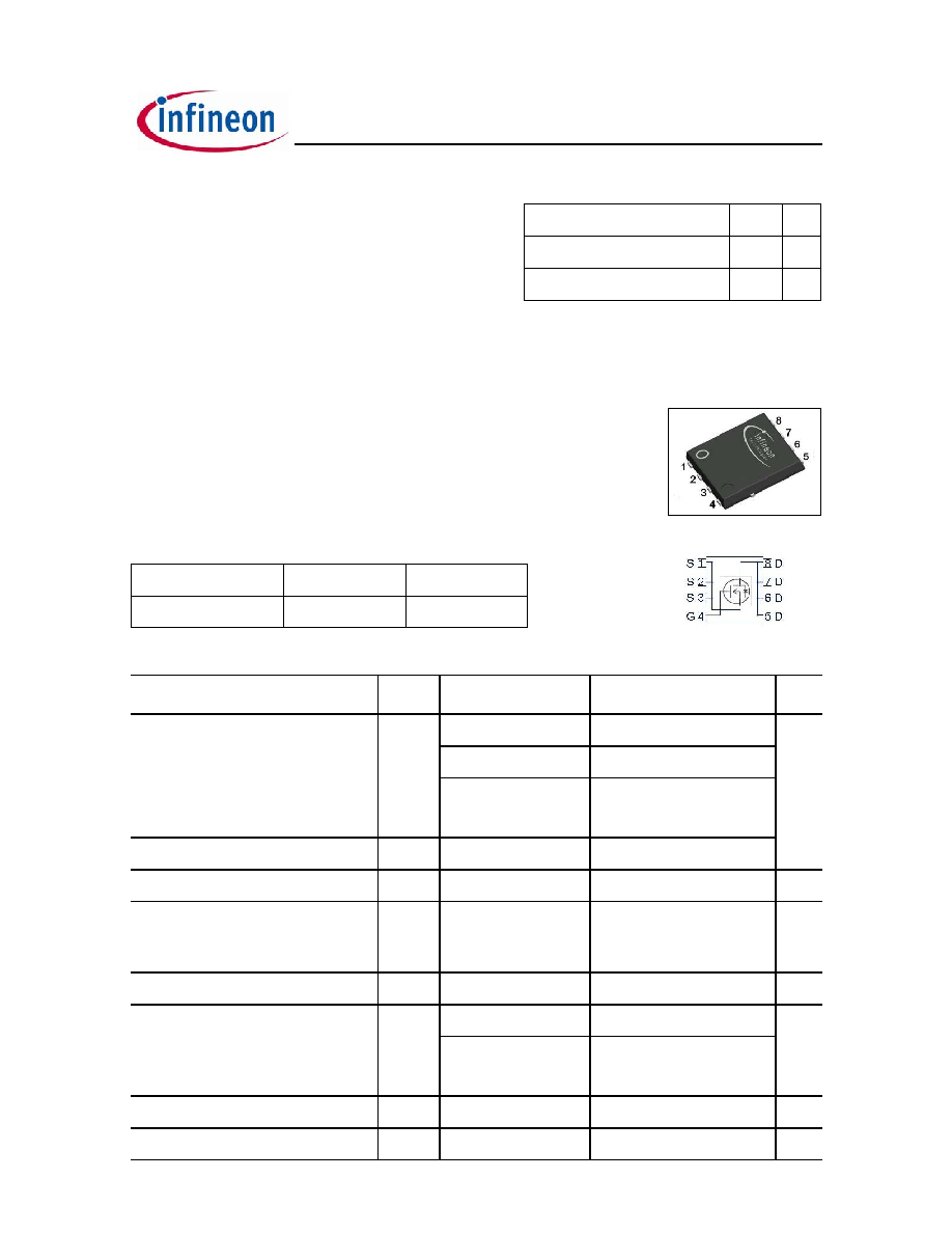
Product Summary
PG-TDSON-8
Type
Package
Marking
BSC027N03S
PG-TDSON-8
27N03S
Rev. 0.93
page 1
2006-05-09

BSC027N03S G
Parameter
Symbol Conditions
Unit
min.
typ.
max.
Thermal characteristics
Thermal resistance, junction - case
R
thJC
-
-
1.4
K/W
Thermal resistance,
R
thJA
minimal footprint
-
-
62
junction - ambient
6 cm
2
cooling area
2)
-
-
45
Electrical characteristics, at T
j
=25 įC, unless otherwise specified
Static characteristics
Drain-source breakdown voltage
V
(BR)DSS
V
GS
=0 V, I
D
=1 mA
30
-
-
V
Gate threshold voltage
V
GS(th)
V
DS
=V
GS
, I
D
=90 ĶA
1.2
1.6
2
Zero gate voltage drain current
I
DSS
V
DS
=30 V, V
GS
=0 V,
T
j
=25 įC
-
0.1
1
ĶA
V
DS
=30 V, V
GS
=0 V,
T
j
=125 įC
-
10
100
Gate-source leakage current
I
GSS
V
GS
=20 V, V
DS
=0 V
-
10
100
nA
Drain-source on-state resistance
R
DS(on)
V
GS
=4.5 V, I
D
=50 A
-
3.1
3.9
m
V
GS
=10 V, I
D
=50 A
-
2.3
2.7
Gate resistance
R
G
-
1.2
-
Transconductance
g
fs
|V
DS
|>2|I
D
|R
DS(on)max
,
I
D
=50 A
63
127
-
S
3)
See figure 3
1)
J-STD20 and JESD22
Values
2)
Device on 40 mm x 40 mm x 1.5 mm epoxy PCB FR4 with 6 cm
2
(one layer, 70 Ķm thick) copper area for drain
connection. PCB is vertical in still air.
Rev. 0.93
page 2
2006-05-09

BSC027N03S G
Parameter
Symbol Conditions
Unit
min.
typ.
max.
Dynamic characteristics
Input capacitance
C
iss
-
4920
6540
pF
Output capacitance
C
oss
-
1750
2330
Reverse transfer capacitance
C
rss
-
220
330
Turn-on delay time
t
d(on)
-
8.8
13
ns
Rise time
t
r
-
8
12
Turn-off delay time
t
d(off)
-
39
58
Fall time
t
f
-
6
10
Gate Charge Characteristics
4)
Gate to source charge
Q
gs
-
14
19
nC
Gate charge at threshold
Q
g(th)
-
7.9
10
Gate to drain charge
Q
gd
-
10
14
Switching charge
Q
sw
-
16
22
Gate charge total
Q
g
-
38
51
Gate plateau voltage
V
plateau
-
2.8
-
V
Gate charge total, sync. FET
Q
g(sync)
V
DS
=0.1 V,
V
GS
=0 to 5 V
-
33
44
nC
Output charge
Q
oss
V
DD
=15 V, V
GS
=0 V
-
39
52
Reverse Diode
Diode continous forward current
I
S
-
-
50
A
Diode pulse current
I
S,pulse
-
-
200
Diode forward voltage
V
SD
V
GS
=0 V, I
F
=50 A,
T
j
=25 įC
-
0.83
1
V
Reverse recovery charge
Q
rr
V
R
=15 V, I
F
=I
S
,
di
F
/dt =400 A/Ķs
-
-
18
nC
4)
See figure 16 for gate charge parameter definition
T
C
=25 įC
Values
V
GS
=0 V, V
DS
=15 V,
f =1 MHz
V
DD
=15 V, V
GS
=10 V,
I
D
=25 A, R
G
=2.7
V
DD
=15 V, I
D
=25 A,
V
GS
=0 to 5 V
Rev. 0.93
page 3
2006-05-09

BSC027N03S G
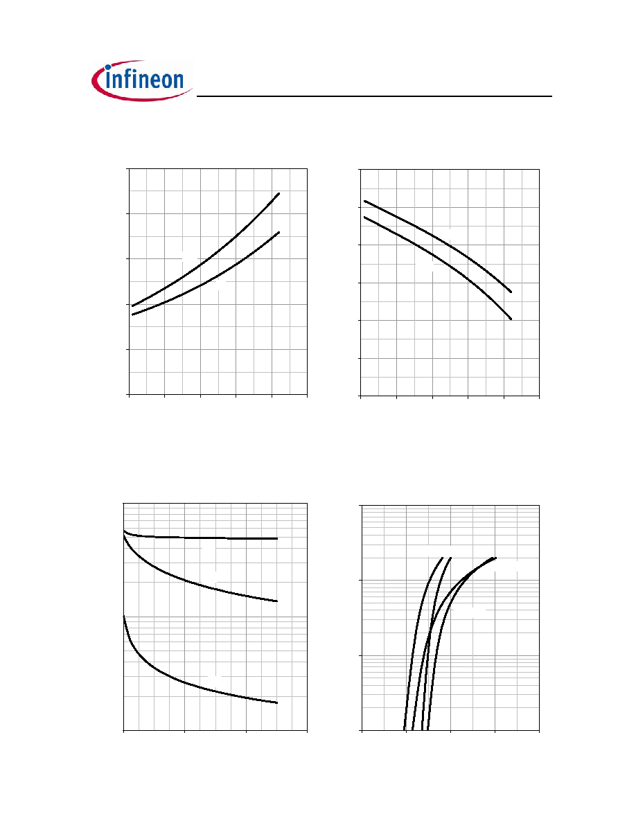
1 Power dissipation
2 Drain current
P
tot
=f(T
C
)
I
D
=f(T
C
); V
GS
10 V
3 Safe operating area
4 Max. transient thermal impedance
I
D
=f(V
DS
); T
C
=25 įC; D =0
Z
thJC
=f(t
p
)
parameter: t
p
parameter: D =t
p
/T
10 Ķs
100 Ķs
1 ms
10 ms
DC
10
3
10
2
10
1
10
0
10
2
10
1
10
0
10
-1
V
DS
[V]
I
D
[A]
limited by on-state
resistance
single pulse
0.01
0.02
0.05
0.1
0.2
0.5
10
0
10
-1
10
-2
10
-3
10
-4
10
-5
10
1
10
0
10
-1
10
-2
t
p
[s]
Z
thJ
C
[
K
/W]
0
20
40
60
80
100
0
40
80
120
160
T
C
[įC]
P
tot
[W]
0
20
40
60
80
100
120
0
40
80
120
160
T
C
[įC]
I
D
[A]
Rev. 0.93
page 4
2006-05-09

BSC027N03S G
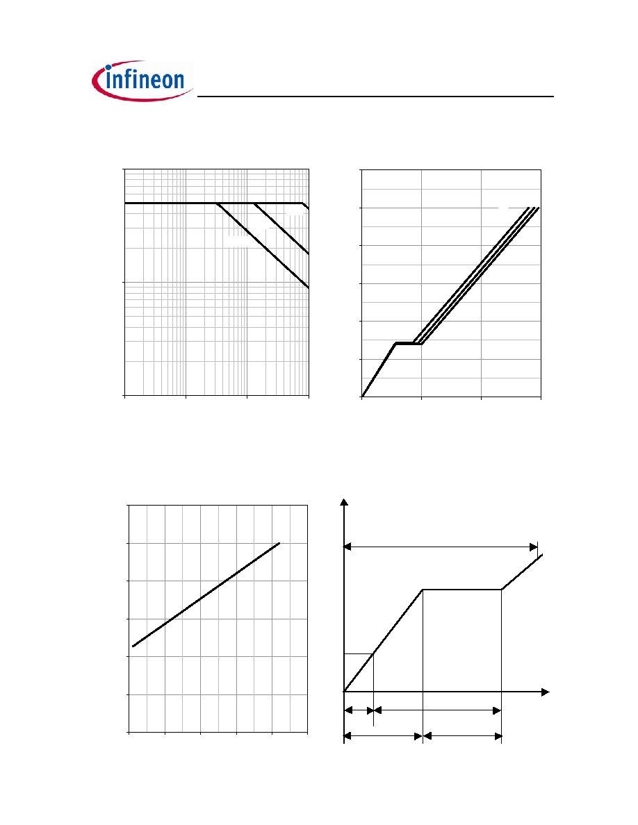
5 Typ. output characteristics
6 Typ. drain-source on resistance
I
D
=f(V
DS
); T
j
=25 įC
R
DS(on)
=f(I
D
); T
j
=25 įC
parameter: V
GS
parameter: V
GS
7 Typ. transfer characteristics
8 Typ. forward transconductance
I
D
=f(V
GS
); |V
DS
|>2|I
D
|R
DS(on)max
g
fs
=f(I
D
); T
j
=25 įC
parameter: T
j
3 V
3.2 V
3.4 V
3.7 V
4 V
4.5 V
10 V
0
2
4
6
8
10
0
50
100
I
D
[A]
R
DS
(on)
[m
]
25 įC
150 įC
0
40
80
120
160
200
0
1
2
3
4
5
V
GS
[V]
I
D
[A]
0
40
80
120
160
0
25
50
75
I
D
[A]
g
fs
[S]
2.8 V
3 V
3.2 V
3.4 V
3.7 V
4 V
4.5 V
10 V
0
40
80
120
160
200
0
1
2
3
V
DS
[V]
I
D
[A]
Rev. 0.93
page 5
2006-05-09
BSC027N03S G
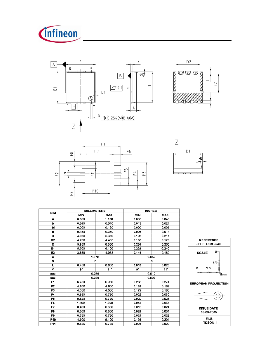
9 Drain-source on-state resistance
10 Typ. gate threshold voltage
R
DS(on)
=f(T
j
); I
D
=50 A; V
GS
=10 V
V
GS(th)
=f(T
j
); V
GS
=V
DS
parameter: I
D
11 Typ. capacitances
12 Forward characteristics of reverse diode
C =f(V
DS
); V
GS
=0 V; f =1 MHz
I
F
=f(V
SD
)
parameter: T
j
typ
98 %
0
1
2
3
4
5
-60
-10
40
90
140
190
T
j
[įC]
R
DS
(on)
[m
]
90 ĶA
900 ĶA
0
0.4
0.8
1.2
1.6
2
2.4
-60
-10
40
90
140
190
T
j
[įC]
V
G
S
(th)
[V]
Ciss
Coss
Crss
10
4
10
3
10
2
100
1000
10000
0
10
20
30
V
DS
[V]
C
[pF]
25 įC
150 įC
25 įC, 98%
150 įC, 98%
10
3
10
2
10
1
10
0
0
0.5
1
1.5
2
V
SD
[V]
I
F
[A]
Rev. 0.93
page 6
2006-05-09
BSC027N03S G
13 Avalanche characteristics
14 Typ. gate charge
I
AS
=f(t
AV
); R
GS
=25
V
GS
=f(Q
gate
); I
D
=25 A pulsed
parameter: T
j(start)
parameter: V
DD
15 Drain-source breakdown voltage
16 Gate charge waveforms
V
BR(DSS)
=f(T
j
); I
D
=1 mA
6 V
15 V
24 V
0
2
4
6
8
10
12
0
25
50
75
Q
gate
[nC]
V
GS
[V]
20
23
26
29
32
35
38
-60
-10
40
90
140
190
T
j
[įC]
V
BR(DS
S
)
[V]
V
GS
Q
gate
V
g s(th)
Q
g(th)
Q
g s
Q
g d
Q
sw
Q
g
25 įC
100 įC
125 įC
1
10
100
1
10
100
1000
t
AV
[Ķs]
I
AV
[A]
Rev. 0.93
page 7
2006-05-09
BSC027N03S G
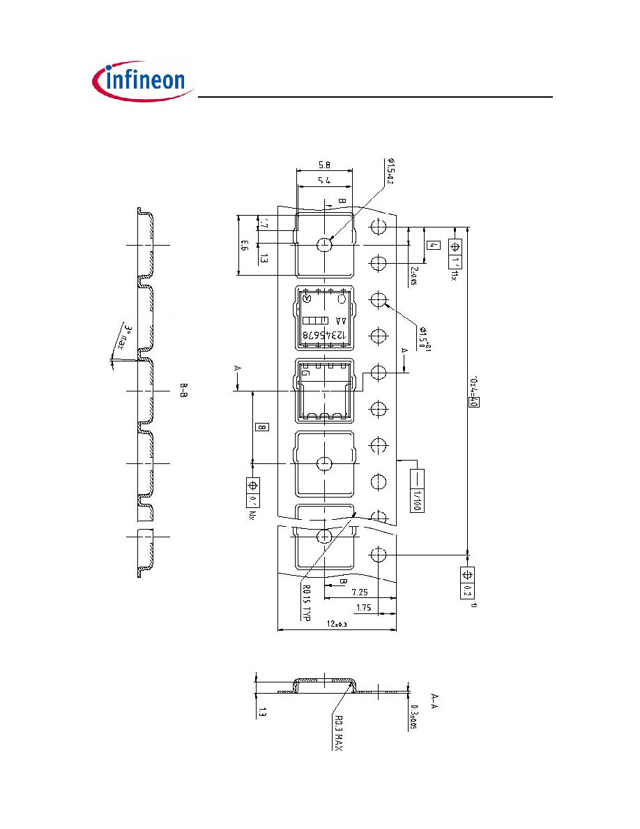
Package Outline
PG-TDSON-8
P-TDSON-8: Outline
Footprint
Dimensions in mm
Rev. 0.93
page 8
2006-05-09
BSC027N03S G
Package Outline
P-TDSON-8: Tape
Dimensions in mm
Rev. 0.93
page 9
2006-05-09

BSC027N03S G
Published by
Infineon Technologies AG
81726 MŁnchen, Germany
© Infineon Technologies AG 2006.
All Rights Reserved.
Attention please!
The information given in this data sheet shall in no event be regarded as a guarantee of conditions or
characteristics ("Beschaffenheitsgarantie"). With respect to any examples or hints given herein, any typical values
stated herein and/or any information regarding the application of the device, Infineon Technologies hereby
disclaims any and all warranties and liabilities of any kind, including without limitation warranties of
non-infringement of intellectual property rights of any third party.
Information
For further information on technology, delivery terms and conditions and prices please contact your nearest
Infineon Technologies Office (www.infineon.com ).
Warnings
Due to technical requirements components may contain dangerous substances. For information on the types in
question please contact your nearest Infineon Technologies Office.
Infineon Technologies Components may only be used in life-support devices or systems with the express written
approval of Infineon Technologies, if a failure of such components can reasonably be expected to cause the failure
of that life-support device or system, or to affect the safety or effectiveness of that device or system. Life support
devices or systems are intended to be implanted in the human body, or to support and/or maintain and sustain
sustain and/or protect human life. If they fail, it is reasonable to assume that the health of the user or other
persons may be endangered.
Rev. 0.93
page 10
2006-05-09