Semiconductor Group
1
Sep-12-1996
BSP 298
SIPMOS
Æ
Small-Signal Transistor
∑ N channel
∑ Enhancement mode
∑ Avalanche rated
∑ V
GS(th)
= 2.1 ... 4.0 V
Pin 1
Pin 2
Pin 3
Pin 4
G
D
S
D
Type
V
DS
I
D
R
DS(on)
Package
Marking
BSP 298
400 V
0.5 A
3
SOT-223
BSP 298
Type
Ordering Code
Tape and Reel Information
BSP 298
Q67000-S200
E6327
Maximum Ratings
Parameter
Symbol
Values
Unit
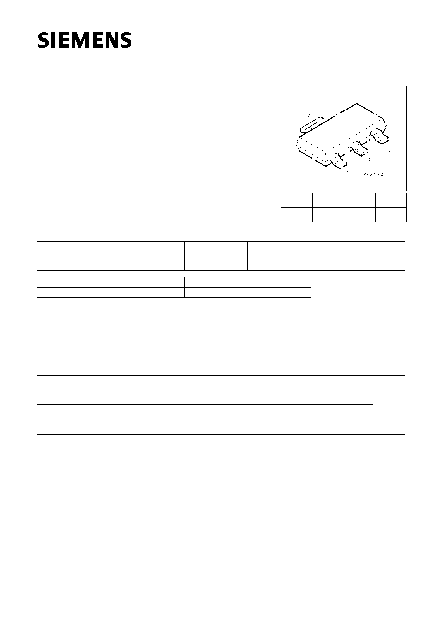
Continuous drain current
T
A
= 26 ∞C
I
D
0.5
A
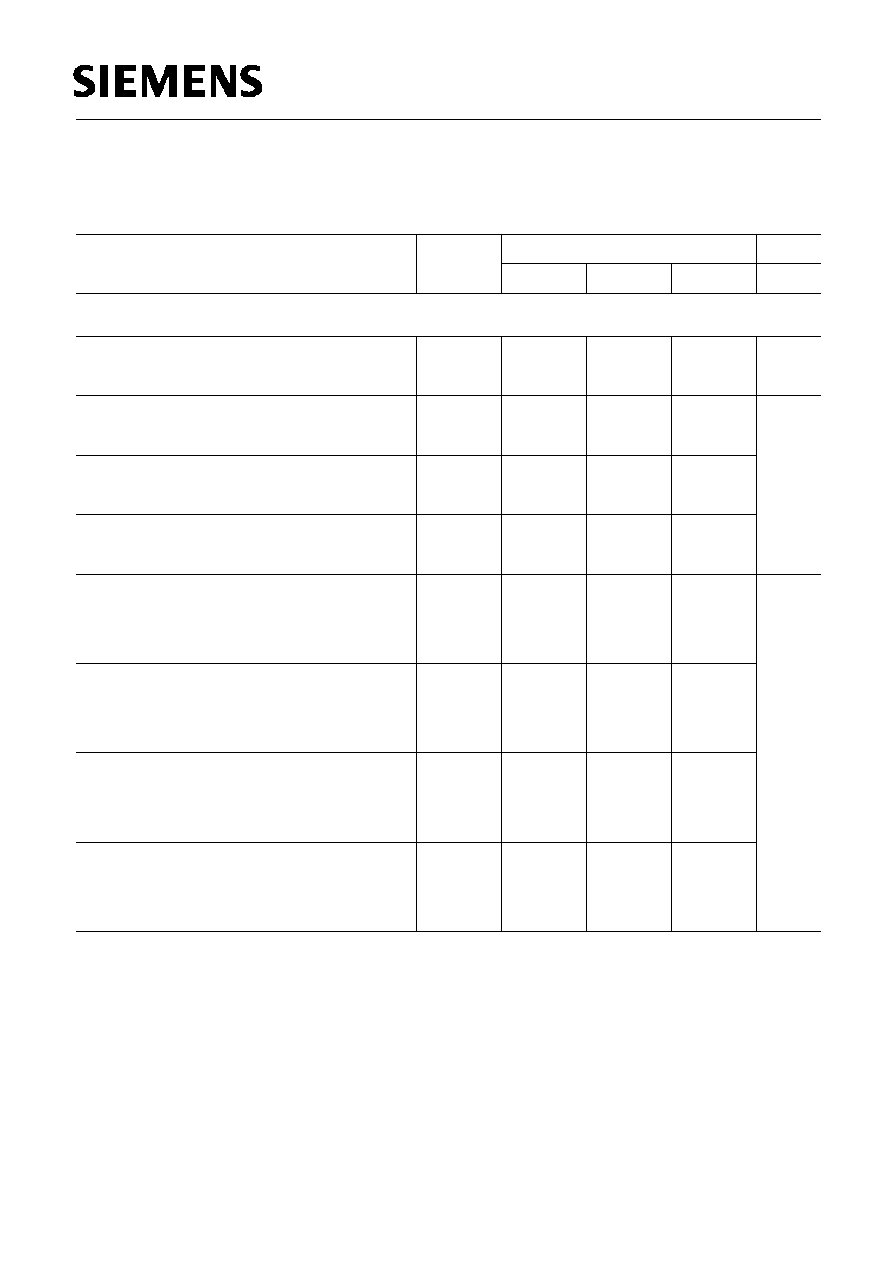
DC drain current, pulsed
T
A
= 25 ∞C
I
Dpuls
2
Avalanche energy, single pulse
I
D
= 1.35 A, V
DD
= 50 V, R
GS
= 25
L = 125 mH, T
j
= 25 ∞C
E
AS
130
mJ
Gate source voltage
V
GS
±
20
V
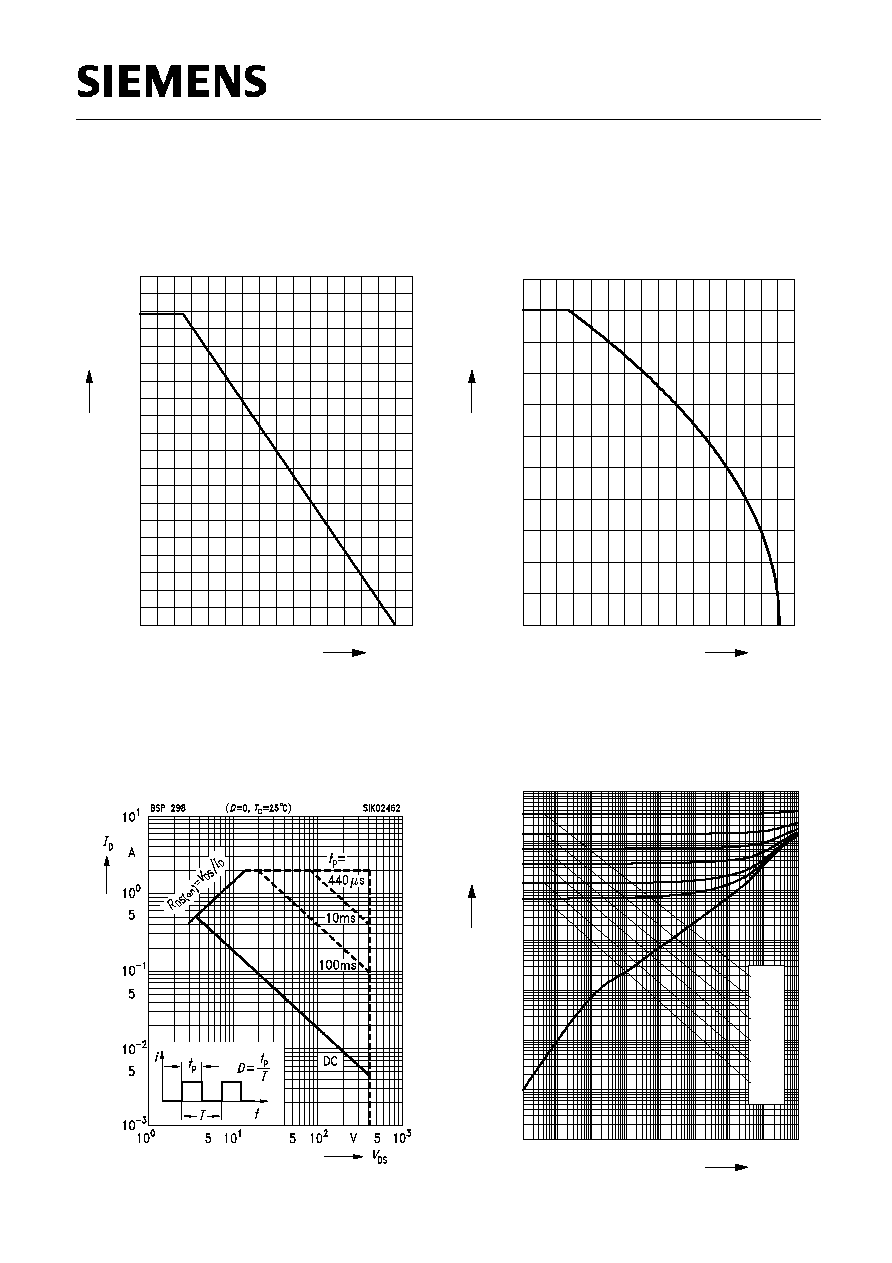
Power dissipation
T
A
= 25 ∞C
P
tot
1.8
W

Semiconductor Group
2
Sep-12-1996
BSP 298
Maximum Ratings
Parameter
Symbol
Values
Unit
Chip or operating temperature
T
j
-55 ... + 150
∞C
Storage temperature
T
stg
-55 ... + 150
Thermal resistance, chip to ambient air
R
thJA
70
K/W
Therminal resistance, junction-soldering point
1)
R
thJS
10
DIN humidity category, DIN 40 040
E
IEC climatic category, DIN IEC 68-1
55 / 150 / 56
1) Transistor on epoxy pcb 40 mm x 40 mm x 1,5 mm with 6 cm
2
copper area for drain connection
Electrical Characteristics,
at T
j
= 25∞C, unless otherwise specified
Parameter
Symbol
Values
Unit
min.
typ.
max.
Static Characteristics
Drain- source breakdown voltage
V
GS
= 0 V, I
D
= 0.25 mA, T
j
= 0 ∞C
V
(BR)DSS
400
-
-
V
Gate threshold voltage
V
GS=
V
DS,
I
D
= 1 mA
V
GS(th)
2.1
3
4
Zero gate voltage drain current
V
DS
= 400 V, V
GS
= 0 V, T
j
= 25 ∞C
V
DS
= 400 V, V
GS
= 0 V, T
j
= 125 ∞C
I
DSS
-
-
10
0.1
100
1
µA
Gate-source leakage current
V
GS
= 20 V, V
DS
= 0 V
I
GSS
-
10
100
nA
Drain-Source on-state resistance
V
GS
= 10 V, I
D
= 0.5 A
R
DS(on)
-
2.2
3
Semiconductor Group
3
Sep-12-1996
BSP 298
Electrical Characteristics,
at T
j
= 25∞C, unless otherwise specified
Parameter
Symbol
Values
Unit
min.
typ.
max.
Dynamic Characteristics
Transconductance
V
DS
2
*
I
D *
R
DS(on)max,
I
D
= 0.5 A
g
fs
0.5
1.2
-
S
Input capacitance
V
GS
= 0 V, V
DS
= 25 V, f = 1 MHz
C
iss
-
300
400
pF
Output capacitance
V
GS
= 0 V, V
DS
= 25 V, f = 1 MHz
C
oss
-
50
75
Reverse transfer capacitance
V
GS
= 0 V, V
DS
= 25 V, f = 1 MHz
C
rss
-
20
30
Turn-on delay time
V
DD
= 30 V, V
GS
= 10 V, I
D
= 0.3 A
R
GS
= 50
t
d(on)
-
10
15
ns
Rise time
V
DD
= 30 V, V
GS
= 10 V, I
D
= 0.3 A
R
GS
= 50
t
r
-
25
40
Turn-off delay time
V
DD
= 30 V, V
GS
= 10 V, I
D
= 0.3 A
R
GS
= 50
t
d(off)
-
30
40
Fall time
V
DD
= 30 V, V
GS
= 10 V, I
D
= 0.3 A
R
GS
= 50
t
f
-
20
30
Semiconductor Group
4
Sep-12-1996
BSP 298
Electrical Characteristics,
at T
j
= 25∞C, unless otherwise specified
Parameter
Symbol
Values
Unit
min.
typ.
max.
Reverse Diode
Inverse diode continuous forward current
T
A
= 25 ∞C
I
S
-
-
0.5
A
Inverse diode direct current,pulsed
T
A
= 25 ∞C
I
SM
-
-
2
Inverse diode forward voltage
V
GS
= 0 V, I
F
= 1 A, T
j
= 25 ∞C
V
SD
-
0.95
1.2
V
Reverse recovery time
V
R
= 100 V, I
F=
l
S,
di
F
/dt = 100 A/µs
t
rr
-
300
-
ns
Reverse recovery charge
V
R
= 100 V, I
F=
l
S,
di
F
/dt = 100 A/µs
Q
rr
-
2.5
-
µC