 | –≠–Ľ–Ķ–ļ—ā—Ä–ĺ–Ĺ–Ĺ—č–Ļ –ļ–ĺ–ľ–Ņ–ĺ–Ĺ–Ķ–Ĺ—ā: BSP350 | –°–ļ–į—á–į—ā—Ć:  PDF PDF  ZIP ZIP |

Mini PROFETģ BSP 350
Semiconductor Group
Page 1 of 6
08.04.97
MiniPROFET
∑
High-side switch
∑
Short-circuit protection
∑
Overtemperature protection with hysteresis
∑
Overload protection
∑
Overvoltage protection
∑
Reverse battery protection
1
)
∑
Switching inductive load
∑
Clamp of negative output voltage with inductive loads
∑
Maximum current internally limited
Package: SOT 223
Type
Ordering code
BSP 350
Q67000-S227
Maximum Ratings
Parameter
Symbol Values
Unit
Supply voltage
V
bb
50
V
Load current
self-limited
I
L
I
L(SC)
A
Maximum current through input pin (DC)
see internal circuit diagram
I
IN
Ī
15
mA
Inductive load switch-off energy dissipation
E
AS
5
mJ
Operating temperature range
Storage temperature range
T
j
T
stg
-40 ...+150
-55 ...+150
įC
Max. power dissipation (DC)
2)
T
A
= 25 įC
P
tot
1.7
W
Thermal resistance
chip - soldering point:
chip - ambient:
2
)
R
thJS
R
thJA
17
72
K/W
+ Vbb
GND
Control
Circuit
R
Temperature
Sensor
1
3
OUT
IN
RL
IN
2/4
1
) For 12 V applications only. Reverse load current only limited by connected load.
2
)
BSP 350 on epoxy pcb 40 mm x 40 mm x 1.5 mm with 6 cm2 copper area for Vbb connection
1
2
3
4
Pins:
1
2
3
4
IN
V
bb
OUT
V
bb

BSP 350
Semiconductor Group
Page 2
08.04.97
Electrical Characteristics
Parameter and Conditions
Symbol
Values
Unit
at
T
j
= 25 įC,
V
bb = 13.5V unless otherwise specified
min
typ
max
Load Switching Capabilities and Characteristics
On-state resistance (pin 2 to 3)
I
L
= 0.07 A, pin 1 = GND
T
j
= 25įC
T
j
= 150įC
V
bb
= 6 V, T
j
= 25įC
R
ON
--
--
--
4
8
5
5
10
10
Nominal load current (pin 2 to 3)
ISO Standard:
V
ON
= V
bb
-
V
OUT
= 0.5 V
T
S
= 85 įC
I
L(ISO)
0.07
--
--
A
Turn-on time
to 90%
V
OUT
Turn-off time
to 10%
V
OUT
R
L
= 270
t
on
t
off
--
--
60
70
100
140
Ķ
s
Slew rate on
10 to 30%
V
OUT
,
R
L
= 270
d
V /dt
on
--
4
6
V/
Ķ
s
Slew rate off
70 to 40%
V
OUT
,
R
L
= 270
-d
V/dt
off
--
2
6
Input
OFF state input current
T
j
= - 40...+150įC
R
L
= 270
,
V
OUT
0,1V
I
IN(off)
--
--
0.05
mA
ON state input current, (pin 1 grounded)
3
)
T
j
= - 40...+150įC
I
IN(on)
--
0.3
1
mA
Operating Parameters
Operating voltage (pin 1 grounded)
4
)
T
j
= - 40...+150įC
V
bb(on)
4.9
--
45
V
Leakage current (pin 2 to 3, pin 1 open)
T
j
= 25įC
T
j
=150įC
I
bb(off)
--
--
1
1.2
10
10
Ķ
A
3
) Driver circuit must be capable to drive currents
>
1mA.
4
) Below Vbb=4.5 V typ. without chargepump, Vout
Vbb - 2 V
BSP 350
Semiconductor Group
Page 3
08.04.97
Parameter and Conditions
Symbol
Values
Unit
at
T
j
= 25 įC,
V
bb = 13.5V unless otherwise specified
min
typ
max
Protection Functions
Current limit (pin 2 to 3)
5
)
T
j
= 25įC
T
j
= -40...+150į
I
L(SC)
0.2
0.1
0.5
--
1
1.2
A
Thermal overload trip temperature
T
jt
150
--
--
įC
Thermal hysteresis
T
jt
--
20
--
K
Overvoltage protection
T
j
=-40...+150įC
V
bbin(AZ)
50
56
--
V
Output clamp (ind. load switch off)
at
V
OUT
=
V
bb
-
V
ON(CL)
V
ON(CL)
--
56
--
V
Inductive load switch-off energy dissipation
6
)
E
AS
--
--
5
mJ
Reverse battery resistor (pin 1 to 2)
R
IN
--
1
--
k
Reverse Diode
Continious reverse drain current
T
j
= 25įC
I
S
--
--
0.2
A
Pulsed reverse drain current
T
j
= 25įC
I
SM
--
--
0.8
A
Diode forward on voltage
I
F
= 0.2 A, I
IN
=
0.05 mA
V
SD
--
0.9
1.2
V
5
)
load current limits onset at IL * Ron approx. 1V
short circuit protection: combination of current limit and thermal overload switch off
6
)
while demagnetizing load inductance, dissipated energy is
E
AS=
(VON(CL) * iL(t) dt,
approx.
E
AS=
1
/
2
* L * I
2
L
* (
V
ON(CL)
V
ON(CL)
-V
bb
)
BSP 350
Semiconductor Group
Page 4
08.04.97
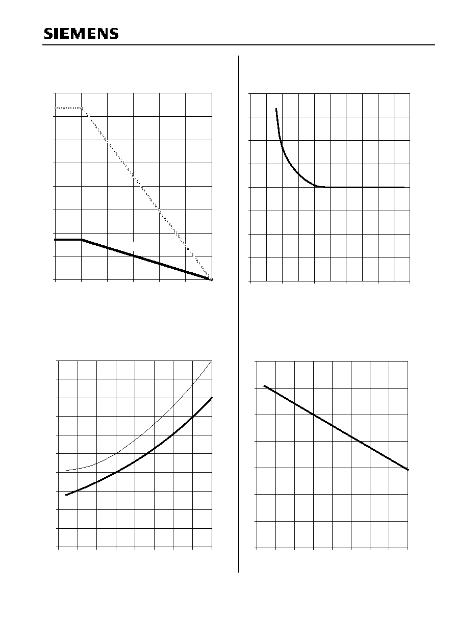
Max allowable power dissipation
Ptot = f (TA,TSP)
Ptot [W]
0
1
2
3
4
5
6
7
8
0
25
50
75
100
125
150
T
A
SP
T
TA, TSP[įC]
On state resistance (Vbb- pin to OUT pin)
RON = f (Tj);Vbb = 13.5 V;IL = 70 mA
RON [
]
0
1
2
3
4
5
6
7
8
9
10
-50
-25
0
25
50
75
100 125 150
typ
98%
TJ [įC]
Typ. on state resistance (Vbb- pin to OUT pin)
RON = f (Vbb); IL = 70 mA; Tj = 25įC
RON [
]
0
1
2
3
4
5
6
7
8
0
5
10
15
20
25
Vbb [V]
Typ. short circuit current
IL(SC) = f(Tj); Vbb = 13.5V
ILSC [
]
0
0.1
0.2
0.3
0.4
0.5
0.6
0.7
-50
-25
0
25
50
75
100 125 150
TJ [įC]
BSP 350
Semiconductor Group
Page 5
08.04.97
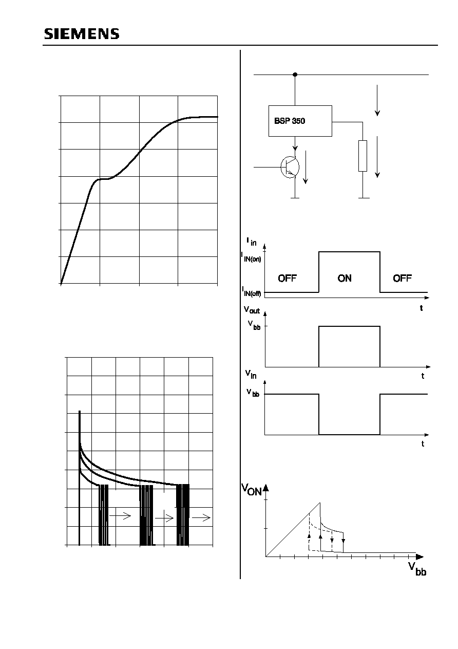
Typ. short circuit current
IL(SC) = f(VON); Vbb = 13.5V; Tj = 25įC
ILSC [
]
0
0.1
0.2
0.3
0.4
0.5
0.6
0.7
0
2
4
6
8
VON [V]
Typ. short circuit current
IL(SC) = f(t); Vbb = 13.5V
no heatsink; Parameter: TjStart
IL(SC)[mA]
0
200
400
600
800
1000
-0,5
0,5
1,5
2,5
3,5
4,5
5,5
-40įC
25įC
125įC
t[s]
Test circuit
V
Vin
Vbb
Iin
2/4
1
3
out
Von
Turn on conditions
Chargepump threshold
VON = f (Vbb)
typ.
max.
2
4
6
8
2
4
BSP 350
Semiconductor Group
Page 6
08.04.97
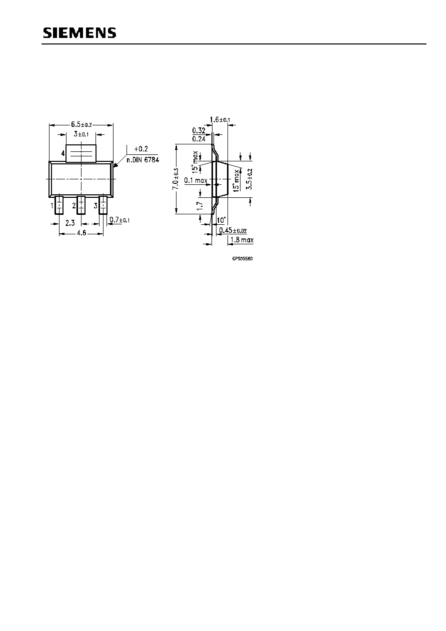
Package:
all dimensions in mm.
SOT 223/3:
Edition 7.97
Published by Siemens AG,
Bereich Halbleiter Vetrieb,
Werbung, BalanstraŖe 73,
81541 MŁnchen
© Siemens AG 1997
All Rights Reserved.
Attention please!
As far as patents or other rights of third parties are concerned, liability is only assumed for components, not for
applications, processes and circuits implemented within components or assemblies.
The information describes a type of component and shall not be considered as warranted characteristics.
Terms of delivery and rights to change design reserved.
For questions on technology, delivery and prices please contact the Semiconductor Group Offices in Germany or
the Siemens Companies and Representatives worldwide (see address list).
Due to technical requirements components may contain dangerous substances. For information on the types in
question please contact your nearest Siemens Office, Semiconductor Group.
Siemens AG is an approved CECC manufacturer.
Packing
Please use the recycling operators known to you. We can also help you - get in touch with your nearest sales office.
By agreement we will take packing material back, if it is sorted. You must bear the costs of transport.
For packing material that is returned to us unsorted or which we are not obliged to accept, we shall have to invoice
you for any costs incurred.
Components used in life-support devices or systems must be expressly authorized for such purpose!
Critical components
1
of the Semiconductor Group of Siemens AG, may only be used in life-support devices or
systems
2
with the express written approval of the Semiconductor Group of Siemens AG.
1) A critical component is a component used in a life-support device or system whose failure can reasonably be
expected to cause the failure of that life-support device or system, or to affect its safety or effectiveness of that
device or system.
2) Life support devices or systems are intended (a) to be implanted in the human body, or (b) to support and/or
maintain and sustain and/or protecf human life. If they fail, it is reasonable to assume that the health of the user or
other persons may be endangered.