 | –≠–Ľ–Ķ–ļ—ā—Ä–ĺ–Ĺ–Ĺ—č–Ļ –ļ–ĺ–ľ–Ņ–ĺ–Ĺ–Ķ–Ĺ—ā: BSS138N | –°–ļ–į—á–į—ā—Ć:  PDF PDF  ZIP ZIP |

BSS138N
SIPMOS
ģ
Small-Signal-Transistor
Features
∑ N-channel
∑ Enhancement mode
∑ Logic level
∑ dv /dt rated
Maximum ratings, at T
j
=25 įC, unless otherwise specified
Parameter
Symbol Conditions
Unit
Continuous drain current
I
D
T
A
=25 įC
0.23
A
T
A
=70 įC
0.18
Pulsed drain current
I
D,pulse
T
A
=25 įC
0.92
Reverse diode dv /dt
dv /dt
I
D
=0.23 A, V
DS
=48 V,
di /dt =200 A/Ķs,
T
j,max
=150 įC
6
kV/Ķs
Gate source voltage
V
GS
Ī20
V
ESD sensitivity (HBM) as per
MIL-STD 883
Class 1
Power dissipation
P
tot
T
A
=25 įC
0.36
W
Operating and storage temperature
T
j
, T
stg
-55 ... 150
įC
IEC climatic category; DIN IEC 68-1
55/150/56
Value
V
DS
60
V
R
DS(on),max
3.5
I
D
0.23
A
Product Summary
SOT-23
Type
Package
Ordering Code
Tape and Reel Information
Marking
BSS138N
SOT-23
Q67042-S4184
E6327: 3000 pcs/reel
SKs
BSS138N
SOT-23
Q67042-S4190
E6433: 10000 pcs/reel
SKs
Rev. 2.1
page 1
2004-04-15

BSS138N
Parameter
Symbol Conditions
Unit
min.
typ.
max.
Thermal characteristics
Thermal resistance,
junction - minimal footprint
R
thJA
-
-
350
K/W
Electrical characteristics, at T
j
=25 įC, unless otherwise specified
Static characteristics
Drain-source breakdown voltage
V
(BR)DSS
V
GS
= 0 V, I
D
=250 ĶA
60
-
-
V
Gate threshold voltage
V
GS(th)
V
GS
=V
DS
, I
D
=26 ĶA
0.6
1.0
1.4
Drain-source leakage current
I
D (off)
V
DS
=60 V,
V
GS
=0 V, T
j
=25 įC
-
-
0.1
ĶA
V
DS
=60 V,
V
GS
=0 V, T
j
=150 įC
-
10
100
Gate-source leakage current
I
GSS
V
GS
=20 V, V
DS
=0 V
-
1
10
nA
Drain-source on-state resistance
R
DS(on)
V
GS
=4.5 V, I
D
=0.03 A
-
3.3
4.0
V
GS
=4.5 V, I
D
=0.19 A
-
3.5
6.0
V
GS
=10 V, I
D
=0.23 A
-
2.2
3.5
Transconductance
g
fs
|V
DS
|>2|I
D
|R
DS(on)max
,
I
D
=0.18 A
0.1
0.2
-
S
Values
Rev. 2.1
page 2
2004-04-15
BSS138N
Parameter
Symbol Conditions
Unit
min.
typ.
max.
Dynamic characteristics
Input capacitance
C
iss
-
32
43
pF
Output capacitance
C
oss
-
7.2
10
Reverse transfer capacitance
C
rss
-
2.8
4.2
Turn-on delay time
t
d(on)
-
2.3
3.5
ns
Rise time
t
r
-
3.0
4.5
Turn-off delay time
t
d(off)
-
6.7
10
Fall time
t
f
-
8.2
12
Gate Charge Characteristics
Gate to source charge
Q
gs
-
0.10
0.14
nC
Gate to drain charge
Q
gd
-
0.3
0.4
Gate charge total
Q
g
-
1.0
1.4
Gate plateau voltage
V
plateau
-
3.3
-
V
Reverse Diode
Diode continous forward current
I
S
-
-
0.23
A
Diode pulse current
I
S,pulse
-
-
0.92
Diode forward voltage
V
SD
V
GS
=0 V, I
F
=0.23 A,
T
j
=25 įC
-
0.83
1.2
V
Reverse recovery time
t
rr
-
9.1
14.5
ns
Reverse recovery charge
Q
rr
-
3.3
5
nC
V
R
=30 V, I
F
=0.23 A,
di
F
/dt =100 A/Ķs
T
A
=25 įC
Values
V
GS
=0 V, V
DS
=25 V,
f =1 MHz
V
DD
=30 V, V
GS
=10 V,
I
D
=0.23 A, R
G
=6
V
DD
=48 V, I
D
=0.23 A,
V
GS
=0 to 10 V
Rev. 2.1
page 3
2004-04-15
BSS138N
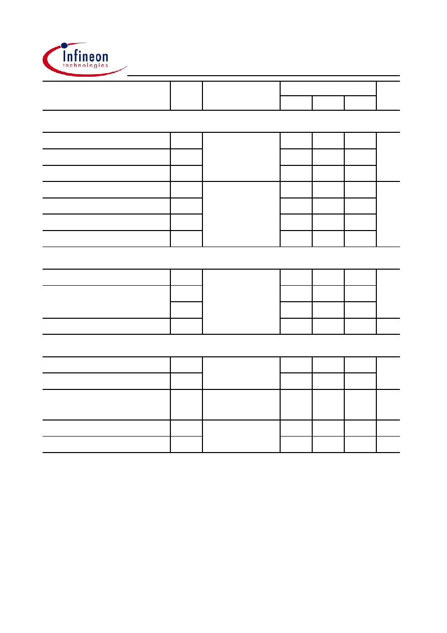
1 Power dissipation
2 Drain current
P
tot
=f(T
A
)
I
D
=f(T
A
); V
GS
10 V
3 Safe operation area
4 Max. transient thermal impedance
I
D
=f(V
DS
); T
A
=25 įC; D =0
Z
thJA
=f(t
p
)
parameter: t
p
parameter: D =t
p
/T
100 ms
10 Ķs
100 Ķs
1 ms
10 ms
DC
10
1
10
0
10
-1
10
-2
10
-3
1
10
100
V
DS
[V]
I
D
[A]
limited by on-state
resistance
single pulse
0.01
0.02
0.05
0.1
0.2
0.5
10
1
10
0
10
-1
10
-2
10
-3
10
-4
10
-5
10
3
10
2
10
1
10
0
t
p
[s]
Z
thJA
[K/W]
0
0.1
0.2
0.3
0.4
0
40
80
120
160
T
A
[įC]
P
tot
[W]
0
0.05
0.1
0.15
0.2
0.25
0
40
80
120
160
T
A
[įC]
I
D
[A]
Rev. 2.1
page 4
2004-04-15
BSS138N
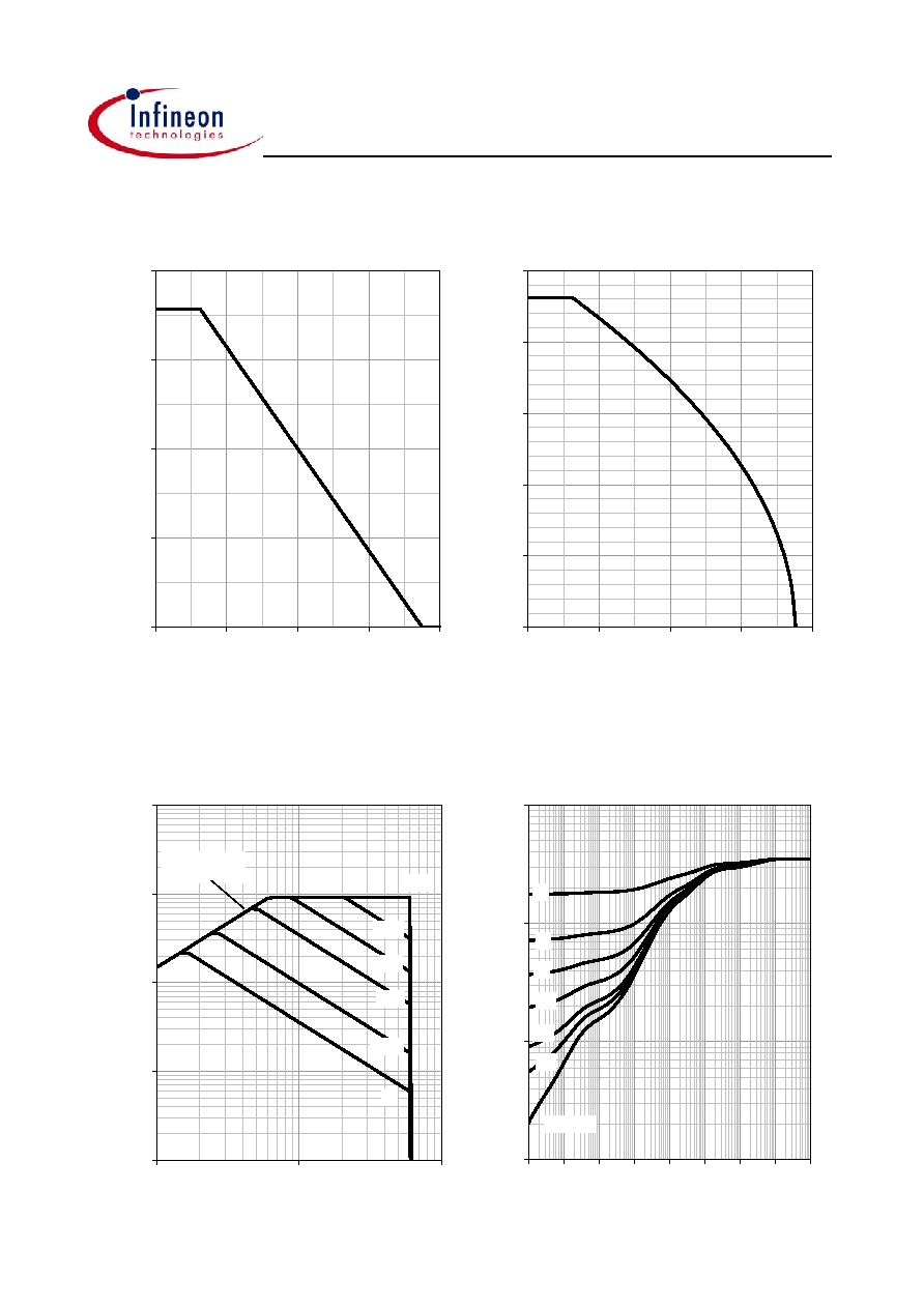
5 Typ. output characteristics
6 Typ. drain-source on resistance
I
D
=f(V
DS
); T
j
=25 įC
R
DS(on)
=f(I
D
); T
j
=25 įC
parameter: V
GS
parameter: V
GS
7 Typ. transfer characteristics
8 Typ. forward transconductance
I
D
=f(V
GS
); |V
DS
|>2|I
D
|R
DS(on)max
g
fs
=f(I
D
); T
j
=25 įC
2.9 V
3.2 V
3.5 V
4 V
4.5 V
5 V
7 V
10 V
0
2
4
6
8
10
0
0.1
0.2
0.3
0.4
0.5
I
D
[A]
R
D
S
(on)
[
]
0
0.1
0.2
0.3
0.4
0.5
0.6
0
1
2
3
4
5
V
GS
[V]
I
D
[A]
0
0.05
0.1
0.15
0.2
0.25
0.3
0.35
0.4
0.00
0.10
0.20
0.30
0.40
I
D
[A]
g
fs
[S]
2.9 V
3.2 V
3.5 V
4 V
4.5 V
5 V
7 V
10 V
0
0.1
0.2
0.3
0.4
0.5
0.6
0
1
2
3
4
5
V
DS
[V]
I
D
[A]
Rev. 2.1
page 5
2004-04-15