 | –≠–ª–µ–∫—Ç—Ä–æ–Ω–Ω—ã–π –∫–æ–º–ø–æ–Ω–µ–Ω—Ç: BTS129 | –°–∫–∞—á–∞—Ç—å:  PDF PDF  ZIP ZIP |
TEMPFET
Æ
BTS 129
1 19.02.04
3
2
1
Features
q
N channel
q
Enhancement mode
q
Temperature sensor with thyristor characteristic
q
The drain pin is electrically shorted to the tab
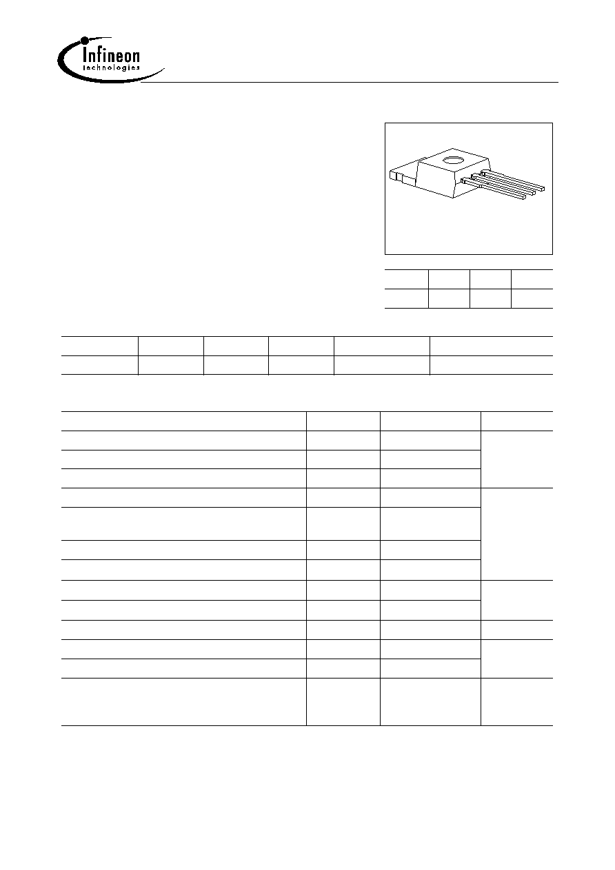
Pin
1
2
3
G
D
S
Type
V
DS
I
D
R
DS(on)
Package
Ordering Code
BTS 129
60 V
27 A
0.05
TO-220AB
C67078-A5013-A2
Maximum Ratings
Parameter
Symbol
Values
Unit
Drain-source voltage
V
DS
60
V
Drain-gate voltage,
R
GS
= 20 k
V
DGR
60
Gate-source peak voltage, aperiodic
V
gs
±
20
Continuous drain current,
T
C
= 25
∞
C
I
D
27
A
ISO drain current
T
C
= 85
∞
C,
V
GS
= 10 V,
V
DS
= 0.5 V
I
D-ISO
7.5
Pulsed drain current,
T
C
= 25
∞
C
I
D puls
108
Short circuit current,
T
j
= ≠ 55 ... + 150
∞
C
I
SC
80
Short circuit dissipation,
T
j
= ≠ 55 ... + 150
∞
C
P
SCmax
1200
W
Power dissipation
P
tot
75
Operating and storage temperature range
T
j
,
T
stg
≠ 55 ... + 150
∞
C
DIN humidity category, DIN 40 040
≠
E
≠
IEC climatic category, DIN IEC 68-1
≠
55/150/56
Thermal resistance
Chip-case
Chip-ambient
R
th JC
R
th JA
1.67
75
K/W

TEMPFET
Æ
BTS 129
2 19.02.04
Electrical Characteristics
at
T
j
= 25
∞
C, unless otherwise specified.
Parameter
Symbol
Values
Unit
min.
typ.
max.
Static Characteristics
Drain-source breakdown voltage
V
GS
= 0
, I
D
= 0.25 mA
V
(BR)DSS
60
≠
≠
V
Gate threshold voltage
V
GS
=
V
DS
, I
D
= 1 mA
V
GS(th)
2.5
3.0
3.5
Zero gate voltage drain current
V
GS
= 0 V,
V
DS
= 60 V
T
j
= 25
∞
C
T
j
= 150
∞
C
I
DSS
≠
≠
1
100
10
300
µ
A
Gate-source leakage current
V
GS
= 20 V,
V
DS
= 0
T
j
= 25
∞
C
T
j
= 150
∞
C
I
GSS
≠
≠
10
2
100
4
nA
µ
A
Drain-source on-state resistance
V
GS
= 10 V
, I
D
=17 A
R
DS(on)
≠
0.04
0.05
Dynamic Characteristics
Forward transconductance
V
DS
2
◊
I
D
◊
R
DS(on)max
,
I
D
= 17 A
g
fs
8.0
13.0
18.0
S
Input capacitance
V
GS
= 0
, V
DS
= 25 V,
f
= 1 MHz
C
iss
700
940
1250
pF
Output capacitance
V
GS
= 0
, V
DS
= 25 V,
f
= 1 MHz
C
oss
≠
500
750
Reverse transfer capacitance
V
GS
= 0
, V
DS
= 25 V,
f
= 1 MHz
C
rss
≠
180
270
Turn-on time
t
on
, (
t
on
=
t
d(on)
+
t
r
)
V
CC
= 30 V,
V
GS
= 10 V,
I
D
= 3 A,
R
GS
= 50
t
d(on)
≠
25
40
ns
t
r
≠
60
90
Turn-off time
t
off
, (
t
off
=
t
d(off)
+
t
f
)
V
CC
= 30 V,
V
GS
= 10 V,
I
D
= 3 A,
R
GS
= 50
t
d(off)
≠
100
130
t
f
≠
75
95

TEMPFET
Æ
BTS 129
3 19.02.04
Electrical Characteristics (cont'd)
at
T
j
= 25
∞
C, unless otherwise specified.
Parameter
Symbol
Values
Unit
min.
typ.
max.
Reverse Diode
Continuous source current
I
S
≠
≠
27
A
Pulsed source current
I
SM
≠
≠
108
Diode forward on-voltage
I
F
= 27 A,
V
GS
= 0 V
V
SD
≠ 1.3 1.8
V
Reverse recovery time
I
F
=
I
S
, d
i
F
/d
t
= 100 A/
µ
s,
V
R
= 30 V
t
rr
≠
150
≠
ns
Reverse recovery charge
I
F
=
I
S
, d
i
F
/d
t
= 100 A/
µ
s,
V
R
= 30 V
Q
rr
≠
1.0
≠
µ
C
Temperature Sensor
Forward voltage
I
TS(on)
= 10 mA,
T
j
= ≠ 55 ... + 150
∞
C
Sensor override,
t
p
100
µ
s
T
j
= ≠ 55 ... + 160
∞
C
V
TS(on)
0.7
≠
1.4
≠
1.5
10
V
Forward current
T
j
= ≠ 55 ... + 150
∞
C
Sensor override,
t
p
100
µ
s
T
j
= ≠ 55 ... + 160
∞
C
I
TS(on)
≠
≠
≠
≠
10
600
mA
Holding current,
V
TS(off)
= 5 V,
T
j
= 25
∞
C
T
j
= 150
∞
C
I
H
0.05
0.05
0.1
0.2
0.5
0.3
Switching temperature
V
TS
= 5 V
T
TS(on)
150
≠
≠
∞
C
Turn-off time
V
TS
= 5 V,
I
TS(on)
= 2 mA
t
off
0.5
≠
2.5
µ
s
TEMPFET
Æ
BTS 129
4 19.02.04
Examples for short-circuit protection
at
T
j
= ≠ 55 ... + 150
∞
C, unless otherwise specified.
Parameter
Symbol
Examples
Unit
1
2
≠
Drain-source voltage
V
DS
15
30
≠
V
Gate-source voltage
V
GS
8.1
5.9
≠
Short-circuit current
I
SC
80
37
≠
A
Short-circuit dissipation
P
SC
1200
1100
≠
W
Response time
T
j
= 25
∞
C, before short circuit
t
SC(off)
25
25
≠
ms
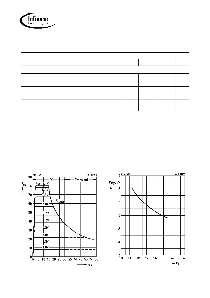
Short-circuit protection
I
SC
=
f
(
V
DS
)
Parameter
: V
GS
Diagram to determine
I
SC
for
T
j
= ≠ 55 ... + 150
∞
C
Max. gate voltage
V
GS(SC)
=
f
(
V
DS
)
Parameter:
T
j
= ≠ 55 ... + 150
∞
C

TEMPFET
Æ
BTS 129
5 19.02.04
Typical output characteristics
I
D
=
f
(
V
DS
)
Parameter
: t
p
= 80
µ
s
Typ. drain-source on-state resistance
R
DS(on)
=
f
(
I
D
)
Parameter
: V
GS
SIT00562
0
20
P
tot
D
BTS 129
A
1
2
3
4
5
V
0
10
30
40
50
= 75W
V
GS
= 20V
9V
8V
7.5V
6.5V
6V
5.5V
5V
4.5V
4V
DS
V
60
10V
7V
Safe operating area
I
D
=
f
(
V
DS
)
Parameter:
D
= 0.01,
T
C
= 25
∞
C
Drain-source on-state resistance
R
DS(on)
=
f
(
T
j
)
Parameter:
I
D
= 17 A,
V
GS
= 10 V (spread)
TEMPFET
Æ
BTS 129
6 19.02.04
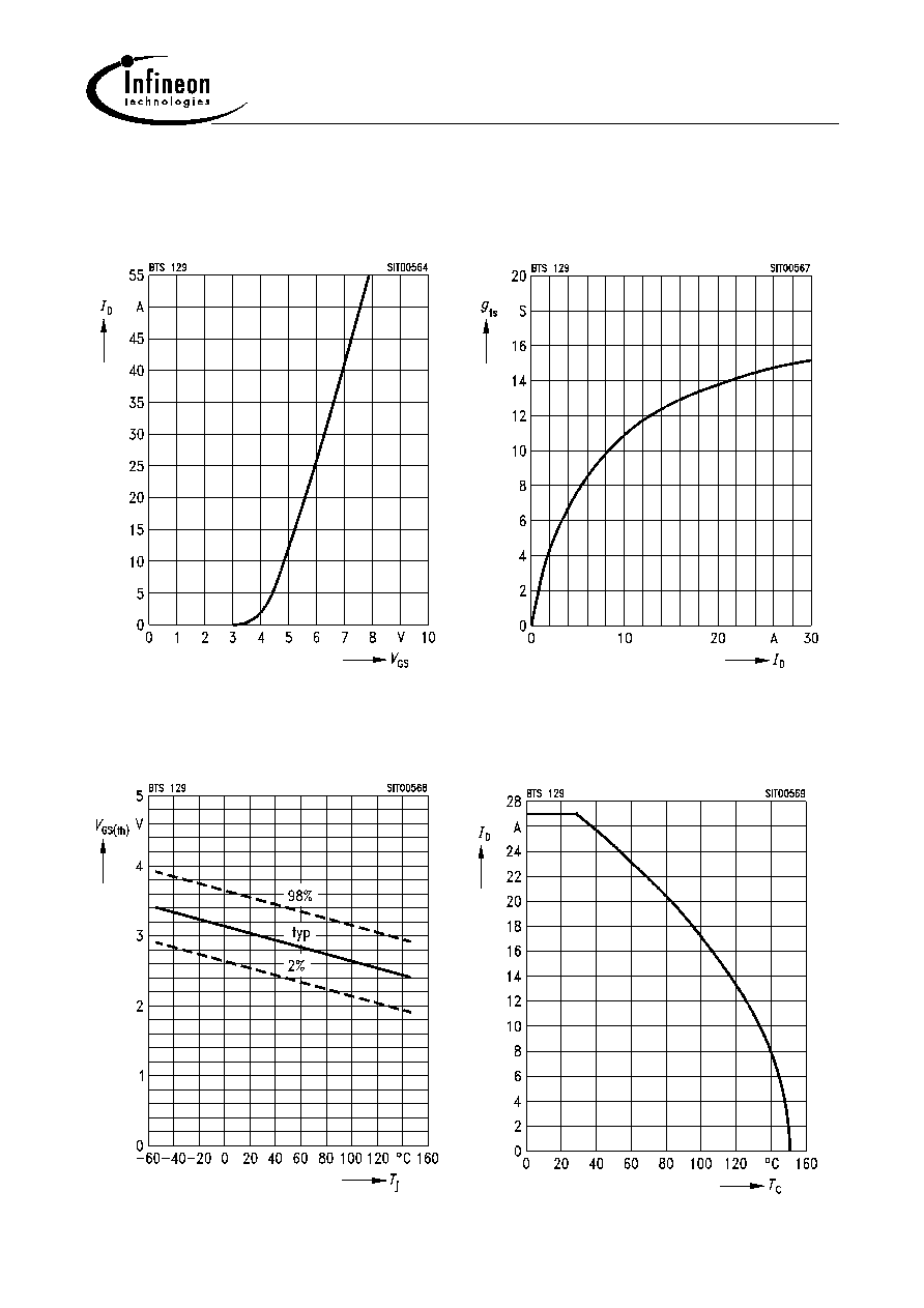
Typ. transfer characteristic
I
D
=
f
(
V
GS
)
Parameter
: t
p
= 80
µ
s,
V
DS
= 25 V
Gate threshold voltage
V
GS(th)
=
f
(
T
j
)
Parameter
: V
DS
=
V
GS
,
I
D
= 1 mA
Typ. transconductance
g
fs
=
f
(
I
D
)
Parameter:
t
p
= 80
µ
s,
V
DS
= 25 V
Continuous drain current
I
D
=
f
(
T
C
)
Parameter:
V
GS
10 V

TEMPFET
Æ
BTS 129
7 19.02.04
Typ. gate-source leakage current
I
GSS
=
f
(
T
C
)
Parameter:
V
GS
= 20 V,
V
DS
= 0
Forward characteristics of reverse diode
I
F
=
f
(
V
SD
)
Parameter
: T
j
,
t
p
= 80
µ
s
Typ. capacitances
C
=
f
(
V
DS
)
Parameter:
V
GS
= 0,
f
= 1 MHz
Transient thermal impedance
Z
thJC
=
f
(
t
p
)
Parameter
: D
=
t
p
/
T
TEMPFET
Æ
BTS 129
8 19.02.04
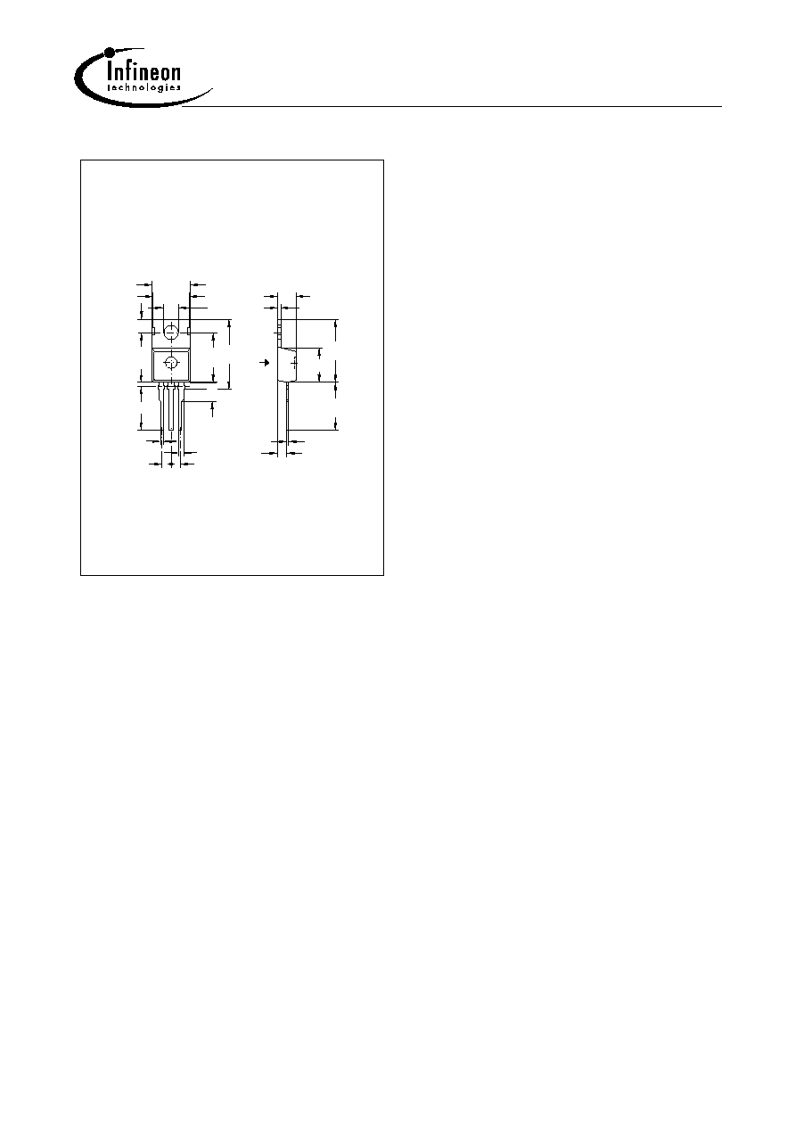
TO 220 AB
Ordering Code
Standard
C67078-A5013-A2
3.7
9.5
9.9
4.6
0.75
1.05
2.54
2.54
17.5
2.8
12.8
0.5
2.4
13.5
9.2
15.6
1.3
4.4
GPT05155
1)
3) max. 14.5 by dip tinning press burr max. 0.05
2) dip tinning
1) punch direction, burr max. 0.04
3)
2)
1

TEMPFET
Æ
BTS 129
9 19.02.04
Edition 04.97
Published by Infineon Technologies AG,
St.-Martin-Strasse 53,
D-81541 M¸nchen, Germany
©
Infineon Technologies AG 2000.
All Rights Reserved.
Attention please!
The information herein is given to describe certain components and shall not be considered as warranted
characteristics.
Terms of delivery and rights to technical change reserved.
We hereby disclaim any and all warranties, including but not limited to warranties of non-infringement, regarding
circuits, descriptions and charts stated herein.
Infineon Technologies is an approved CECC manufacturer.
Information
For further information on technology, delivery terms and conditions and prices please contact your nearest
Infineon Technologies Office in Germany or our Infineon Technologies Representatives worldwide (see address
list).
Warnings
Due to technical requirements components may contain dangerous substances. For information on the types in
question please contact your nearest Infineon Technologies Office.
Infineon Technologies Components may only be used in life-support devices or systems with the express written
approval of Infineon Technologies, if a failure of such components can reasonably be expected to cause the failure
of that life-support device or system, or to affect the safety or effectiveness of that device or system. Life support
devices or systems are intended to be implanted in the human body, or to support and/or maintain and sustain
and/or protect human life. If they fail, it is reasonable to assume that the health of the user or other persons may
be endangered.