 | –≠–ª–µ–∫—Ç—Ä–æ–Ω–Ω—ã–π –∫–æ–º–ø–æ–Ω–µ–Ω—Ç: BUZ100S-4 | –°–∫–∞—á–∞—Ç—å:  PDF PDF  ZIP ZIP |
Semiconductor Group
1
01/Oct/1997
BUZ 100S-4
Preliminary data
SIPMOS
Æ
Power Transistor
∑ Quad-channel
∑ Enhancement mode
∑ Avalanche-rated
∑ d
v
/d
t
rated
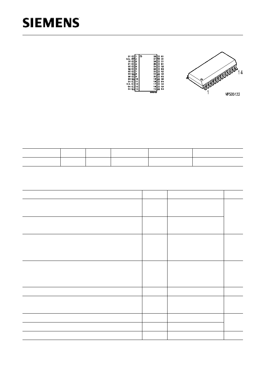
Type
V
DS
I
D
R
DS(on)
Package
Ordering Code
BUZ 100S-4
55 V
8 A
0.02
P-DSO-28
C67078-S. . . . -A..
Maximum Ratings
Parameter
Symbol
Values
Unit
Continuous drain current
one channel active
T
A
= 25 ∞C
I
D
8
A
Pulsed drain current
one channel active
T
A
= 25 ∞C
I
Dpuls
32
Avalanche energy, single pulse
I
D
= 8 A,
V
DD
= 25 V,
R
GS
= 25
L
= 11.8 mH,
T
j
= 25 ∞C
E
AS
380
mJ
Reverse diode d
v
/d
t
I
S
= 8 A,
V
DS
= 40 V, d
i
F
/d
t
= 200 A/µs
T
jmax
= 175 ∞C
d
v
/d
t
6
kV/µs
Gate source voltage
V
GS
±
20
V
Power dissipation
,one channel active
T
A
= 25 ∞C
P
tot
2.4
W
Operating temperature
T
j
-55 ... + 175
∞C
Storage temperature
T
stg
-55 ... + 175
IEC climatic category, DIN IEC 68-1
55 / 175 / 56

Semiconductor Group
2
01/Oct/1997
BUZ 100S-4
Preliminary data
Thermal Characteristics
Parameter
Symbol
Values
Unit
min.
typ.
max.
Thermal resistance, junction - soldering point
1)
R
thJS
-
-
tbd
K/W
Thermal resistance, junction - ambient
2)
R
thJA
-
-
62.5
1) Device on 50mm*50mm*1.5mm epoxy PCB FR4 with 6 cm
2
(one layer,70µm thick) copper area for
Drain connection. PCB is vertical without blown air.
2) one channel active
Electrical Characteristics, at
T
j
= 25∞C, unless otherwise specified
Parameter
Symbol
Values
Unit
min.
typ.
max.
Static Characteristics
Drain- source breakdown voltage
V
GS
= 0 V,
I
D
= 0.25 mA,
T
j
= 25 ∞C
V
(BR)DSS
55
-
-
V
Gate threshold voltage
V
GS=
V
DS,
I
D
= 130 µA
V
GS(th)
2.1
3
4
Zero gate voltage drain current
V
DS
= 55 V,
V
GS
= 0 V,
T
j
= -40 ∞C
V
DS
= 55 V,
V
GS
= 0 V,
T
j
= 25 ∞C
V
DS
= 55 V,
V
GS
= 0 V,
T
j
= 150 ∞C
I
DSS
-
-
-
-
0.1
-
100
1
0.1
µA
Gate-source leakage current
V
GS
= 20 V,
V
DS
= 0 V
I
GSS
-
10
100
nA
Drain-Source on-resistance
V
GS
= 10 V,
I
D
= 8 A
R
DS(on)
-
0.016
0.02

Semiconductor Group
3
01/Oct/1997
BUZ 100S-4
Preliminary data
Electrical Characteristics, at
T
j
= 25∞C, unless otherwise specified
Parameter
Symbol
Values
Unit
min.
typ.
max.
Dynamic Characteristics
Transconductance
V
DS
2
*
I
D *
R
DS(on)max,
I
D
= 8 A
g
fs
15
-
-
S
Input capacitance
V
GS
= 0 V,
V
DS
= 25 V,
f
= 1 MHz
C
iss
-
1900
2375
pF
Output capacitance
V
GS
= 0 V,
V
DS
= 25 V,
f
= 1 MHz
C
oss
-
615
770
Reverse transfer capacitance
V
GS
= 0 V,
V
DS
= 25 V,
f
= 1 MHz
C
rss
-
310
390
Turn-on delay time
V
DD
= 30 V,
V
GS
= 10 V,
I
D
= 8 A
R
G
= 4.6
t
d(on)
-
25
40
ns
Rise time
V
DD
= 30 V,
V
GS
= 10 V,
I
D
= 8 A
R
G
= 4.6
t
r
-
25
40
Turn-off delay time
V
DD
= 30 V,
V
GS
= 10 V,
I
D
= 8 A
R
G
= 4.6
t
d(off)
-
75
115
Fall time
V
DD
= 30 V,
V
GS
= 10 V,
I
D
= 8 A
R
G
= 4.6
t
f
-
35
55
Gate charge at threshold
V
DD
= 40 V,
I
D
0.1 A,
V
GS
=0 to 1 V
Q
g(th)
-
3.8
5.7
nC
Gate charge at 7.0 V
V
DD
= 40 V,
I
D
= 8 A,
V
GS
=0 to 7 V
Q
g(7)
-
50
75
Gate charge total
V
DD
= 40 V,
I
D
= 8 A,
V
GS
=0 to 10 V
Q
g(total)
-
63
95
Gate plateau voltage
V
DD
= 40 V,
I
D
= 8 A
V
(plateau)
-
4.43
-
V

Semiconductor Group
4
01/Oct/1997
BUZ 100S-4
Preliminary data
Electrical Characteristics, at
T
j
= 25∞C, unless otherwise specified
Parameter
Symbol
Values
Unit
min.
typ.
max.
Reverse Diode
Inverse diode continuous forward current
T
A
= 25 ∞C
I
S
-
-
8
A
Inverse diode direct current, pulsed
T
A
= 25 ∞C
I
SM
-
-
32
Inverse diode forward voltage
V
GS
= 0 V,
I
F
= 16 A
V
SD
-
0.95
1.6
V
Reverse recovery time
V
R
= 30 V,
I
F=
l
S,
d
i
F
/d
t
= 100 A/µs
t
rr
-
70
105
ns
Reverse recovery charge
V
R
= 30 V,
I
F=
l
S,
d
i
F
/d
t
= 100 A/µs
Q
rr
-
0.2
0.3
µC
Semiconductor Group
5
01/Oct/1997
BUZ 100S-4
Preliminary data
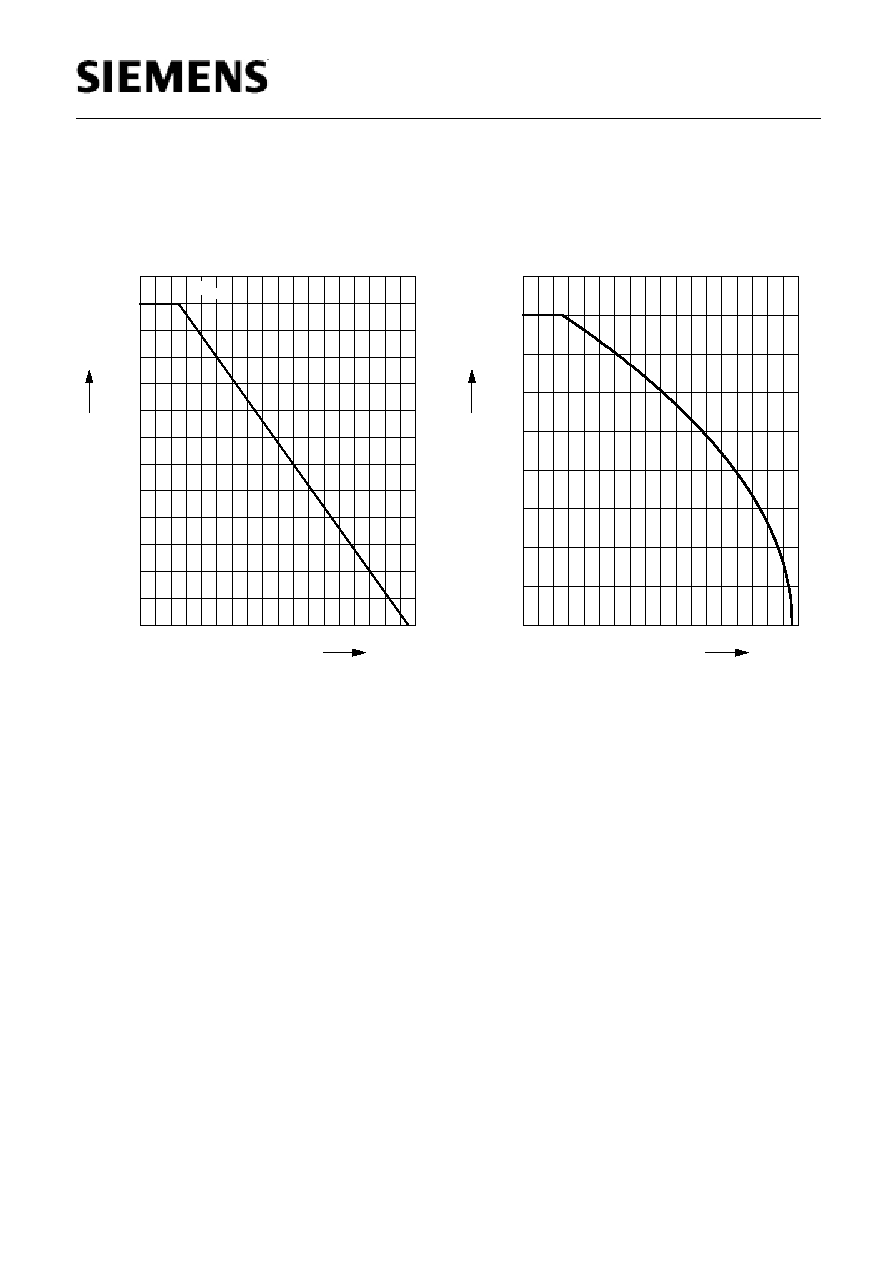
Power dissipation
P
tot
=
(T)
0
20
40
60
80
100 120 140
∞C
180
T
0.0
0.2
0.4
0.6
0.8
1.0
1.2
1.4
1.6
1.8
2.0
2.2
W
2.6
P
tot
R
thJC
R
thJA
Drain current
I
D
=
(T
C
)
parameter: V
GS
10 V
0
20
40
60
80
100 120 140
∞C
180
T
C
0
1
2
3
4
5
6
7
A
9
I
D
Semiconductor Group
6
01/Oct/1997
Preliminary data
BUZ 100S-4
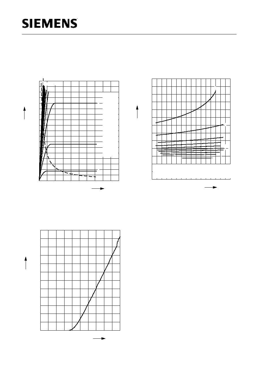
Typ. drain-source on-resistance
R
DS (on)
=
(
I
D
)
parameter: t
p
= 80 µs, T
j
= 25 ∞C
0
2
4
6
8
10
12
A
16
I
D
0.000
0.005
0.010
0.015
0.020
0.025
0.030
0.035
0.040
0.045
0.050
0.055
0.065
R
DS (on)
V
GS
[V] =
a
4.0
V
GS
[V] =
a
4.5
V
GS
[V] =
a
a
5.0
b
b
5.5
c
c
6.0
d
d
6.5
e
e
7.0
f
f
7.5
g
g
8.0
h
h
9.0
i
i
10.0
j
j
20.0
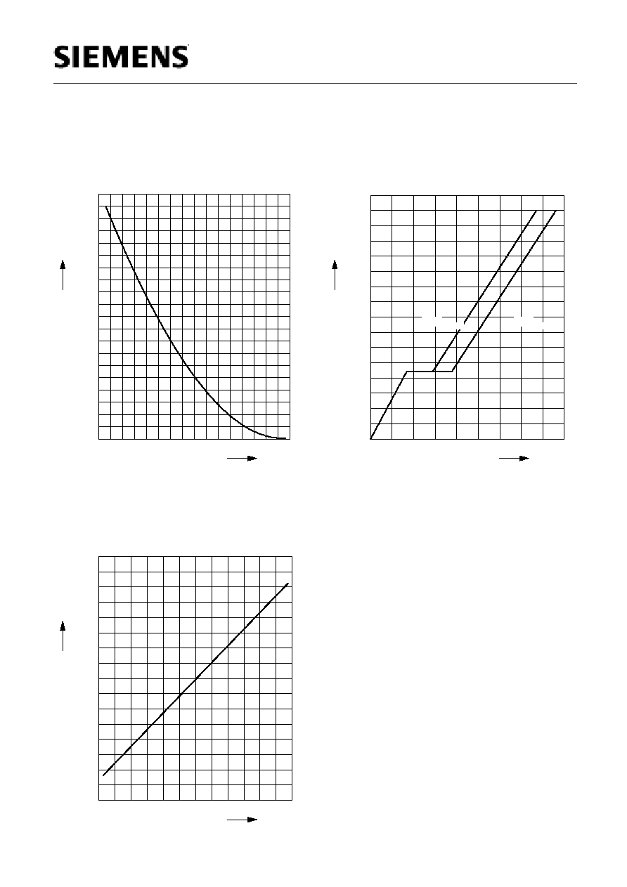
Typ. output characteristics
I
D
=
(
V
DS
)
parameter: t
p
= 80 µs
0.0
0.5
1.0
1.5
2.0
2.5
3.0
3.5
4.0
V
5.0
V
DS
0
2
4
6
8
10
12
14
A
18
I
D
V
GS
[V]
a
a
4.0
b
b
4.5
c
c
5.0
d
d
5.5
e
e
6.0
f
f
6.5
g
g
7.0
h
h
7.5
i
i
8.0
j
j
9.0
k
k
10.0
l
P
tot
= 2W
l
20.0
Typ. transfer characteristics I
D
= f (V
GS
)
parameter:
t
p
= 80 µs
V
DS
2 x
I
D
x
R
DS(on)max
0
1
2
3
4
5
6
7
8
V
10
V
GS
0
10
20
30
40
50
60
70
80
90
100
A
120
I
D
Semiconductor Group
7
01/Oct/1997
Preliminary data
BUZ 100S-4
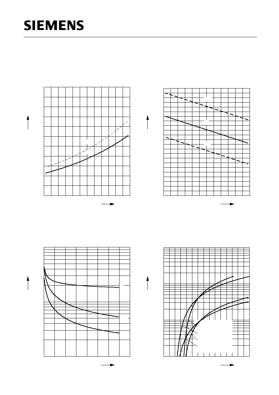
Drain-source on-resistance
R
DS (on)
=
(T
j
)
parameter: I
D
= 8 A, V
GS
= 10 V
-60
-20
20
60
100
∞C
180
T
j
0.000
0.005
0.010
0.015
0.020
0.025
0.030
0.035
0.040
0.045
0.055
R
DS (on)
typ
98%
Gate threshold voltage
V
GS (th)
=
(T
j
)
parameter: V
GS
= V
DS
, I
D
= 130 µA
0.0
0.4
0.8
1.2
1.6
2.0
2.4
2.8
3.2
3.6
4.0
V
4.6
V
GS(th)
-60
-20
20
60
100
∞C
180
T
j
2%
typ
98%
Typ. capacitances
C
=
f
(
V
DS
)
parameter:
V
GS
= 0V,
f
= 1MHz
0
5
10
15
20
25
30
V
40
V
DS
2
10
3
10
4
10
pF
C
C
iss
C
oss
C
rss
Forward characteristics of reverse diode
I
F
=
(V
SD
)
parameter: T
j
, t
p
= 80 µs
0
10
1
10
2
10
3
10
A
I
F
0.0
0.4
0.8
1.2
1.6
2.0
2.4
V
3.0
V
SD
T
j
= 25 ∞C typ
T
j
= 25 ∞C (98%)
T
j
= 175 ∞C typ
T
j
= 175 ∞C (98%)
Semiconductor Group
8
01/Oct/1997
Preliminary data
BUZ 100S-4
Avalanche energy E
AS
=
(T
j
)
parameter: I
D
= 8 A, V
DD
= 25 V
R
GS
= 25
, L = 11.8 mH
20
40
60
80
100
120
140
∞C
180
T
j
0
40
80
120
160
200
240
280
320
mJ
400
E
AS
Typ. gate charge
V
GS
=
(Q
Gate
)
parameter: I
D puls
= 8 A
0
10
20
30
40
50
60
70
nC
90
Q
Gate
0
2
4
6
8
10
12
V
16
V
GS
DS max
V
0,8
DS max
V
0,2
Drain-source breakdown voltage
V
(BR)DSS
=
(T
j
)
-60
-20
20
60
100
∞C
180
T
j
49
51
53
55
57
59
61
V
65
V
(BR)DSS