
N e v e r s t o p t h i n k i n g .
M i c r o c o n t r o l l e r s
D a t a S h e e t , V 3 . 0 , J a n . 2 0 0 1
C 1 6 1 C S - 3 2 R / - L
C 1 6 1 J C - 3 2 R / - L
C 1 6 1 J I - 3 2 R / - L
1 6 - B i t S i n g l e - C h i p M i c r o c o n t r o l l e r

Edition 2001-01
Published by Infineon Technologies AG,
St.-Martin-Strasse 53,
D-81541 M�nchen, Germany
�
Infineon Technologies AG 2001.
All Rights Reserved.
Attention please!
The information herein is given to describe certain components and shall not be considered as warranted
characteristics.
Terms of delivery and rights to technical change reserved.
We hereby disclaim any and all warranties, including but not limited to warranties of non-infringement, regarding
circuits, descriptions and charts stated herein.
Infineon Technologies is an approved CECC manufacturer.
Information
For further information on technology, delivery terms and conditions and prices please contact your nearest
Infineon Technologies Office in Germany or our Infineon Technologies Representatives worldwide.
Warnings
Due to technical requirements components may contain dangerous substances. For information on the types in
question please contact your nearest Infineon Technologies Office.
Infineon Technologies Components may only be used in life-support devices or systems with the express written
approval of Infineon Technologies, if a failure of such components can reasonably be expected to cause the failure
of that life-support device or system, or to affect the safety or effectiveness of that device or system. Life support
devices or systems are intended to be implanted in the human body, or to support and/or maintain and sustain
and/or protect human life. If they fail, it is reasonable to assume that the health of the user or other persons may
be endangered.

M i c r o c o n t r o l l e r s
D a t a S h e e t , V 3 . 0 , J a n . 2 0 0 1
N e v e r s t o p t h i n k i n g .
C 1 6 1 C S - 3 2 R / - L
C 1 6 1 J C - 3 2 R / - L
C 1 6 1 J I - 3 2 R / - L
1 6 - B i t S i n g l e - C h i p M i c r o c o n t r o l l e r
Controller Area Network (CAN): License of Robert Bosch GmbH
C161CS/JC/JI
Revision History:
2001-01
V3.0
Previous Version:
2000-08 V2.0 (intermediate version)
1999-03
(Advance Information)
Page
Subjects (major changes since last revision)
1)
1)
Changes refer to version 1999-03.
All
Converted to Infineon layout
2
Derivative Synopsis Table updated
4
,
6
,
10
,
18
Programmable Interface Routing introduced
27
,
28
GPT block diagrams updated
29
RTC description improved
35
OWD description improved
39
ff
RSTCON and SDLM registers added
51
Description of input/output voltage and hysteresis improved
53
Separate table for power consumption
57
Clock generation mode table updated
60
External clock drive specification improved
62
Reset calibration time specified, definition of
V
AREF
improved
63
Programmable sample time introduced
65
ff
Timing tables updated to 25 MHz
We Listen to Your Comments
Any information within this document that you feel is wrong, unclear or missing at all?
Your feedback will help us to continuously improve the quality of this document.
Please send your proposal (including a reference to this document) to:
mcdocu.comments@infineon.com

Data Sheet
1
V3.0, 2001-01
C161CS/JC/JI
16-Bit Single-Chip Microcontroller
C166 Family
C161CS/JC/JI
� High Performance 16-bit CPU with 4-Stage Pipeline
� 80 ns Instruction Cycle Time at 25 MHz CPU Clock
� 400 ns Multiplication (16
�
16 bit), 800 ns Division (32 / 16 bit)
� Enhanced Boolean Bit Manipulation Facilities
� Additional Instructions to Support HLL and Operating Systems
� Register-Based Design with Multiple Variable Register Banks
� Single-Cycle Context Switching Support
� 16 MBytes Total Linear Address Space for Code and Data
� 1024 Bytes On-Chip Special Function Register Area
� 16-Priority-Level Interrupt System with 59 Sources, Sample-Rate down to 40 ns
� 8-Channel Interrupt-Driven Single-Cycle Data Transfer Facilities via
Peripheral Event Controller (PEC)
� Clock Generation via on-chip PLL (factors 1:1.5/2/2.5/3/4/5),
via prescaler or via direct clock input
� Additional 32 kHz Oscillator
� On-Chip Memory Modules
� 2 KBytes On-Chip Internal RAM (IRAM)
� 8 KBytes On-Chip Extension RAM (XRAM)
� 256 KBytes On-Chip Mask ROM
� On-Chip Peripheral Modules
� 12-Channel 10-bit A/D Converter with Programmable Conversion Time
down to 7.8
�
s
� Two 16-Channel Capture/Compare Units (eight IO lines each)
� Two Multi-Functional General Purpose Timer Units with 5 Timers
� Two Asynchronous/Synchronous Serial Channels
� High-Speed Synchronous Serial Channel (SPI)
� On-Chip CAN Interface (Rev. 2.0B active, Full CAN / Basic CAN)
with 15 Message Objects (C161CS 2x, C161JC 1x)
� Serial Data Link Module (SDLM), compliant with J1850,
supporting Class 2 (C161JC/JI)
� IIC Bus Interface (10-bit Addressing, 400 kHz) with 2 Channels (multiplexed)
� On-Chip Real Time Clock
� Up to 16 MBytes External Address Space for Code and Data
� Programmable External Bus Characteristics for Different Address Ranges
� Multiplexed or Demultiplexed External Address/Data Buses with 8-Bit or 16-Bit
Data Bus Width
� Five Programmable Chip-Select Signals
� Hold- and Hold-Acknowledge Bus Arbitration Support

C161CS/JC/JI-32R
C161CS/JC/JI-L
Data Sheet
2
V3.0, 2001-01
� Idle, Sleep, and Power Down Modes with Flexible Power Management
� Programmable Watchdog Timer and Oscillator Watchdog
� Up to 93 General Purpose I/O Lines,
partly with Selectable Input Thresholds and Hysteresis
� Supported by a Large Range of Development Tools like C-Compilers,
Macro-Assembler Packages, Emulators, Evaluation Boards, HLL-Debuggers,
Simulators, Logic Analyzer Disassemblers, Programming Boards
� On-Chip Bootstrap Loader
� 128-Pin TQFP Package
This document describes several derivatives of the C161 group.
Table 1
enumerates
these derivatives and summarizes the differences. As this document refers to all of these
derivatives, some descriptions may not apply to a specific product.
For simplicity all versions are referred to by the term C161CS/JC/JI throughout this
document.
Table 1
C161CS/JC/JI Derivative Synopsis
Derivative
On-Chip
Program Memory
Serial Bus
Interface(s)
Maximum CPU
Frequency
SAK-C161CS-32RF
SAB-C161CS-32RF
256 KByte ROM
CAN1, CAN2
25 MHz
SAK-C161CS-LF
SAB-C161CS-LF
---
CAN1, CAN2
25 MHz
SAK-C161JC-32RF
SAB-C161JC-32RF
256 KByte ROM
CAN1, SDLM
25 MHz
SAK-C161JC-LF
SAB-C161JC-LF
---
CAN1, SDLM
25 MHz
SAK-C161JI-32RF
SAB-C161JI-32RF
256 KByte ROM
SDLM
25 MHz
SAK-C161JI-LF
SAB-C161JI-LF
---
SDLM
25 MHz
C161CS/JC/JI-32R
C161CS/JC/JI-L
Data Sheet
3
V3.0, 2001-01
Ordering Information
The ordering code for Infineon microcontrollers provides an exact reference to the
required product. This ordering code identifies:
� the derivative itself, i.e. its function set, the temperature range, and the supply voltage
� the package and the type of delivery.
For the available ordering codes for the C161CS/JC/JI please refer to the "Product
Catalog Microcontrollers", which summarizes all available microcontroller variants.
Note: The ordering codes for Mask-ROM versions are defined for each product after
verification of the respective ROM code.
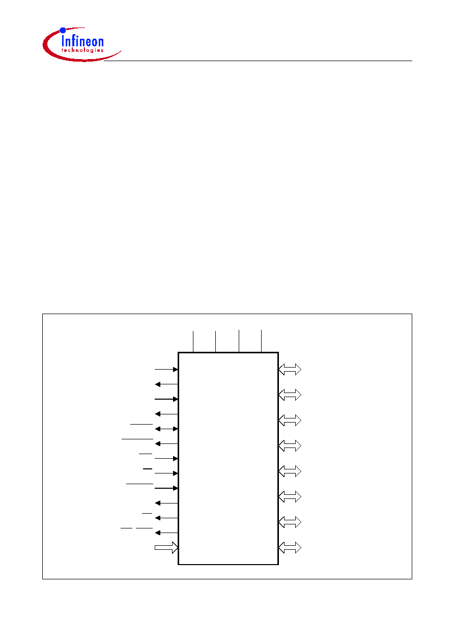
Introduction
The C161CS/JC/JI derivatives are high performance derivatives of the Infineon
C166 Family of full featured single-chip CMOS microcontrollers. They combine high
CPU performance (up to 12.5 million instructions per second) with high peripheral
functionality and enhanced IO-capabilities. They also provide clock generation via PLL
and various on-chip memory modules such as program ROM, internal RAM, and
extension RAM.
Figure 1
Logic Symbol
MCL04450
C161CS/JC/JI
V
AGND
V
DD
V
SS
V
AREF
XTAL1
XTAL2
Port 0
16 Bit
XTAL4
XTAL3
Port 1
16 Bit
Port 2
8 Bit
Port 3
15 Bit
Port 4
8 Bit
Port 6
8 Bit
Port 7
4 Bit
Port 9
6 Bit
RSTIN
RSTOUT
NMI
EA
READY
ALE
RD
WR/WRL
Port 5
12 Bit
C161CS/JC/JI-32R
C161CS/JC/JI-L
Data Sheet
4
V3.0, 2001-01
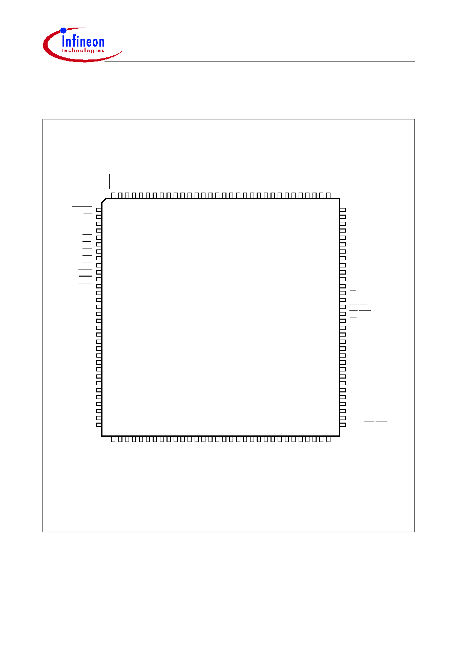
Pin Configuration
(top view)
Figure 2
*) The marked pins of Port 4 and Port 7 can have interface lines assigned to them (CAN
interface in the C161CS and C161JC, SDLM interface in the C161JC and C161JI).
Table 2
on the pages below lists the possible assignments.
MCP04451
RSTOUT
1
NMI
2
V
SS
3
4
5
P6.0/CS0
6
7
8
9
10
11
12
13
14
15
16
17
V
SS
18
19
P9.0/SDA0
20
21
22
23
P9.5
24
25
26
P5.0/AN0
27
28
29
P5.2/AN2
30
31
32
P5.6/AN6
33
34
V
AREF
35
36
37
P5.12/AN12/T6IN
38
39
40
V
SS
41
42
43
P2.8/CC8IO/EX0IN
44
45
46
47
48
49
50
V
SS
51
52
P3.0/T0IN/TxD1
53
54
55
P3.2/CAPIN
P3.3/T3OUT
56
P3.4/T3EUD
57
58
P3.5/T4IN
P3.6/T3IN
59
P3.7/T2IN
60
61
P3.8/MRST
P3.9/MTSR
62
P3.10/TxD0
63
64
P3.11/RxD0
RSTIN
128
XT
AL4
127
65
P3.12/BHE/WRH
P3.13/SCLK
66
67
P3.15/CLKOUT/FOUT
V
DD
68
69
70
P4.0/A16
P4.1/A17
71
72
73
74
75
76
77
V
DD
78
79
RD
80
WR/WRL
81
82
READY
ALE
83
EA
84
85
P0L.0/AD0
86
87
88
89
90
91
92
V
DD
93
94
P0H.0/AD8
95
P0H.1/AD9
96
126
XT
AL3
125
XT
AL1
124
123
XT
AL2
122
V
DD
121
120
119
118
117
P1H.4/A12/CC24IO
116
115
114
P1H.0/A8
113
112
111
V
DD
110
109
108
107
106
105
104
P1L.0/A0
103
102
101
100
99
P0H.4/AD12
98
P0H.2/AD10
97
C161CS/JC/JI
V
DD
P6.1/CS1
P6.2/CS2
P6.3/CS3
P6.4/CS4
P6.5/HOLD
P6.6/HLDA
P6.7/BREQ
P7.4/CC28IO/*
P7.5/CC29IO/*
P7.6/CC30IO/*
P7.7/CC31IO/*
V
DD
P9.1/SCL0
P9.2/SDA1
P9.3/SCL1
P9.4/SDA2
V
SS
V
DD
P5.1/AN1
P5.3/AN3
P5.4/AN4
P5.5/AN5
P5.7/AN7
V
A
GND
P5.13/AN13/T5IN
P5.14/AN14/T4EUD
P5.15/AN15/T2EUD
V
DD
P2.9/CC9IO/EX1IN
P2.10/CC10IO/EX2IN
P2.11/CC11IO/EX3IN
P2.12/CC12IO/EX4IN
P2.13/CC13IO/EX5IN
P2.14/CC14IO/EX6IN
P2.15/CC15IO/EX7INT7IN
V
DD
P3.1/T6OUT/RxD1
V
SS
P4.2/A18
P4.3/A19
P4.4/A20/*
P4.5/A21/*
P4.6/A22/*
P4.7/A23/*
V
SS
P0L.1/AD1
P0L.2/AD2
P0L.3/AD3
P0L.4/AD4
P0L.5/AD5
P0L.6/AD6
P0L.7/AD7
V
SS
P0H.3/AD11
P0H.5/AD13
P0H.6/AD14
P0H.7/AD15
P1L.1/A1
P1L.2/A2
P1L.3/A3
P1L.4/A4
P1L.5/A5
P1L.6/A6
P1L.7/A7
V
SS
P1H.1/A9
P1H.2/A10
P1H.3/A11
P1H.5/A13/CC25IO
P1H.6/A14/CC26IO
P1H.7/A15/CC27IO
V
SS
V
SS
C161CS/JC/JI-32R
C161CS/JC/JI-L
Data Sheet
5
V3.0, 2001-01
Table 2
Pin Definitions and Functions
Symbol Pin
No.
Input
Outp.
Function
RST
OUT
1
O
Internal Reset Indication Output. This pin is set to a low level
when the part is executing either a hardware-, a software- or
a watchdog timer reset. RSTOUT remains low until the EINIT
(end of initialization) instruction is executed.
NMI
2
I
Non-Maskable Interrupt Input. A high to low transition at this
pin causes the CPU to vector to the NMI trap routine. When
the PWRDN (power down) instruction is executed, the NMI
pin must be low in order to force the C161CS/JC/JI to go into
power down mode. If NMI is high, when PWRDN is
executed, the part will continue to run in normal mode.
If not used, pin NMI should be pulled high externally.
P6
P6.0
P6.1
P6.2
P6.3
P6.4
P6.5
P6.6
P6.7
5
6
7
8
9
10
11
12
IO
O
O
O
O
O
I
I/O
O
Port 6 is an 8-bit bidirectional I/O port. It is bit-wise
programmable for input or output via direction bits. For a pin
configured as input, the output driver is put into high-
impedance state. Port 6 outputs can be configured as push/
pull or open drain drivers.
The Port 6 pins also serve for alternate functions:
CS0
Chip Select 0 Output
CS1
Chip Select 1 Output
CS2
Chip Select 2 Output
CS3
Chip Select 3 Output
CS4
Chip Select 4 Output
HOLD
External Master Hold Request Input
HLDA
Hold Acknowledge Output (master mode)
or Input (slave mode)
BREQ
Bus Request Output

C161CS/JC/JI-32R
C161CS/JC/JI-L
Data Sheet
6
V3.0, 2001-01
P7
P7.4
P7.5
P7.6
P7.7
13
14
15
16
IO
I/O
I
I
O
I/O
O
O
I
I/O
I
I
O
I/O
O
O
I
Port 7 is a 4-bit bidirectional I/O port. It is bit-wise
programmable for input or output via direction bits. For a pin
configured as input, the output driver is put into high-
impedance state. Port 7 outputs can be configured as push/
pull or open drain drivers. The input threshold of Port 7 is
selectable (TTL or special). Port 7 pins provide inputs/
outputs for CAPCOM2 and serial interface lines.
1)
CC28IO
CAPCOM2: CC28 Capture Inp./Compare Outp.,
CAN1_RxD CAN 1 Receive Data Input,
(C161CS/JC)
CAN2_RxD CAN 2 Receive Data Input,
(C161CS)
SDL_TxD
SDLM Transmit Data Output
(C161JC/JI)
CC29IO
CAPCOM2: CC29 Capture Inp./Compare Outp.,
CAN1_TxD CAN 1 Transmit Data Output,
(C161CS/JC)
CAN2_TxD CAN 2 Transmit Data Output,
(C161CS)
SDL_RxD SDLM Receive Data Input
(C161JC/JI)
CC30IO
CAPCOM2: CC30 Capture Inp./Compare Outp.,
CAN1_RxD CAN 1 Receive Data Input,
(C161CS/JC)
CAN2_RxD CAN 2 Receive Data Input,
(C161CS)
SDL_TxD
SDLM Transmit Data Output
(C161JC/JI)
CC31IO
CAPCOM2: CC31 Capture Inp./Compare Outp.,
CAN1_TxD CAN 1 Transmit Data Output,
(C161CS/JC)
CAN2_TxD CAN 2 Transmit Data Output,
(C161CS)
SDL_RxD SDLM Receive Data Input
(C161JC/JI)
P9
P9.0
P9.1
P9.2
P9.3
P9.4
P9.5
19
20
21
22
23
24
IO
I/O
I/O
I/O
I/O
I/O
�
Port 9 is a 6-bit bidirectional open drain I/O port (provide
external pullup resistors if required). It is bit-wise
programmable for input or output via direction bits. For a pin
configured as input, the output driver is put into high-
impedance state.
The following Port 9 pins also serve for alternate functions:
SDA0
IIC Bus Data Line 0
SCL0
IIC Bus Clock Line 0
SDA1
IIC Bus Data Line 1
SCL1
IIC Bus Clock Line 1
SDA2
IIC Bus Data Line 2
�
Note: Port 9 pins can only tolerate positive overload currents
(see
Table 9
).
Table 2
Pin Definitions and Functions (cont'd)
Symbol Pin
No.
Input
Outp.
Function
C161CS/JC/JI-32R
C161CS/JC/JI-L
Data Sheet
7
V3.0, 2001-01
P5
P5.0
P5.1
P5.2
P5.3
P5.4
P5.5
P5.6
P5.7
P5.12
P5.13
P5.14
P5.15
27
28
29
30
31
32
33
34
37
38
39
40
I
I
I
I
I
I
I
I
I
I
I
I
I
Port 5 is a 12-bit input-only port with Schmitt-Trigger char.
The pins of Port 5 also serve as analog input channels for the
A/D converter, or they serve as timer inputs:
AN0
AN1
AN2
AN3
AN4
AN5
AN6
AN7
AN12,
T6IN
GPT2 Timer T6 Count Inp.
AN13,
T5IN
GPT2 Timer T5 Count Inp.
AN14,
T4EUD GPT1 Timer T4 Ext. Up/Down Ctrl. Inp.
AN15,
T2EUD GPT1 Timer T5 Ext. Up/Down Ctrl. Inp.
Table 2
Pin Definitions and Functions (cont'd)
Symbol Pin
No.
Input
Outp.
Function

C161CS/JC/JI-32R
C161CS/JC/JI-L
Data Sheet
8
V3.0, 2001-01
P2
P2.8
P2.9
P2.10
P2.11
P2.12
P2.13
P2.14
P2.15
43
44
45
46
47
48
49
50
IO
I/O
I
I/O
I
I/O
I
I/O
I
I/O
I
I/O
I
I/O
I
I/O
I
I
Port 2 is an 8-bit bidirectional I/O port. It is bit-wise
programmable for input or output via direction bits. For a pin
configured as input, the output driver is put into high-
impedance state. Port 2 outputs can be configured as push/
pull or open drain drivers. The input threshold of Port 2 is
selectable (TTL or special).
The following Port 2 pins also serve for alternate functions:
CC8IO
CAPCOM1: CC8 Capture Inp./Compare Output,
EX0IN
Fast External Interrupt 0 Input
CC9IO
CAPCOM1: CC9 Capture Inp./Compare Output,
EX1IN
Fast External Interrupt 1 Input
CC10IO
CAPCOM1: CC10 Capture Inp./Compare Outp.,
EX2IN
Fast External Interrupt 2 Input
CC11IO
CAPCOM1: CC11 Capture Inp./Compare Outp.,
EX3IN
Fast External Interrupt 3 Input
CC12IO
CAPCOM1: CC12 Capture Inp./Compare Outp.,
EX4IN
Fast External Interrupt 4 Input
CC13IO
CAPCOM1: CC13 Capture Inp./Compare Outp.,
EX5IN
Fast External Interrupt 5 Input
CC14IO
CAPCOM1: CC14 Capture Inp./Compare Outp.,
EX6IN
Fast External Interrupt 6 Input
CC15IO
CAPCOM1: CC15 Capture Inp./Compare Outp.,
EX7IN
Fast External Interrupt 7 Input,
T7IN
CAPCOM2: Timer T7 Count Input
Note: During Sleep Mode a spike filter on the EXnIN
interrupt inputs suppresses input pulses < 10 ns.
Input pulses > 100 ns safely pass the filter.
Table 2
Pin Definitions and Functions (cont'd)
Symbol Pin
No.
Input
Outp.
Function
C161CS/JC/JI-32R
C161CS/JC/JI-L
Data Sheet
9
V3.0, 2001-01
P3
P3.0
P3.1
P3.2
P3.3
P3.4
P3.5
P3.6
P3.7
P3.8
P3.9
P3.10
P3.11
P3.12
P3.13
P3.15
53
54
55
56
57
58
59
60
61
62
63
64
65
66
67
IO
I
O
O
I/O
I
O
I
I
I
I
I/O
I/O
O
I/O
O
O
I/O
O
O
Port 3 is a 15-bit bidirectional I/O port. It is bit-wise
programmable for input or output via direction bits. For a pin
configured as input, the output driver is put into high-
impedance state. Port 3 outputs can be configured as push/
pull or open drain drivers. The input threshold of Port 3 is
selectable (TTL or special).
The following Port 3 pins also serve for alternate functions:
T0IN
CAPCOM1 Timer T0 Count Input,
TxD1
ASC1 Clock/Data Output (Async./Sync)
T6OUT
GPT2 Timer T6 Toggle Latch Output,
RxD1
ASC1 Data Input (Async.) or Inp./Output (Sync.)
CAPIN
GPT2 Register CAPREL Capture Input
T3OUT
GPT1 Timer T3 Toggle Latch Output
T3EUD
GPT1 Timer T3 External Up/Down Control Input
T4IN
GPT1 Timer T4 Count/Gate/Reload/Capture Inp
T3IN
GPT1 Timer T3 Count/Gate Input
T2IN
GPT1 Timer T2 Count/Gate/Reload/Capture Inp
MRST
SSC Master-Receive/Slave-Transmit Inp./Outp.
MTSR
SSC Master-Transmit/Slave-Receive Outp./Inp.
TxD0
ASC0 Clock/Data Output (Async./Sync.)
RxD0
ASC0 Data Input (Async.) or Inp./Outp. (Sync.)
BHE
External Memory High Byte Enable Signal,
WRH
External Memory High Byte Write Strobe
SCLK
SSC Master Clock Output / Slave Clock Input.
CLKOUT
System Clock Output (= CPU Clock)
FOUT
Programmable Frequency Output
Table 2
Pin Definitions and Functions (cont'd)
Symbol Pin
No.
Input
Outp.
Function

C161CS/JC/JI-32R
C161CS/JC/JI-L
Data Sheet
10
V3.0, 2001-01
P4
P4.0
P4.1
P4.2
P4.3
P4.4
P4.5
P4.6
P4.7
70
71
72
73
74
75
76
77
IO
O
O
O
O
O
I
I
O
I
O
O
O
I
O
I
O
I
O
Port 4 is an 8-bit bidirectional I/O port. It is bit-wise
programmable for input or output via direction bits. For a pin
configured as input, the output driver is put into high-
impedance state. The Port 4 outputs can be configured as
push/pull or open drain drivers. The input threshold of Port 4
is selectable (TTL or special).
Port 4 can be used to output the segment address lines and
for serial interface lines:
1)
A16
Least Significant Segment Address Line
A17
Segment Address Line
A18
Segment Address Line
A19
Segment Address Line
A20
Segment Address Line,
CAN2_RxD CAN 2 Receive Data Input,
(C161CS)
SDL_RxD SDLM Receive Data Input
(C161JC/JI)
A21
Segment Address Line,
CAN1_RxD CAN 1 Receive Data Input,
(C161CS/JC)
A22
Segment Address Line,
CAN1_TxD CAN 1 Transmit Data Output,
(C161CS/JC)
CAN2_TxD CAN 2 Transmit Data Output,
(C161CS)
SDL_RxD SDLM Receive Data Input
(C161JC/JI)
A23
Most Significant Segment Address Line,
CAN1_RxD CAN 1 Receive Data Input,
(C161CS/JC)
CAN2_TxD CAN 2 Transmit Data Output,
(C161CS)
CAN2_RxD CAN 2 Receive Data Input,
(C161CS)
SDL_TxD
SDLM Transmit Data Output
(C161JC/JI)
RD
80
O
External Memory Read Strobe. RD is activated for every
external instruction or data read access.
WR/
WRL
81
O
External Memory Write Strobe. In WR-mode this pin is
activated for every external data write access. In WRL-mode
this pin is activated for low byte data write accesses on a
16-bit bus, and for every data write access on an 8-bit bus.
See WRCFG in register SYSCON for mode selection.
Table 2
Pin Definitions and Functions (cont'd)
Symbol Pin
No.
Input
Outp.
Function

C161CS/JC/JI-32R
C161CS/JC/JI-L
Data Sheet
11
V3.0, 2001-01
READY 82
I
Ready Input. When the Ready function is enabled, a high
level at this pin during an external memory access will force
the insertion of memory cycle time waitstates until the pin
returns to a low level.
An internal pullup device will hold this pin high when nothing
is driving it.
ALE
83
O
Address Latch Enable Output. Can be used for latching the
address into external memory or an address latch in the
multiplexed bus modes.
EA
84
I
External Access Enable pin. A low level at this pin during and
after Reset forces the C161CS/JC/JI to begin instruction
execution out of external memory. A high level forces
execution out of the internal program memory.
"ROMless" versions must have this pin tied to `0'.
PORT0
P0L.0-7
P0H.0-7
85-
92
95-
102
IO
PORT0 consists of the two 8-bit bidirectional I/O ports P0L
and P0H. It is bit-wise programmable for input or output via
direction bits. For a pin configured as input, the output driver
is put into high-impedance state.
In case of an external bus configuration, PORT0 serves as
the address (A) and address/data (AD) bus in multiplexed
bus modes and as the data (D) bus in demultiplexed bus
modes.
Demultiplexed bus modes:
Data Path Width:
8-bit
16-bit
P0L.0 � P0L.7:
D0 � D7
D0 - D7
P0H.0 � P0H.7:
I/O
D8 - D15
Multiplexed bus modes:
Data Path Width:
8-bit
16-bit
P0L.0 � P0L.7:
AD0 � AD7
AD0 - AD7
P0H.0 � P0H.7:
A8 - A15
AD8 - AD15
Note: At the end of an external reset (EA = `0') PORT0 also
inputs the configuration values.
Table 2
Pin Definitions and Functions (cont'd)
Symbol Pin
No.
Input
Outp.
Function

C161CS/JC/JI-32R
C161CS/JC/JI-L
Data Sheet
12
V3.0, 2001-01
PORT1
P1L.0-7
P1H.0-7
P1H.4
P1H.5
P1H.6
P1H.7
103-
110
113-
120
117
118
119
120
IO
I/O
I/O
I/O
I/O
PORT1 consists of the two 8-bit bidirectional I/O ports P1L
and P1H. It is bit-wise programmable for input or output via
direction bits. For a pin configured as input, the output driver
is put into high-impedance state. PORT1 is used as the
16-bit address bus (A) in demultiplexed bus modes and also
after switching from a demultiplexed bus mode to a
multiplexed bus mode.
The following PORT1 pins also serve for alternate functions:
CC24IO
CAPCOM2: CC24 Capture Inp./Compare Outp.
CC25IO
CAPCOM2: CC25 Capture Inp./Compare Outp.
CC26IO
CAPCOM2: CC26 Capture Inp./Compare Outp.
CC27IO
CAPCOM2: CC27 Capture Inp./Compare Outp.
XTAL2
XTAL1
123
124
O
I
XTAL2:
Output of the oscillator amplifier circuit.
XTAL1:
Input to the oscillator amplifier and input to
the internal clock generator
To clock the device from an external source, drive XTAL1,
while leaving XTAL2 unconnected. Minimum and maximum
high/low and rise/fall times specified in the AC
Characteristics must be observed.
XTAL3
XTAL4
126
127
I
O
XTAL3:
Input to the 32-kHz oscillator amplifier and
input to the internal clock generator
XTAL4:
Output of the oscillator amplifier circuit.
To clock the device from an external source, drive XTAL3,
while leaving XTAL4 unconnected. Minimum and maximum
high/low and rise/fall times specified in the AC
Characteristics must be observed.
Table 2
Pin Definitions and Functions (cont'd)
Symbol Pin
No.
Input
Outp.
Function
C161CS/JC/JI-32R
C161CS/JC/JI-L
Data Sheet
13
V3.0, 2001-01
RSTIN
128
I/O
Reset Input with Schmitt-Trigger characteristics. A low level
at this pin while the oscillator is running resets the C161CS/
JC/JI. An internal pullup resistor permits power-on reset
using only a capacitor connected to
V
SS
.
A spike filter suppresses input pulses < 10 ns. Input pulses
> 100 ns safely pass the filter. The minimum duration for a
safe recognition should be 100 ns + 2 CPU clock cycles.
In bidirectional reset mode (enabled by setting bit BDRSTEN
in register SYSCON) the RSTIN line is internally pulled low
for the duration of the internal reset sequence upon any reset
(HW, SW, WDT). See note below this table.
Note: To let the reset configuration of PORT0 settle and to
let the PLL lock a reset duration of ca. 1 ms is
recommended.
V
AREF
35
�
Reference voltage for the A/D converter.
V
AGND
36
�
Reference ground for the A/D converter.
V
DD
4, 18,
26
2)
,
42, 52,
68, 78,
93, 111,
121
�
Digital Supply Voltage:
+5 V during normal operation and idle mode.
2.5 V during power down mode if RTC is off
2.7 V during power down mode if RTC is running
V
SS
3, 17,
25
2)
,
41, 51,
69, 79,
94, 112,
122,
125
�
Digital Ground.
1)
The CAN and/or SDLM interface lines are assigned to ports P4 and P7 under software control. Within the CAN
module or SDLM several assignments can be selected.
2)
Supply pins 25 and 26 feed the Analog/Digital Converter and should be decoupled separately.
Table 2
Pin Definitions and Functions (cont'd)
Symbol Pin
No.
Input
Outp.
Function

C161CS/JC/JI-32R
C161CS/JC/JI-L
Data Sheet
14
V3.0, 2001-01
Note: The following behavioural differences must be observed when the bidirectional
reset is active:
� Bit BDRSTEN in register SYSCON cannot be changed after EINIT and is cleared
automatically after a reset.
� The reset indication flags always indicate a long hardware reset.
� The PORT0 configuration is treated as if it were a hardware reset. In particular, the
bootstrap loader may be activated when P0L.4 is low.
� Pin RSTIN may only be connected to external reset devices with an open drain output
driver.
� A short hardware reset is extended to the duration of the internal reset sequence.
C161CS/JC/JI-32R
C161CS/JC/JI-L
Data Sheet
15
V3.0, 2001-01
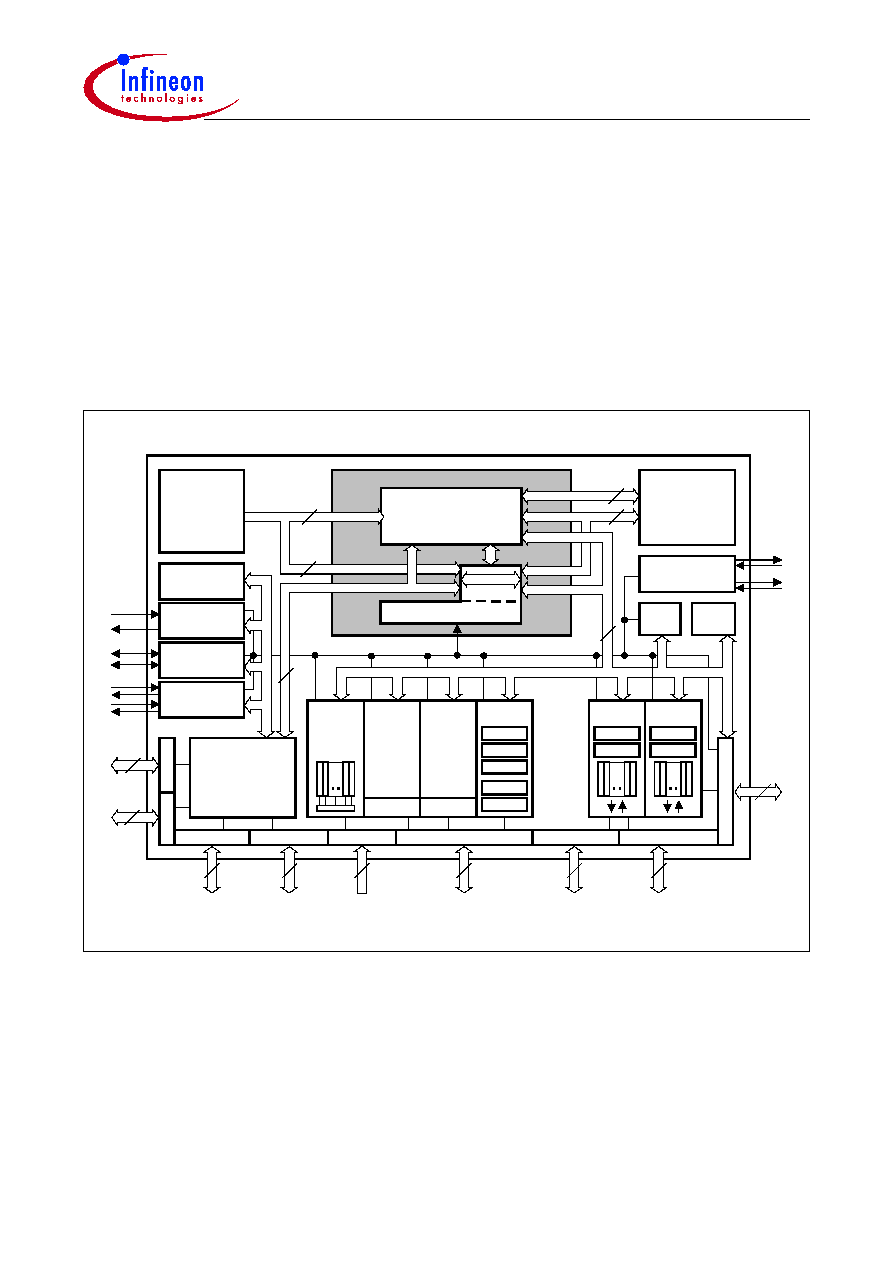
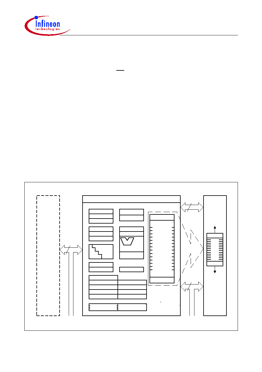
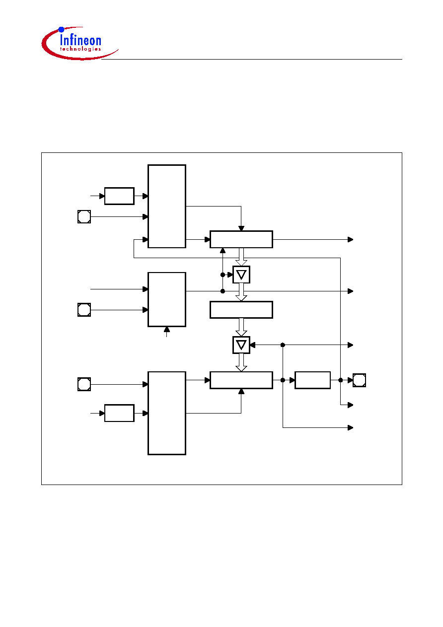
Functional Description
The architecture of the C161CS/JC/JI combines advantages of both RISC and CISC
processors and of advanced peripheral subsystems in a very well-balanced way. In
addition the on-chip memory blocks allow the design of compact systems with maximum
performance.
The following block diagram gives an overview of the different on-chip components and
of the advanced, high bandwidth internal bus structure of the C161CS/JC/JI.
Note: All time specifications refer to a CPU clock of 25 MHz
(see definition in the AC Characteristics section).
Figure 3
Block Diagram
The program memory, the internal RAM (IRAM) and the set of generic peripherals are
connected to the CPU via separate buses. A fourth bus, the XBUS, connects external
resources as well as additional on-chip resoures, the X-Peripherals (see
Figure 3
).
The XBUS resources (XRAM, CAN, SDLM, IIC, ASC1) of the C161CS/JC/JI can be
enabled during initialization by setting the general X-Peripheral enable bit XPEN
(SYSCON.2).
If the X-Peripherals remain disabled they consume neither address space nor port pins.
C166-Core
CPU
Port 2
Interrupt Bus
XTAL
Osc / PLL
RTC
WDT
32
16
Interrupt Controller 16-Level
Priority
PEC
External Instr. / Data
GPT
T2
T3
T4
T5
T6
SSC
BRGen
(SPI)
ASC0
BRGen
(USART)
ADC
10-Bit
12
Channels
CCOM1
T0
T1
CCOM2
T7
T8
EBC
XBUS Control
External Bus
Control
IRAM
Dual Port
Internal
RAM
2 KByte
ProgMem
ROM
256 KByte
Data
Data
16
16
16
CAN/SDLM
2.0B act. / Cl.B
Instr. / Data
Port 0
XRAM
8 KByte
Port 6
8
8
Port 1
16
12
16
Port 5
Port 3
15
Port 7
4
Port 9
6
Port 4
8
Peripheral Data Bus
ASC1
(USART)
IIC
400 KBd, 2 Ch.
16
On-Chip XBUS (16-Bit Demux)
MCB04323_1CSR

C161CS/JC/JI-32R
C161CS/JC/JI-L
Data Sheet
16
V3.0, 2001-01
Memory Organization
The memory space of the C161CS/JC/JI is configured in a Von Neumann architecture
which means that code memory, data memory, registers and I/O ports are organized
within the same linear address space which includes 16 MBytes. The entire memory
space can be accessed bytewise or wordwise. Particular portions of the on-chip memory
have additionally been made directly bitaddressable.
The C161CS/JC/JI incorporates 256 KBytes of on-chip mask-programmable ROM for
code or constant data. The lower 32 KBytes of the on-chip ROM can be mapped either
to segment 0 or segment 1.
2 KBytes of on-chip Internal RAM (IRAM) are provided as a storage for user defined
variables, for the system stack, general purpose register banks and even for code. A
register bank can consist of up to 16 wordwide (R0 to R15) and/or bytewide (RL0, RH0,
..., RL7, RH7) so-called General Purpose Registers (GPRs).
1024 bytes (2
�
512 bytes) of the address space are reserved for the Special Function
Register areas (SFR space and ESFR space). SFRs are wordwide registers which are
used for controlling and monitoring functions of the different on-chip units. Unused SFR
addresses are reserved for future members of the C166 Family.
8 KBytes of on-chip Extension RAM (XRAM) are provided to store user data, user
stacks, or code. The XRAM is accessed like external memory and therefore cannot be
used for the system stack or for register banks and is not bitaddressable. The XRAM
permits 16-bit accesses with maximum speed.
In order to meet the needs of designs where more memory is required than is provided
on chip, up to 16 MBytes of external RAM and/or ROM can be connected to the
microcontroller.

C161CS/JC/JI-32R
C161CS/JC/JI-L
Data Sheet
17
V3.0, 2001-01
External Bus Controller
All of the external memory accesses are performed by a particular on-chip External Bus
Controller (EBC). It can be programmed either to Single Chip Mode when no external
memory is required, or to one of four different external memory access modes, which
are as follows:
� 16-/18-/20-/24-bit Addresses, 16-bit Data, Demultiplexed
� 16-/18-/20-/24-bit Addresses, 16-bit Data, Multiplexed
� 16-/18-/20-/24-bit Addresses, 8-bit Data, Multiplexed
� 16-/18-/20-/24-bit Addresses, 8-bit Data, Demultiplexed
In the demultiplexed bus modes, addresses are output on PORT1 and data is input/
output on PORT0 or P0L, respectively. In the multiplexed bus modes both addresses
and data use PORT0 for input/output.
Important timing characteristics of the external bus interface (Memory Cycle Time,
Memory Tri-State Time, Length of ALE and Read Write Delay) have been made
programmable to allow the user the adaption of a wide range of different types of
memories and external peripherals.
In addition, up to 4 independent address windows may be defined (via register pairs
ADDRSELx / BUSCONx) which control the access to different resources with different
bus characteristics. These address windows are arranged hierarchically where
BUSCON4 overrides BUSCON3 and BUSCON2 overrides BUSCON1. All accesses to
locations not covered by these 4 address windows are controlled by BUSCON0.
Up to 5 external CS signals (4 windows plus default) can be generated in order to save
external glue logic. The C161CS/JC/JI offers the possibility to switch the CS outputs to
an unlatched mode. In this mode the internal filter logic is switched off and the CS signals
are directly generated from the address. The unlatched CS mode is enabled by setting
CSCFG (SYSCON.6).
Access to very slow memories or memories with varying access times is supported via
a particular `Ready' function.
A HOLD/HLDA protocol is available for bus arbitration and allows to share external
resources with other bus masters. The bus arbitration is enabled by setting bit HLDEN
in register PSW. After setting HLDEN once, pins P6.7 ... P6.5 (BREQ, HLDA, HOLD)
are automatically controlled by the EBC. In Master Mode (default after reset) the HLDA
pin is an output. By setting bit DP6.7 to `1' the Slave Mode is selected where pin HLDA
is switched to input. This allows to directly connect the slave controller to another master
controller without glue logic.
For applications which require less than 16 MBytes of external memory space, this
address space can be restricted to 1 MByte, 256 KByte, or to 64 KByte. In this case
Port 4 outputs four, two, or no address lines at all. It outputs all 8 address lines, if an
address space of 16 MBytes is used.
C161CS/JC/JI-32R
C161CS/JC/JI-L
Data Sheet
18
V3.0, 2001-01
Note: When one or both of the on-chip CAN Modules or the SDLM are used with the
interface lines assigned to Port 4, the interface lines override the segment address
lines and the segment address output on Port 4 is therefore limited to 6/4 bits i.e.
address lines A21/A19 ... A16. CS lines can be used to increase the total amount
of addressable external memory.
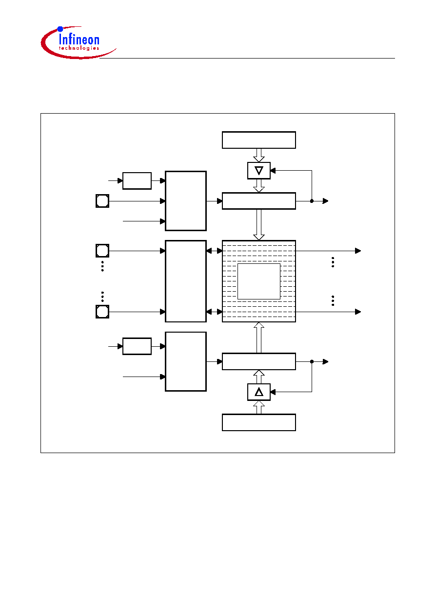
Central Processing Unit (CPU)
The main core of the CPU consists of a 4-stage instruction pipeline, a 16-bit arithmetic
and logic unit (ALU) and dedicated SFRs. Additional hardware has been spent for a
separate multiply and divide unit, a bit-mask generator and a barrel shifter.
Based on these hardware provisions, most of the C161CS/JC/JI's instructions can be
executed in just one machine cycle which requires 80 ns at 25 MHz CPU clock. For
example, shift and rotate instructions are always processed during one machine cycle
independent of the number of bits to be shifted. All multiple-cycle instructions have been
optimized so that they can be executed very fast as well: branches in 2 cycles, a 16
�
16
bit multiplication in 5 cycles and a 32-/16-bit division in 10 cycles. Another pipeline
optimization, the so-called `Jump Cache', allows reducing the execution time of
repeatedly performed jumps in a loop from 2 cycles to 1 cycle.
Figure 4
CPU Block Diagram
MCB02147
CPU
SP
STKOV
STKUN
Instr. Reg.
Instr. Ptr.
Exec. Unit
4-Stage
Pipeline
MDH
MDL
PSW
SYSCON
Context Ptr.
Mul/Div-HW
R15
R0
General
Purpose
Registers
Bit-Mask Gen
Barrel - Shifter
ALU
(16-bit)
Data Page Ptr.
Code Seg. Ptr.
Internal
RAM
R15
R0
ROM
16
16
32
BUSCON 0
BUSCON 1
BUSCON 2
BUSCON 3
BUSCON 4
ADDRSEL 4
ADDRSEL 3
ADDRSEL 2
ADDRSEL 1

C161CS/JC/JI-32R
C161CS/JC/JI-L
Data Sheet
19
V3.0, 2001-01
The CPU has a register context consisting of up to 16 wordwide GPRs at its disposal.
These 16 GPRs are physically allocated within the on-chip RAM area. A Context Pointer
(CP) register determines the base address of the active register bank to be accessed by
the CPU at any time. The number of register banks is only restricted by the available
internal RAM space. For easy parameter passing, a register bank may overlap others.
A system stack of up to 1024 words is provided as a storage for temporary data. The
system stack is allocated in the on-chip RAM area, and it is accessed by the CPU via the
stack pointer (SP) register. Two separate SFRs, STKOV and STKUN, are implicitly
compared against the stack pointer value upon each stack access for the detection of a
stack overflow or underflow.
The high performance offered by the hardware implementation of the CPU can efficiently
be utilized by a programmer via the highly efficient C161CS/JC/JI instruction set which
includes the following instruction classes:
� Arithmetic Instructions
� Logical Instructions
� Boolean Bit Manipulation Instructions
� Compare and Loop Control Instructions
� Shift and Rotate Instructions
� Prioritize Instruction
� Data Movement Instructions
� System Stack Instructions
� Jump and Call Instructions
� Return Instructions
� System Control Instructions
� Miscellaneous Instructions
The basic instruction length is either 2 or 4 bytes. Possible operand types are bits, bytes
and words. A variety of direct, indirect or immediate addressing modes are provided to
specify the required operands.

C161CS/JC/JI-32R
C161CS/JC/JI-L
Data Sheet
20
V3.0, 2001-01
Interrupt System
With an interrupt response time within a range from just 5 to 12 CPU clocks (in case of
internal program execution), the C161CS/JC/JI is capable of reacting very fast to the
occurrence of non-deterministic events.
The architecture of the C161CS/JC/JI supports several mechanisms for fast and flexible
response to service requests that can be generated from various sources internal or
external to the microcontroller. Any of these interrupt requests can be programmed to
being serviced by the Interrupt Controller or by the Peripheral Event Controller (PEC).
In contrast to a standard interrupt service where the current program execution is
suspended and a branch to the interrupt vector table is performed, just one cycle is
`stolen' from the current CPU activity to perform a PEC service. A PEC service implies
a single byte or word data transfer between any two memory locations with an additional
increment of either the PEC source or the destination pointer. An individual PEC transfer
counter is implicity decremented for each PEC service except when performing in the
continuous transfer mode. When this counter reaches zero, a standard interrupt is
performed to the corresponding source related vector location. PEC services are very
well suited, for example, for supporting the transmission or reception of blocks of data.
The C161CS/JC/JI has 8 PEC channels each of which offers such fast interrupt-driven
data transfer capabilities.
A separate control register which contains an interrupt request flag, an interrupt enable
flag and an interrupt priority bitfield exists for each of the possible interrupt sources. Via
its related register, each source can be programmed to one of sixteen interrupt priority
levels. Once having been accepted by the CPU, an interrupt service can only be
interrupted by a higher prioritized service request. For the standard interrupt processing,
each of the possible interrupt sources has a dedicated vector location.
Fast external interrupt inputs are provided to service external interrupts with high
precision requirements. These fast interrupt inputs feature programmable edge
detection (rising edge, falling edge or both edges).
Software interrupts are supported by means of the `TRAP' instruction in combination with
an individual trap (interrupt) number.
Table 3
shows all of the possible C161CS/JC/JI interrupt sources and the corresponding
hardware-related interrupt flags, vectors, vector locations and trap (interrupt) numbers.
Note: Interrupt nodes which are not used by associated peripherals, may be used to
generate software controlled interrupt requests by setting the respective interrupt
request bit (xIR).

C161CS/JC/JI-32R
C161CS/JC/JI-L
Data Sheet
21
V3.0, 2001-01
Table 3
C161CS/JC/JI Interrupt Nodes
Source of Interrupt or
PEC Service Request
Request
Flag
Enable
Flag
Interrupt
Vector
Vector
Location
Trap
Number
CAPCOM Register 0
CC0IR
CC0IE
CC0INT
00'0040
H
10
H
CAPCOM Register 1
CC1IR
CC1IE
CC1INT
00'0044
H
11
H
CAPCOM Register 2
CC2IR
CC2IE
CC2INT
00'0048
H
12
H
CAPCOM Register 3
CC3IR
CC3IE
CC3INT
00'004C
H
13
H
CAPCOM Register 4
CC4IR
CC4IE
CC4INT
00'0050
H
14
H
CAPCOM Register 5
CC5IR
CC5IE
CC5INT
00'0054
H
15
H
CAPCOM Register 6
CC6IR
CC6IE
CC6INT
00'0058
H
16
H
CAPCOM Register 7
CC7IR
CC7IE
CC7INT
00'005C
H
17
H
CAPCOM Register 8
CC8IR
CC8IE
CC8INT
00'0060
H
18
H
CAPCOM Register 9
CC9IR
CC9IE
CC9INT
00'0064
H
19
H
CAPCOM Register 10
CC10IR
CC10IE
CC10INT
00'0068
H
1A
H
CAPCOM Register 11
CC11IR
CC11IE
CC11INT
00'006C
H
1B
H
CAPCOM Register 12
CC12IR
CC12IE
CC12INT
00'0070
H
1C
H
CAPCOM Register 13
CC13IR
CC13IE
CC13INT
00'0074
H
1D
H
CAPCOM Register 14
CC14IR
CC14IE
CC14INT
00'0078
H
1E
H
CAPCOM Register 15
CC15IR
CC15IE
CC15INT
00'007C
H
1F
H
CAPCOM Register 16
CC16IR
CC16IE
CC16INT
00'00C0
H
30
H
CAPCOM Register 17
CC17IR
CC17IE
CC17INT
00'00C4
H
31
H
CAPCOM Register 18
CC18IR
CC18IE
CC18INT
00'00C8
H
32
H
CAPCOM Register 19
CC19IR
CC19IE
CC19INT
00'00CC
H
33
H
CAPCOM Register 20
CC20IR
CC20IE
CC20INT
00'00D0
H
34
H
CAPCOM Register 21
CC21IR
CC21IE
CC21INT
00'00D4
H
35
H
CAPCOM Register 22
CC22IR
CC22IE
CC22INT
00'00D8
H
36
H
CAPCOM Register 23
CC23IR
CC23IE
CC23INT
00'00DC
H
37
H
CAPCOM Register 24
CC24IR
CC24IE
CC24INT
00'00E0
H
38
H
CAPCOM Register 25
CC25IR
CC25IE
CC25INT
00'00E4
H
39
H
CAPCOM Register 26
CC26IR
CC26IE
CC26INT
00'00E8
H
3A
H
CAPCOM Register 27
CC27IR
CC27IE
CC27INT
00'00EC
H
3B
H
CAPCOM Register 28
CC28IR
CC28IE
CC28INT
00'00E0
H
3C
H
CAPCOM Register 29
CC29IR
CC29IE
CC29INT
00'0110
H
44
H
C161CS/JC/JI-32R
C161CS/JC/JI-L
Data Sheet
22
V3.0, 2001-01
CAPCOM Register 30
CC30IR
CC30IE
CC30INT
00'0114
H
45
H
CAPCOM Register 31
CC31IR
CC31IE
CC31INT
00'0118
H
46
H
CAPCOM Timer 0
T0IR
T0IE
T0INT
00'0080
H
20
H
CAPCOM Timer 1
T1IR
T1IE
T1INT
00'0084
H
21
H
CAPCOM Timer 7
T7IR
T7IE
T7INT
00'00F4
H
3D
H
CAPCOM Timer 8
T8IR
T8IE
T8INT
00'00F8
H
3E
H
GPT1 Timer 2
T2IR
T2IE
T2INT
00'0088
H
22
H
GPT1 Timer 3
T3IR
T3IE
T3INT
00'008C
H
23
H
GPT1 Timer 4
T4IR
T4IE
T4INT
00'0090
H
24
H
GPT2 Timer 5
T5IR
T5IE
T5INT
00'0094
H
25
H
GPT2 Timer 6
T6IR
T6IE
T6INT
00'0098
H
26
H
GPT2 CAPREL Reg.
CRIR
CRIE
CRINT
00'009C
H
27
H
A/D Conversion Compl. ADCIR
ADCIE
ADCINT
00'00A0
H
28
H
A/D Overrun Error
ADEIR
ADEIE
ADEINT
00'00A4
H
29
H
ASC0 Transmit
S0TIR
S0TIE
S0TINT
00'00A8
H
2A
H
ASC0 Transmit Buffer
S0TBIR
S0TBIE
S0TBINT
00'011C
H
47
H
ASC0 Receive
S0RIR
S0RIE
S0RINT
00'00AC
H
2B
H
ASC0 Error
S0EIR
S0EIE
S0EINT
00'00B0
H
2C
H
SSC Transmit
SCTIR
SCTIE
SCTINT
00'00B4
H
2D
H
SSC Receive
SCRIR
SCRIE
SCRINT
00'00B8
H
2E
H
SSC Error
SCEIR
SCEIE
SCEINT
00'00BC
H
2F
H
IIC Data Transfer Event XP0IR
XP0IE
XP0INT
00'0100
H
40
H
IIC Protocol Event
XP1IR
XP1IE
XP1INT
00'0104
H
41
H
CAN1 (C161CS/JC)
XP2IR
XP2IE
XP2INT
00'0108
H
42
H
PLL/OWD and RTC
XP3IR
XP3IE
XP3INT
00'010C
H
43
H
ASC1 Transmit
XP4IR
XP4IE
XP4INT
00'0120
H
48
H
ASC1 Receive
XP5IR
XP5IE
XP5INT
00'0124
H
49
H
ASC1 Error
XP6IR
XP6IE
XP6INT
00'0128
H
4A
H
CAN2 (C161CS) or
SDLM (C161JC/JI)
XP7IR
XP7IE
XP7INT
00'012C
H
4B
H
Table 3
C161CS/JC/JI Interrupt Nodes (cont'd)
Source of Interrupt or
PEC Service Request
Request
Flag
Enable
Flag
Interrupt
Vector
Vector
Location
Trap
Number

C161CS/JC/JI-32R
C161CS/JC/JI-L
Data Sheet
23
V3.0, 2001-01
The C161CS/JC/JI also provides an excellent mechanism to identify and to process
exceptions or error conditions that arise during run-time, so-called `Hardware Traps'.
Hardware traps cause immediate non-maskable system reaction which is similar to a
standard interrupt service (branching to a dedicated vector table location). The
occurence of a hardware trap is additionally signified by an individual bit in the trap flag
register (TFR). Except when another higher prioritized trap service is in progress, a
hardware trap will interrupt any actual program execution. In turn, hardware trap services
can normally not be interrupted by standard or PEC interrupts.
Table 4
shows all of the possible exceptions or error conditions that can arise during run-
time:
Table 4
Hardware Trap Summary
Exception Condition
Trap
Flag
Trap
Vector
Vector
Location
Trap
Number
Trap
Priority
Reset Functions:
Hardware Reset
Software Reset
W-dog Timer Overflow
�
RESET
RESET
RESET
00'0000
H
00'0000
H
00'0000
H
00
H
00
H
00
H
III
III
III
Class A Hardware Traps:
Non-Maskable Interrupt
Stack Overflow
Stack Underflow
NMI
STKOF
STKUF
NMITRAP
STOTRAP
STUTRAP
00'0008
H
00'0010
H
00'0018
H
02
H
04
H
06
H
II
II
II
Class B Hardware Traps:
Undefined Opcode
Protected Instruction
Fault
Illegal Word Operand
Access
Illegal Instruction
Access
Illegal External Bus
Access
UNDOPC
PRTFLT
ILLOPA
ILLINA
ILLBUS
BTRAP
BTRAP
BTRAP
BTRAP
BTRAP
00'0028
H
00'0028
H
00'0028
H
00'0028
H
00'0028
H
0A
H
0A
H
0A
H
0A
H
0A
H
I
I
I
I
I
Reserved
�
�
[2C
H
�
3C
H
]
[0B
H
�
0F
H
]
�
Software Traps
TRAP Instruction
�
�
Any
[00'0000
H
�
00'01FC
H
]
in steps
of 4
H
Any
[00
H
�
7F
H
]
Current
CPU
Priority

C161CS/JC/JI-32R
C161CS/JC/JI-L
Data Sheet
24
V3.0, 2001-01
Capture/Compare (CAPCOM) Units
The CAPCOM units support generation and control of timing sequences on up to
32 channels with a maximum resolution of 16 TCL. The CAPCOM units are typically
used to handle high speed I/O tasks such as pulse and waveform generation, pulse
width modulation (PMW), Digital to Analog (D/A) conversion, software timing, or time
recording relative to external events.
Four 16-bit timers (T0/T1, T7/T8) with reload registers provide two independent time
bases for the capture/compare register array.
The input clock for the timers is programmable to several prescaled values of the internal
system clock, or may be derived from an overflow/underflow of timer T6 in module
GPT2. This provides a wide range of variation for the timer period and resolution and
allows precise adjustments to the application specific requirements. In addition, external
count inputs for CAPCOM timers T0 and T7 allow event scheduling for the capture/
compare registers relative to external events.
Both of the two capture/compare register arrays contain 16 dual purpose capture/
compare registers, each of which may be individually allocated to either CAPCOM timer
T0 or T1 (T7 or T8, respectively), and programmed for capture or compare function.
Eight registers of each module have one port pin associated with it which serves as an
input pin for triggering the capture function, or as an output pin to indicate the occurrence
of a compare event.
When a capture/compare register has been selected for capture mode, the current
contents of the allocated timer will be latched (`captured') into the capture/compare
register in response to an external event at the port pin which is associated with this
register. In addition, a specific interrupt request for this capture/compare register is
generated. Either a positive, a negative, or both a positive and a negative external signal
transition at the pin can be selected as the triggering event.
The contents of all registers which have been selected for one of the five compare
modes are continuously compared with the contents of the allocated timers.
Table 5
Compare Modes (CAPCOM)
Compare Modes
Function
Mode 0
Interrupt-only compare mode;
several compare interrupts per timer period are possible
Mode 1
Pin toggles on each compare match;
several compare events per timer period are possible
Mode 2
Interrupt-only compare mode;
only one compare interrupt per timer period is generated
Mode 3
Pin set `1' on match; pin reset `0' on compare time overflow;
only one compare event per timer period is generated
C161CS/JC/JI-32R
C161CS/JC/JI-L
Data Sheet
25
V3.0, 2001-01
When a match occurs between the timer value and the value in a capture/compare
register, specific actions will be taken based on the selected compare mode.
Figure 5
CAPCOM Unit Block Diagram
MCB02143c
Mode
Control
(Capture
or
Compare)
2
n
: 1
f
CPU
Tx
Input
Control
CAPCOM Timer Tx
Ty
Input
Control
TxIN
Interrupt
Request
GPT2 Timer T6
Over/Underflow
2
n
: 1
f
CPU
GPT2 Timer T6
Over/Underflow
CCxIO
CCxIO
8 Capture Inputs
8 Compare Outputs
Reload Reg. TxREL
CAPCOM Timer Ty
Reload Reg. TyREL
Interrupt
Request
16 Capture/Compare
Interrupt Request
16-Bit
Capture/
Compare
Registers
x = 0, 7
y = 1, 8
n = 3 ... 10

C161CS/JC/JI-32R
C161CS/JC/JI-L
Data Sheet
26
V3.0, 2001-01
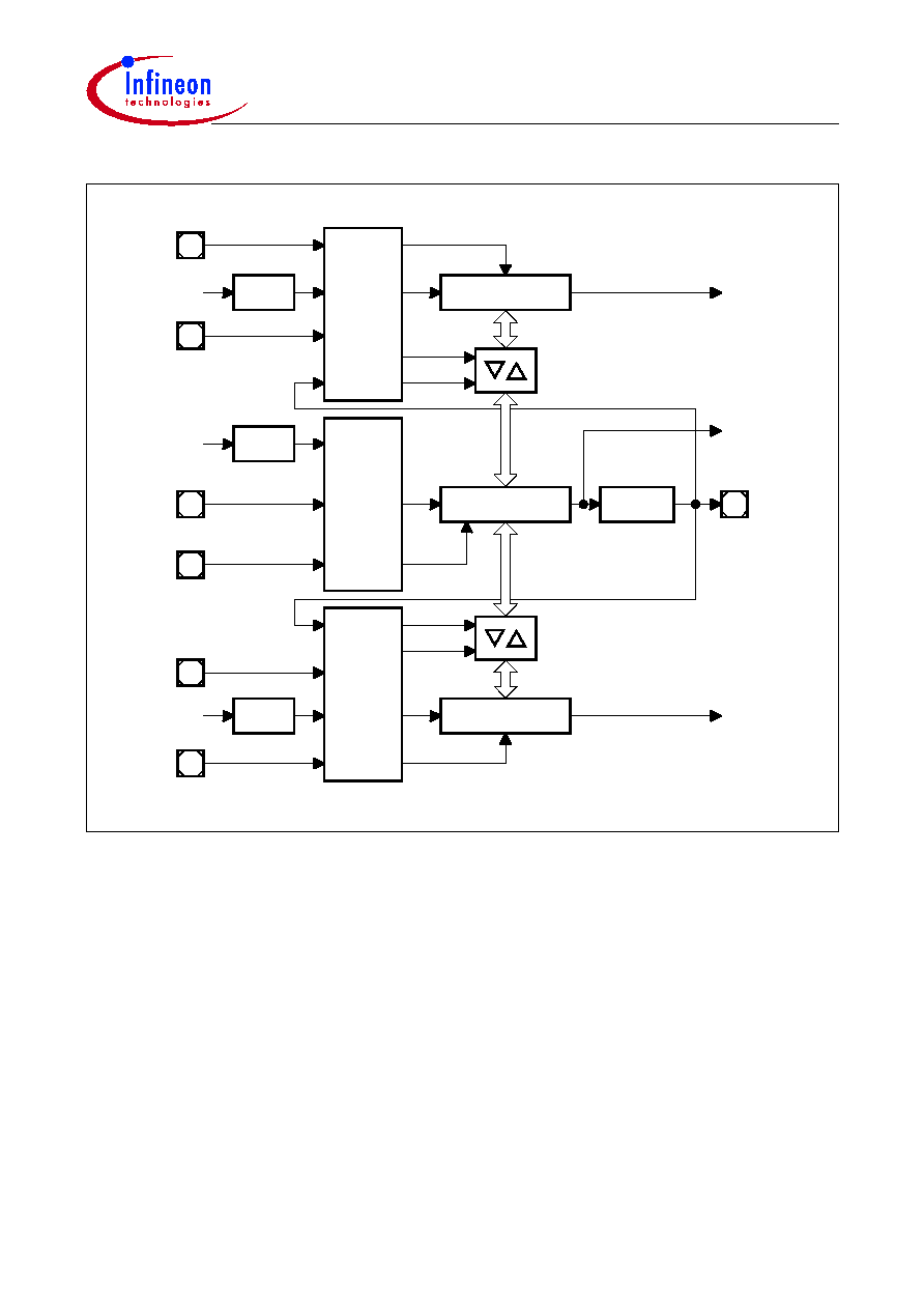
General Purpose Timer (GPT) Unit
The GPT unit represents a very flexible multifunctional timer/counter structure which
may be used for many different time related tasks such as event timing and counting,
pulse width and duty cycle measurements, pulse generation, or pulse multiplication.
The GPT unit incorporates five 16-bit timers which are organized in two separate
modules, GPT1 and GPT2. Each timer in each module may operate independently in a
number of different modes, or may be concatenated with another timer of the same
module.
Each of the three timers T2, T3, T4 of module GPT1 can be configured individually for
one of four basic modes of operation, which are Timer, Gated Timer, Counter, and
Incremental Interface Mode. In Timer Mode, the input clock for a timer is derived from
the CPU clock, divided by a programmable prescaler, while Counter Mode allows a timer
to be clocked in reference to external events.
Pulse width or duty cycle measurement is supported in Gated Timer Mode, where the
operation of a timer is controlled by the `gate' level on an external input pin. For these
purposes, each timer has one associated port pin (TxIN) which serves as gate or clock
input. The maximum resolution of the timers in module GPT1 is 16 TCL.
The count direction (up/down) for each timer is programmable by software or may
additionally be altered dynamically by an external signal on a port pin (TxEUD) to
facilitate e.g. position tracking.
In Incremental Interface Mode the GPT1 timers (T2, T3, T4) can be directly connected
to the incremental position sensor signals A and B via their respective inputs TxIN and
TxEUD. Direction and count signals are internally derived from these two input signals,
so the contents of the respective timer Tx corresponds to the sensor position. The third
position sensor signal TOP0 can be connected to an interrupt input.
Timer T3 has an output toggle latch (T3OTL) which changes its state on each timer over-
flow/underflow. The state of this latch may be output on pin T3OUT e.g. for time out
monitoring of external hardware components, or may be used internally to clock timers
T2 and T4 for measuring long time periods with high resolution.
In addition to their basic operating modes, timers T2 and T4 may be configured as reload
or capture registers for timer T3. When used as capture or reload registers, timers T2
and T4 are stopped. The contents of timer T3 is captured into T2 or T4 in response to a
signal at their associated input pins (TxIN). Timer T3 is reloaded with the contents of T2
or T4 triggered either by an external signal or by a selectable state transition of its toggle
latch T3OTL. When both T2 and T4 are configured to alternately reload T3 on opposite
state transitions of T3OTL with the low and high times of a PWM signal, this signal can
be constantly generated without software intervention.
C161CS/JC/JI-32R
C161CS/JC/JI-L
Data Sheet
27
V3.0, 2001-01
Figure 6
Block Diagram of GPT1
With its maximum resolution of 8 TCL, the GPT2 module provides precise event control
and time measurement. It includes two timers (T5, T6) and a capture/reload register
(CAPREL). Both timers can be clocked with an input clock which is derived from the CPU
clock via a programmable prescaler or with external signals. The count direction (up/
down) for each timer is programmable by software or may additionally be altered
dynamically by an external signal on a port pin (TxEUD). Concatenation of the timers is
supported via the output toggle latch (T6OTL) of timer T6, which changes its state on
each timer overflow/underflow.
The state of this latch may be used to clock timer T5, and/or it may be output on pin
T6OUT. The overflows/underflows of timer T6 can additionally be used to clock the
CAPCOM timers T0 or T1, and to cause a reload from the CAPREL register. The
CAPREL register may capture the contents of timer T5 based on an external signal
transition on the corresponding port pin (CAPIN), and timer T5 may optionally be cleared
T3
Mode
Control
2
n
: 1
f
CPU
2
n
: 1
f
CPU
T2
Mode
Control
GPT1 Timer T2
Reload
Capture
2
n
: 1
f
CPU
T4
Mode
Control
GPT1 Timer T4
Reload
Capture
GPT1 Timer T3
T3OTL
U/D
T2EUD
T2IN
T3IN
T3EUD
T4IN
T4EUD
T3OUT
Toggle FF
U/D
U/D
Interrupt
Request
(T2IR)
Interrupt
Request
(T3IR)
Interrupt
Request
(T4IR)
MCT04825
n = 3 ... 10
C161CS/JC/JI-32R
C161CS/JC/JI-L
Data Sheet
28
V3.0, 2001-01
after the capture procedure. This allows the C161CS/JC/JI to measure absolute time
differences or to perform pulse multiplication without software overhead.
The capture trigger (timer T5 to CAPREL) may also be generated upon transitions of
GPT1 timer T3's inputs T3IN and/or T3EUD. This is especially advantageous when T3
operates in Incremental Interface Mode.
Figure 7
Block Diagram of GPT2
n = 2 ... 9
MUX
2
n
: 1
f
CPU
T5
Mode
Control
GPT2 Timer T5
2
n
: 1
f
CPU
T6
Mode
Control
GPT2 Timer T6
GPT2 CAPREL
T6OTL
T5IN
T3
CAPIN
T6IN
T6OUT
U/D
U/D
Interrupt
Request
(T5IR)
Interrupt
Request
(CRIR)
Interrupt
Request
(T6IR)
To auxiliary
Timers
Clear
Capture
CT3
mcb03999b.vsd
To other
Modules
C161CS/JC/JI-32R
C161CS/JC/JI-L
Data Sheet
29
V3.0, 2001-01
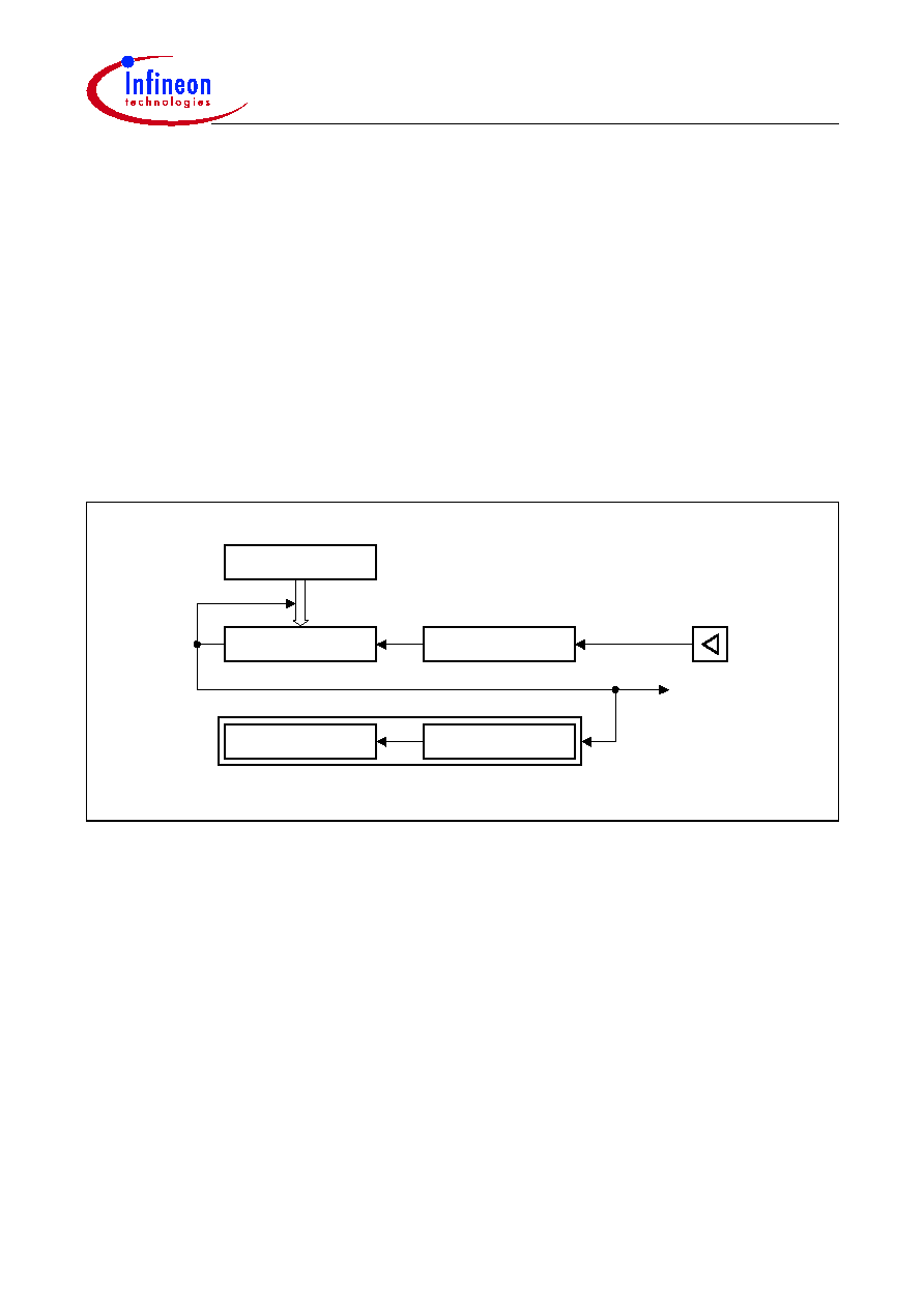
Real Time Clock
The Real Time Clock (RTC) module of the C161CS/JC/JI consists of a chain of 3 divider
blocks, a fixed 8:1 divider, the reloadable 16-bit timer T14, and the 32-bit RTC timer
(accessible via registers RTCH and RTCL). The RTC module is directly clocked via a
separate clock driver with the on-chip main oscillator frequency divided by 32
(
f
RTC
=
f
OSCm
/ 32) or with the on-chip auxiliary oscillator frequency (
f
RTC
=
f
OSCa
). It is
therefore independent from the selected clock generation mode of the C161CS/JC/JI.
All timers count up.
The RTC module can be used for different purposes:
� System clock to determine the current time and date
� Cyclic time based interrupt
� 48-bit timer for long term measurements
Figure 8
RTC Block Diagram
Note: The registers associated with the RTC are not affected by a reset in order to
maintain the correct system time even when intermediate resets are executed.
MCD04432
T14REL
T14
8:1
RTC
f
RTCL
RTCH
Interrupt
Request
Reload

C161CS/JC/JI-32R
C161CS/JC/JI-L
Data Sheet
30
V3.0, 2001-01
A/D Converter
For analog signal measurement, a 10-bit A/D converter with 12 multiplexed input
channels and a sample and hold circuit has been integrated on-chip. It uses the method
of successive approximation. The sample time (for loading the capacitors) and the
conversion time is programmable and can so be adjusted to the external circuitry.
Overrun error detection/protection is provided for the conversion result register
(ADDAT): either an interrupt request will be generated when the result of a previous
conversion has not been read from the result register at the time the next conversion is
complete, or the next conversion is suspended in such a case until the previous result
has been read.
For applications which require less than 12 analog input channels, the remaining
channel inputs can be used as digital input port pins.
The A/D converter of the C161CS/JC/JI supports four different conversion modes. In the
standard Single Channel conversion mode, the analog level on a specified channel is
sampled once and converted to a digital result. In the Single Channel Continuous mode,
the analog level on a specified channel is repeatedly sampled and converted without
software intervention. In the Auto Scan mode, the analog levels on a prespecified
number of channels (standard or extension) are sequentially sampled and converted. In
the Auto Scan Continuous mode, the number of prespecified channels is repeatedly
sampled and converted. In addition, the conversion of a specific channel can be inserted
(injected) into a running sequence without disturbing this sequence. This is called
Channel Injection Mode.
The Peripheral Event Controller (PEC) may be used to automatically store the
conversion results into a table in memory for later evaluation, without requiring the
overhead of entering and exiting interrupt routines for each data transfer.
After each reset and also during normal operation the ADC automatically performs
calibration cycles. This automatic self-calibration constantly adjusts the converter to
changing operating conditions (e.g. temperature) and compensates process variations.
These calibration cycles are part of the conversion cycle, so they do not affect the normal
operation of the A/D converter.
In order to decouple analog inputs from digital noise and to avoid input trigger noise
those pins used for analog input can be disconnected from the digital IO or input stages
under software control. This can be selected for each pin separately via register
P5DIDIS (Port 5 Digital Input Disable).

C161CS/JC/JI-32R
C161CS/JC/JI-L
Data Sheet
31
V3.0, 2001-01
Serial Channels
Serial communication with other microcontrollers, processors, terminals or external
peripheral components is provided by three serial interfaces with different functionality,
two Asynchronous/Synchronous Serial Channels (ASC0/ASC1) and a High-Speed
Synchronous Serial Channel (SSC).
The ASC0 is upward compatible with the serial ports of the Infineon 8-bit microcontroller
families and supports full-duplex asynchronous communication at up to 781 kBaud and
half-duplex synchronous communication at up to 3.1 MBaud (@ 25 MHz CPU clock).
A dedicated baud rate generator allows to set up all standard baud rates without
oscillator tuning. For transmission, reception and error handling 4 separate interrupt
vectors are provided. In asynchronous mode, 8- or 9-bit data frames are transmitted or
received, preceded by a start bit and terminated by one or two stop bits. For
multiprocessor communication, a mechanism to distinguish address from data bytes has
been included (8-bit data plus wake up bit mode).
In synchronous mode, the ASC0 transmits or receives bytes (8 bits) synchronously to a
shift clock which is generated by the ASC0. The ASC0 always shifts the LSB first. A loop
back option is available for testing purposes.
A number of optional hardware error detection capabilities has been included to increase
the reliability of data transfers. A parity bit can automatically be generated on
transmission or be checked on reception. Framing error detection allows to recognize
data frames with missing stop bits. An overrun error will be generated, if the last
character received has not been read out of the receive buffer register at the time the
reception of a new character is complete.
The ASC1 is function compatible with the ASC0, except that its registers are not bit-
addressable (XBUS peripheral) and it provides only three interrupt vectors.
The SSC supports full-duplex synchronous communication at up to 6.25 MBaud
(@ 25 MHz CPU clock). It may be configured so it interfaces with serially linked
peripheral components. A dedicated baud rate generator allows to set up all standard
baud rates without oscillator tuning. For transmission, reception and error handling three
separate interrupt vectors are provided.
The SSC transmits or receives characters of 2 ... 16 bits length synchronously to a shift
clock which can be generated by the SSC (master mode) or by an external master (slave
mode). The SSC can start shifting with the LSB or with the MSB and allows the selection
of shifting and latching clock edges as well as the clock polarity.
A number of optional hardware error detection capabilities has been included to increase
the reliability of data transfers. Transmit and receive error supervise the correct handling
of the data buffer. Phase and baudrate error detect incorrect serial data.

C161CS/JC/JI-32R
C161CS/JC/JI-L
Data Sheet
32
V3.0, 2001-01
Serial Data Link Module (SDLM)
The Serial Data Link Module (SDLM) provides serial communication via a J1850 type
multiplexed serial bus via an external J1850 bus transceiver. The module conforms to
the SAE Class B J1850 specification for variable pulse width modulation (VPW). The
SDLM is integrated as an on-chip peripheral and is connected to the CPU via the XBUS.
General SDLM Features:
� Compliant to the SAE Class B J1850 specification (VPW)
� Class 2 protocol fully supported
� Variable Pulse Width (VPW) operation at 10.4 kBaud
� High Speed 4X operation at 41.6 kBaud
� Programmable Normalization Bit
� Programmable Delay for transceiver interface
� Digital Noise Filter
� Power Down mode with automatic wakeup support upon bus activity
� Single Byte Header and Consolidated Header supported
� CRC generation and checking
� Receive and transmit Block Mode
Data Link Operation Features:
� 11 Byte Transmit Buffer
� Double buffered 11 Byte receive buffer (optional overwrite enable)
� Support for In Frame Response (IFR) types 1, 2 and 3
� Transmit and Receiver Message Buffers configurable for either FIFO or Byte mode
� Advanced Interrupt Handling with 8 separately enabled sources:
Error, format or bus shorted
CRC error
Lost Arbitration
Break received
In-Frame-Response request
Header received
Complete message received
Transmit successful
� Automatic IFR transmission (Types 1 and 2) for 3-Byte consolidated headers
� User configurable clock divider
� Bus status flags (IDLE, EOF, EOD, SOF, Tx and Rx in progress)
Note: When the SDLM is used with the interface lines assigned to Port 4, the interface
lines override the segment address lines and the segment address output on
Port 4 is therefore limited to 6/4 bits i.e. address lines A21/A19 ... A16. CS lines
can be used to increase the total amount of addressable external memory.

C161CS/JC/JI-32R
C161CS/JC/JI-L
Data Sheet
33
V3.0, 2001-01
CAN-Modules
The integrated CAN-Modules handle the completely autonomous transmission and
reception of CAN frames in accordance with the CAN specification V2.0 part B (active),
i.e. the on-chip CAN-Modules can receive and transmit standard frames with 11-bit
identifiers as well as extended frames with 29-bit identifiers.
The modules provide Full CAN functionality on up to 15 message objects each.
Message object 15 may be configured for Basic CAN functionality. Both modes provide
separate masks for acceptance filtering which allows to accept a number of identifiers in
Full CAN mode and also allows to disregard a number of identifiers in Basic CAN mode.
All message objects can be updated independent from the other objects and are
equipped for the maximum message length of 8 bytes.
The bit timing is derived from the XCLK and is programmable up to a data rate of
1 MBaud. Each CAN-Module uses two pins of Port 4 or Port 8 to interface to an external
bus transceiver. The interface pins are assigned via software.
Module CAN2 (C161CS only) is identical with the first one, except that it uses a separate
address area and a separate interrupt node.
The two CAN modules can be internally coupled by assigning their interface pins to the
same two port pins, or they can interface to separate CAN buses.
Note: When one or both of the on-chip CAN Modules are used with the interface lines
assigned to Port 4, the interface lines override the segment address lines and the
segment address output on Port 4 is therefore limited to 6/4 bits i.e. address lines
A21/A19 ... A16. CS lines can be used to increase the total amount of addressable
external memory.
IIC Module
The integrated IIC Bus Module handles the transmission and reception of frames over
the two-line IIC bus in accordance with the IIC Bus specification. The on-chip IIC Module
can receive and transmit data using 7-bit or 10-bit addressing and it can operate in slave
mode, in master mode or in multi-master mode.
Several physical interfaces (port pins) can be established under software control. Data
can be transferred at speeds up to 400 kbit/sec.
Two interrupt nodes dedicated to the IIC module allow efficient interrupt service and also
support operation via PEC transfers.
Note: The port pins associated with the IIC interfaces feature open drain drivers only, as
required by the IIC specification.

C161CS/JC/JI-32R
C161CS/JC/JI-L
Data Sheet
34
V3.0, 2001-01
Parallel Ports
The C161CS/JC/JI provides up to 93 I/O lines which are organized into eight input/output
ports and one input port. All port lines are bit-addressable, and all input/output lines are
individually (bit-wise) programmable as inputs or outputs via direction registers. The I/O
ports are true bidirectional ports which are switched to high impedance state when
configured as inputs. The output drivers of five I/O ports can be configured (pin by pin)
for push/pull operation or open-drain operation via control registers, Port 9 provides
open-drain-only drivers. During the internal reset, all port pins are configured as inputs.
The input threshold of Port 2, Port 3, Port 4, Port 6, and Port 7 is selectable (TTL or
CMOS like), where the special CMOS like input threshold reduces noise sensitivity due
to the input hysteresis. The input threshold may be selected individually for each byte of
the respective ports.
All port lines have programmable alternate input or output functions associated with
them. All port lines that are not used for these alternate functions may be used as
general purpose IO lines.
PORT0 and PORT1 may be used as address and data lines when accessing external
memory, while Port 4 outputs the additional segment address bits A23/19/17 ... A16 in
systems where segmentation is enabled to access more than 64 KBytes of memory.
Port 2, Port 7, and parts of PORT1 are associated with the capture inputs or compare
outputs of the CAPCOM units.
Port 6 provides optional bus arbitration signals (BREQ, HLDA, HOLD) and chip select
signals.
Port 3 includes alternate functions of timers, serial interfaces, the optional bus control
signal BHE, and the system clock output CLKOUT (or the programmable frequency
output FOUT).
Port 5 is used for the analog input channels to the A/D converter or timer control signals.
The edge characteristics (transition time) and driver characteristics (output current) of
the C161CS/JC/JI's port drivers can be selected via the Port Output Control registers
(POCONx).

C161CS/JC/JI-32R
C161CS/JC/JI-L
Data Sheet
35
V3.0, 2001-01
Watchdog Timer
The Watchdog Timer represents one of the fail-safe mechanisms which have been
implemented to prevent the controller from malfunctioning for longer periods of time.
The Watchdog Timer is always enabled after a reset of the chip, and can only be
disabled in the time interval until the EINIT (end of initialization) instruction has been
executed. Thus, the chip's start-up procedure is always monitored. The software has to
be designed to service the Watchdog Timer before it overflows. If, due to hardware or
software related failures, the software fails to do so, the Watchdog Timer overflows and
generates an internal hardware reset and pulls the RSTOUT pin low in order to allow
external hardware components to be reset.
The Watchdog Timer is a 16-bit timer, clocked with the system clock divided by 2/4/128/
256. The high byte of the Watchdog Timer register can be set to a prespecified reload
value (stored in WDTREL) in order to allow further variation of the monitored time
interval. Each time it is serviced by the application software, the high byte of the
Watchdog Timer is reloaded. Thus, time intervals between 20
�
s and 671 ms can be
monitored (@ 25 MHz).
The default Watchdog Timer interval after reset is 5.24 ms (@ 25 MHz).
Oscillator Watchdog
The Oscillator Watchdog (OWD) monitors the clock signal generated by the on-chip
oscillator (either with a crystal or via external clock drive). For this operation the PLL
provides a clock signal which is used to supervise transitions on the oscillator clock. This
PLL clock is independent from the XTAL1 clock. When the expected oscillator clock
transitions are missing the OWD activates the PLL Unlock / OWD interrupt node and
supplies the CPU with the PLL clock signal. Under these circumstances the PLL will
oscillate with its basic frequency.
In direct drive mode the PLL base frequency is used directly (
f
CPU
= 2 ... 5 MHz).
In prescaler mode the PLL base frequency is divided by 2 (
f
CPU
= 1 ... 2.5 MHz).
Note: The CPU clock source is only switched back to the oscillator clock after a
hardware reset.
The oscillator watchdog can be disabled by setting bit OWDDIS in register SYSCON.
In this case (OWDDIS = `1') the PLL remains idle and provides no clock signal, while the
CPU clock signal is derived directly from the oscillator clock or via prescaler or SDD. Also
no interrupt request will be generated in case of a missing oscillator clock.
Note: At the end of an external reset (EA = `0') bit OWDDIS reflects the inverted level of
pin RD at that time. Thus the oscillator watchdog may also be disabled via
hardware by (externally) pulling the RD line low upon a reset, similar to the
standard reset configuration via PORT0. At the end of an internal reset (EA = `1')
bit OWDDIS is cleared.

C161CS/JC/JI-32R
C161CS/JC/JI-L
Data Sheet
36
V3.0, 2001-01
Power Management
The C161CS/JC/JI provides several means to control the power it consumes either at a
given time or averaged over a certain timespan. Three mechanisms can be used (partly
in parallel):
� Power Saving Modes switch the C161CS/JC/JI into a special operating mode
(control via instructions).
Idle Mode stops the CPU while the peripherals can continue to operate.
Sleep Mode and Power Down Mode stop all clock signals and all operation (RTC may
optionally continue running). Sleep Mode can be terminated by external interrupt
signals.
� Clock Generation Management controls the distribution and the frequency of
internal and external clock signals (control via register SYSCON2).
Slow Down Mode lets the C161CS/JC/JI run at a CPU clock frequency of
f
OSC
/
1 ... 32 (half for prescaler operation) which drastically reduces the consumed power.
The PLL can be optionally disabled while operating in Slow Down Mode.
External circuitry can be controlled via the programmable frequency output FOUT.
� Peripheral Management permits temporary disabling of peripheral modules (control
via register SYSCON3).
Each peripheral can separately be disabled/enabled. A group control option disables
a major part of the peripheral set by setting one single bit.
The on-chip RTC supports intermittend operation of the C161CS/JC/JI by generating
cyclic wakeup signals. This offers full performance to quickly react on action requests
while the intermittend sleep phases greatly reduce the average power consumption of
the system.
C161CS/JC/JI-32R
C161CS/JC/JI-L
Data Sheet
37
V3.0, 2001-01
Instruction Set Summary
Table 6
lists the instructions of the C161CS/JC/JI in a condensed way.
The various addressing modes that can be used with a specific instruction, the operation
of the instructions, parameters for conditional execution of instructions, and the opcodes
for each instruction can be found in the "C166 Family Instruction Set Manual".
This document also provides a detailled description of each instruction.
Table 6
Instruction Set Summary
Mnemonic
Description
Bytes
ADD(B)
Add word (byte) operands
2 / 4
ADDC(B)
Add word (byte) operands with Carry
2 / 4
SUB(B)
Subtract word (byte) operands
2 / 4
SUBC(B)
Subtract word (byte) operands with Carry
2 / 4
MUL(U)
(Un)Signed multiply direct GPR by direct GPR (16-16-bit) 2
DIV(U)
(Un)Signed divide register MDL by direct GPR (16-/16-bit) 2
DIVL(U)
(Un)Signed long divide reg. MD by direct GPR (32-/16-bit) 2
CPL(B)
Complement direct word (byte) GPR
2
NEG(B)
Negate direct word (byte) GPR
2
AND(B)
Bitwise AND, (word/byte operands)
2 / 4
OR(B)
Bitwise OR, (word/byte operands)
2 / 4
XOR(B)
Bitwise XOR, (word/byte operands)
2 / 4
BCLR
Clear direct bit
2
BSET
Set direct bit
2
BMOV(N)
Move (negated) direct bit to direct bit
4
BAND, BOR,
BXOR
AND/OR/XOR direct bit with direct bit
4
BCMP
Compare direct bit to direct bit
4
BFLDH/L
Bitwise modify masked high/low byte of bit-addressable
direct word memory with immediate data
4
CMP(B)
Compare word (byte) operands
2 / 4
CMPD1/2
Compare word data to GPR and decrement GPR by 1/2
2 / 4
CMPI1/2
Compare word data to GPR and increment GPR by 1/2
2 / 4
PRIOR
Determine number of shift cycles to normalize direct
word GPR and store result in direct word GPR
2
SHL / SHR
Shift left/right direct word GPR
2
ROL / ROR
Rotate left/right direct word GPR
2
ASHR
Arithmetic (sign bit) shift right direct word GPR
2

C161CS/JC/JI-32R
C161CS/JC/JI-L
Data Sheet
38
V3.0, 2001-01
MOV(B)
Move word (byte) data
2 / 4
MOVBS
Move byte operand to word operand with sign extension
2 / 4
MOVBZ
Move byte operand to word operand. with zero extension 2 / 4
JMPA, JMPI,
JMPR
Jump absolute/indirect/relative if condition is met
4
JMPS
Jump absolute to a code segment
4
J(N)B
Jump relative if direct bit is (not) set
4
JBC
Jump relative and clear bit if direct bit is set
4
JNBS
Jump relative and set bit if direct bit is not set
4
CALLA, CALLI,
CALLR
Call absolute/indirect/relative subroutine if condition is met 4
CALLS
Call absolute subroutine in any code segment
4
PCALL
Push direct word register onto system stack and call
absolute subroutine
4
TRAP
Call interrupt service routine via immediate trap number
2
PUSH, POP
Push/pop direct word register onto/from system stack
2
SCXT
Push direct word register onto system stack and update
register with word operand
4
RET
Return from intra-segment subroutine
2
RETS
Return from inter-segment subroutine
2
RETP
Return from intra-segment subroutine and pop direct
word register from system stack
2
RETI
Return from interrupt service subroutine
2
SRST
Software Reset
4
IDLE
Enter Idle Mode
4
PWRDN
Enter Power Down Mode (supposes NMI-pin being low)
4
SRVWDT
Service Watchdog Timer
4
DISWDT
Disable Watchdog Timer
4
EINIT
Signify End-of-Initialization on RSTOUT-pin
4
ATOMIC
Begin ATOMIC sequence
2
EXTR
Begin EXTended Register sequence
2
EXTP(R)
Begin EXTended Page (and Register) sequence
2 / 4
EXTS(R)
Begin EXTended Segment (and Register) sequence
2 / 4
NOP
Null operation
2
Table 6
Instruction Set Summary (cont'd)
Mnemonic
Description
Bytes

C161CS/JC/JI-32R
C161CS/JC/JI-L
Data Sheet
39
V3.0, 2001-01
Special Function Registers Overview
Table 7
lists all SFRs which are implemented in the C161CS/JC/JI in alphabetical order.
Bit-addressable SFRs are marked with the letter "b" in column "Name". SFRs within the
Extended SFR-Space (ESFRs) are marked with the letter "E" in column "Physical
Address". Registers within on-chip X-peripherals are marked with the letter "X" in column
"Physical Address".
An SFR can be specified via its individual mnemonic name. Depending on the selected
addressing mode, an SFR can be accessed via its physical address (using the Data
Page Pointers), or via its short 8-bit address (without using the Data Page Pointers).
Note: Registers within device specific interface modules (CAN, SDLM) are only present
in the corresponding device, of course.
Table 7
C161CS/JC/JI Registers, Ordered by Name
Name
Physical
Address
8-Bit
Addr.
Description
Reset
Value
ADCIC
b FF98
H
CC
H
A/D Converter End of Conversion
Interrupt Control Register
0000
H
ADCON
b FFA0
H
D0
H
A/D Converter Control Register
0000
H
ADDAT
FEA0
H
50
H
A/D Converter Result Register
0000
H
ADDAT2
F0A0
H
E 50
H
A/D Converter 2 Result Register
0000
H
ADDRSEL1
FE18
H
0C
H
Address Select Register 1
0000
H
ADDRSEL2
FE1A
H
0D
H
Address Select Register 2
0000
H
ADDRSEL3
FE1C
H
0E
H
Address Select Register 3
0000
H
ADDRSEL4
FE1E
H
0F
H
Address Select Register 4
0000
H
ADEIC
b FF9A
H
CD
H
A/D Converter Overrun Error Interrupt
Control Register
0000
H
BUFFCON
EB24
H
X ---
SDLM Buffer Control Register
0000
H
BUFFSTAT
EB1C
H
X ---
SDLM Buffer Status Register
0000
H
BUSCON0 b FF0C
H
86
H
Bus Configuration Register 0
0000
H
BUSCON1 b FF14
H
8A
H
Bus Configuration Register 1
0000
H
BUSCON2 b FF16
H
8B
H
Bus Configuration Register 2
0000
H
BUSCON3 b FF18
H
8C
H
Bus Configuration Register 3
0000
H
BUSCON4 b FF1A
H
8D
H
Bus Configuration Register 4
0000
H
BUSSTAT
EB20
H
X ---
SDLM Bus Status Register
0000
H
C1BTR
EF04
H
X ---
CAN1 Bit Timing Register
UUUU
H
C1CSR
EF00
H
X ---
CAN1 Control / Status Register
XX01
H
C1GMS
EF06
H
X ---
CAN1 Global Mask Short
UFUU
H

C161CS/JC/JI-32R
C161CS/JC/JI-L
Data Sheet
40
V3.0, 2001-01
C1PCIR
EF02
H
X ---
CAN1 Port Control / Interrupt Register
XXXX
H
C1LARn
EFn4
H
X ---
CAN1 Lower Arbitration Reg. (msg. n)
UUUU
H
C1LGML
EF0A
H
X ---
CAN1 Lower Global Mask Long
UUUU
H
C1LMLM
EF0E
H
X ---
CAN1 Lower Mask of Last Message
UUUU
H
C1MCFGn
EFn6
H
X ---
CAN1 Message Config. Reg. (msg. n)
UU
H
C1MCRn
EFn0
H
X ---
CAN1 Message Control Reg. (msg. n)
UUUU
H
C1UARn
EFn2
H
X ---
CAN1 Upper Arbitration Reg. (msg. n)
UUUU
H
C1UGML
EF08
H
X ---
CAN1 Upper Global Mask Long
UUUU
H
C1UMLM
EF0C
H
X ---
CAN1 Upper Mask of Last Message
UUUU
H
C2BTR
EE04
H
X ---
CAN2 Bit Timing Register
UUUU
H
C2CSR
EE00
H
X ---
CAN2 Control / Status Register
XX01
H
C2GMS
EE06
H
X ---
CAN2 Global Mask Short
UFUU
H
C2PCIR
EE02
H
X ---
CAN2 Port Control / Interrupt Register
XXXX
H
C2LARn
EEn4
H
X ---
CAN2 Lower Arbitration Reg. (msg. n)
UUUU
H
C2LGML
EE0A
H
X ---
CAN2 Lower Global Mask Long
UUUU
H
C2LMLM
EE0E
H
X ---
CAN2 Lower Mask of Last Message
UUUU
H
C2MCFGn
EEn6
H
X ---
CAN2 Message Config. Reg. (msg. n)
UU
H
C2MCRn
EEn0
H
X ---
CAN2 Message Control Reg. (msg. n)
UUUU
H
C2UARn
EEn2
H
X ---
CAN2 Upper Arbitration Reg. (msg. n)
UUUU
H
C2UGML
EE08
H
X ---
CAN2 Upper Global Mask Long
UUUU
H
C2UMLM
EE0C
H
X ---
CAN2 Upper Mask of Last Message
UUUU
H
CAPREL
FE4A
H
25
H
GPT2 Capture/Reload Register
0000
H
CC0
FE80
H
40
H
CAPCOM Register 0
0000
H
CC0IC
b FF78
H
BC
H
CAPCOM Register 0 Interrupt Ctrl. Reg.
0000
H
CC1
FE82
H
41
H
CAPCOM Register 1
0000
H
CC10
FE94
H
4A
H
CAPCOM Register 10
0000
H
CC10IC
b FF8C
H
C6
H
CAPCOM Reg. 10 Interrupt Ctrl. Reg.
0000
H
CC11
FE96
H
4B
H
CAPCOM Register 11
0000
H
CC11IC
b FF8E
H
C7
H
CAPCOM Reg. 11 Interrupt Ctrl. Reg.
0000
H
CC12
FE98
H
4C
H
CAPCOM Register 12
0000
H
CC12IC
b FF90
H
C8
H
CAPCOM Reg. 12 Interrupt Ctrl. Reg.
0000
H
CC13
FE9A
H
4D
H
CAPCOM Register 13
0000
H
Table 7
C161CS/JC/JI Registers, Ordered by Name (cont'd)
Name
Physical
Address
8-Bit
Addr.
Description
Reset
Value
C161CS/JC/JI-32R
C161CS/JC/JI-L
Data Sheet
41
V3.0, 2001-01
CC13IC
b FF92
H
C9
H
CAPCOM Reg. 13 Interrupt Ctrl. Reg.
0000
H
CC14
FE9C
H
4E
H
CAPCOM Register 14
0000
H
CC14IC
b FF94
H
CA
H
CAPCOM Reg. 14 Interrupt Ctrl. Reg.
0000
H
CC15
FE9E
H
4F
H
CAPCOM Register 15
0000
H
CC15IC
b FF96
H
CB
H
CAPCOM Reg. 15 Interrupt Ctrl. Reg.
0000
H
CC16
FE60
H
30
H
CAPCOM Register 16
0000
H
CC16IC
b F160
H
E B0
H
CAPCOM Reg.16 Interrupt Ctrl. Reg.
0000
H
CC17
FE62
H
31
H
CAPCOM Register 17
0000
H
CC17IC
b F162
H
E B1
H
CAPCOM Reg. 17 Interrupt Ctrl. Reg.
0000
H
CC18
FE64
H
32
H
CAPCOM Register 18
0000
H
CC18IC
b F164
H
E B2
H
CAPCOM Reg. 18 Interrupt Ctrl. Reg.
0000
H
CC19
FE66
H
33
H
CAPCOM Register 19
0000
H
CC19IC
b F166
H
E B3
H
CAPCOM Reg. 19 Interrupt Ctrl. Reg.
0000
H
CC1IC
b FF7A
H
BD
H
CAPCOM Reg. 1 Interrupt Ctrl. Reg.
0000
H
CC2
FE84
H
42
H
CAPCOM Register 2
0000
H
CC20
FE68
H
34
H
CAPCOM Register 20
0000
H
CC20IC
b F168
H
E B4
H
CAPCOM Reg. 20 Interrupt Ctrl. Reg.
0000
H
CC21
FE6A
H
35
H
CAPCOM Register 21
0000
H
CC21IC
b F16A
H
E B5
H
CAPCOM Reg. 21 Interrupt Ctrl. Reg.
0000
H
CC22
FE6C
H
36
H
CAPCOM Register 22
0000
H
CC22IC
b F16C
H
E B6
H
CAPCOM Reg. 22 Interrupt Ctrl. Reg.
0000
H
CC23
FE6E
H
37
H
CAPCOM Register 23
0000
H
CC23IC
b F16E
H
E B7
H
CAPCOM Reg. 23 Interrupt Ctrl. Reg.
0000
H
CC24
FE70
H
38
H
CAPCOM Register 24
0000
H
CC24IC
b F170
H
E B8
H
CAPCOM Reg. 24 Interrupt Ctrl. Reg.
0000
H
CC25
FE72
H
39
H
CAPCOM Register 25
0000
H
CC25IC
b F172
H
E B9
H
CAPCOM Reg. 25 Interrupt Ctrl. Reg.
0000
H
CC26
FE74
H
3A
H
CAPCOM Register 26
0000
H
CC26IC
b F174
H
E BA
H
CAPCOM Reg. 26 Interrupt Ctrl. Reg.
0000
H
CC27
FE76
H
3B
H
CAPCOM Register 27
0000
H
CC27IC
b F176
H
E BB
H
CAPCOM Reg. 27 Interrupt Ctrl. Reg.
0000
H
CC28
FE78
H
3C
H
CAPCOM Register 28
0000
H
Table 7
C161CS/JC/JI Registers, Ordered by Name (cont'd)
Name
Physical
Address
8-Bit
Addr.
Description
Reset
Value

C161CS/JC/JI-32R
C161CS/JC/JI-L
Data Sheet
42
V3.0, 2001-01
CC28IC
b F178
H
E BC
H
CAPCOM Reg. 28 Interrupt Ctrl. Reg.
0000
H
CC29
FE7A
H
3D
H
CAPCOM Register 29
0000
H
CC29IC
b F184
H
E C2
H
CAPCOM Reg. 29 Interrupt Ctrl. Reg.
0000
H
CC2IC
b FF7C
H
BE
H
CAPCOM Reg. 2 Interrupt Ctrl. Reg.
0000
H
CC3
FE86
H
43
H
CAPCOM Register 3
0000
H
CC30
FE7C
H
3E
H
CAPCOM Register 30
0000
H
CC30IC
b F18C
H
E C6
H
CAPCOM Reg. 30 Interrupt Ctrl. Reg.
0000
H
CC31
FE7E
H
3F
H
CAPCOM Register 31
0000
H
CC31IC
b F194
H
E CA
H
CAPCOM Reg. 31 Interrupt Ctrl. Reg.
0000
H
CC3IC
b FF7E
H
BF
H
CAPCOM Reg. 3 Interrupt Ctrl. Reg.
0000
H
CC4
FE88
H
44
H
CAPCOM Register 4
0000
H
CC4IC
b FF80
H
C0
H
CAPCOM Reg. 4 Interrupt Ctrl. Reg.
0000
H
CC5
FE8A
H
45
H
CAPCOM Register 5
0000
H
CC5IC
b FF82
H
C1
H
CAPCOM Reg. 5 Interrupt Ctrl. Reg.
0000
H
CC6
FE8C
H
46
H
CAPCOM Register 6
0000
H
CC6IC
b FF84
H
C2
H
CAPCOM Reg. 6 Interrupt Ctrl. Reg.
0000
H
CC7
FE8E
H
47
H
CAPCOM Register 7
0000
H
CC7IC
b FF86
H
C3
H
CAPCOM Reg. 7 Interrupt Ctrl. Reg.
0000
H
CC8
FE90
H
48
H
CAPCOM Register 8
0000
H
CC8IC
b FF88
H
C4
H
CAPCOM Reg. 8 Interrupt Ctrl. Reg.
0000
H
CC9
FE92
H
49
H
CAPCOM Register 9
0000
H
CC9IC
b FF8A
H
C5
H
CAPCOM Reg. 9 Interrupt Ctrl. Reg.
0000
H
CCM0
b FF52
H
A9
H
CAPCOM Mode Control Register 0
0000
H
CCM1
b FF54
H
AA
H
CAPCOM Mode Control Register 1
0000
H
CCM2
b FF56
H
AB
H
CAPCOM Mode Control Register 2
0000
H
CCM3
b FF58
H
AC
H
CAPCOM Mode Control Register 3
0000
H
CCM4
b FF22
H
91
H
CAPCOM Mode Control Register 4
0000
H
CCM5
b FF24
H
92
H
CAPCOM Mode Control Register 5
0000
H
CCM6
b FF26
H
93
H
CAPCOM Mode Control Register 6
0000
H
CCM7
b FF28
H
94
H
CAPCOM Mode Control Register 7
0000
H
CLKDIV
EB14
H
X ---
SDLM Clock Divider Register
0000
H
CP
FE10
H
08
H
CPU Context Pointer Register
FC00
H
Table 7
C161CS/JC/JI Registers, Ordered by Name (cont'd)
Name
Physical
Address
8-Bit
Addr.
Description
Reset
Value
C161CS/JC/JI-32R
C161CS/JC/JI-L
Data Sheet
43
V3.0, 2001-01
CRIC
b FF6A
H
B5
H
GPT2 CAPREL Interrupt Ctrl. Reg.
0000
H
CSP
FE08
H
04
H
CPU Code Segment Pointer Register
(8 bits, not directly writeable)
0000
H
DP0H
b F102
H
E 81
H
P0H Direction Control Register
00
H
DP0L
b F100
H
E 80
H
P0L Direction Control Register
00
H
DP1H
b F106
H
E 83
H
P1H Direction Control Register
00
H
DP1L
b F104
H
E 82
H
P1L Direction Control Register
00
H
DP2
b FFC2
H
E1
H
Port 2 Direction Control Register
0000
H
DP3
b FFC6
H
E3
H
Port 3 Direction Control Register
0000
H
DP4
b FFCA
H
E5
H
Port 4 Direction Control Register
00
H
DP6
b FFCE
H
E7
H
Port 6 Direction Control Register
00
H
DP7
b FFD2
H
E9
H
Port 7 Direction Control Register
00
H
DP9
b FFDA
H
ED
H
Port 9 Direction Control Register
00
H
DPP0
FE00
H
00
H
CPU Data Page Pointer 0 Reg. (10 bits)
0000
H
DPP1
FE02
H
01
H
CPU Data Page Pointer 1 Reg. (10 bits)
0001
H
DPP2
FE04
H
02
H
CPU Data Page Pointer 2 Reg. (10 bits)
0002
H
DPP3
FE06
H
03
H
CPU Data Page Pointer 3 Reg. (10 bits)
0003
H
ERRSTAT
EB22
H
X ---
SDLM Error Status Register
0000
H
EXICON
b F1C0
H
E E0
H
External Interrupt Control Register
0000
H
EXISEL
b F1DA
H
E ED
H
External Interrupt Source Select
Register
0000
H
FLAGRST
EB28
H
X ---
SDLM Flag Reset Register
0000
H
FOCON
b FFAA
H
D5
H
Frequency Output Control Register
0000
H
GLOBCON
EB10
H
X ---
SDLM Global Control Register
0000
H
ICADR
ED06
H
X ---
IIC Address Register
0XXX
H
ICCFG
ED00
H
X ---
IIC Configuration Register
XX00
H
ICCON
ED02
H
X ---
IIC Control Register
0000
H
ICRTB
ED08
H
X ---
IIC Receive/Transmit Buffer
XX
H
ICST
ED04
H
X ---
IIC Status Register
0000
H
IDCHIP
F07C
H
E 3E
H
Identifier
1XXX
H
IDMANUF
F07E
H
E 3F
H
Identifier
1820
H
IDMEM
F07A
H
E 3D
H
Identifier
X040
H
Table 7
C161CS/JC/JI Registers, Ordered by Name (cont'd)
Name
Physical
Address
8-Bit
Addr.
Description
Reset
Value

C161CS/JC/JI-32R
C161CS/JC/JI-L
Data Sheet
44
V3.0, 2001-01
IDPROG
F078
H
E 3C
H
Identifier
XXXX
H
IFR
EB18
H
X ---
SDLM In-Frame Response Register
0000
H
INTCON
EB2C
H
X ---
SDLM Interrupt Control Register
0000
H
IPCR
EB04
H
X ---
SDLM Interface Port Connect Register
0007
H
ISNC
F1DE
H
E EF
H
Interrupt Subnode Control Register
0000
H
MDC
b FF0E
H
87
H
CPU Multiply Divide Control Register
0000
H
MDH
FE0C
H
06
H
CPU Multiply Divide Reg. � High Word
0000
H
MDL
FE0E
H
07
H
CPU Multiply Divide Reg. � Low Word
0000
H
ODP2
b F1C2
H
E E1
H
Port 2 Open Drain Control Register
0000
H
ODP3
b F1C6
H
E E3
H
Port 3 Open Drain Control Register
0000
H
ODP4
b F1CA
H
E E5
H
Port 4 Open Drain Control Register
00
H
ODP6
b F1CE
H
E E7
H
Port 6 Open Drain Control Register
00
H
ODP7
b F1D2
H
E E9
H
Port 7 Open Drain Control Register
00
H
ONES
b FF1E
H
8F
H
Constant Value 1's Register (read only)
FFFF
H
P0H
b FF02
H
81
H
Port 0 High Reg. (Upper half of PORT0)
00
H
P0L
b FF00
H
80
H
Port 0 Low Reg. (Lower half of PORT0)
00
H
P1H
b FF06
H
83
H
Port 1 High Reg. (Upper half of PORT1)
00
H
P1L
b FF04
H
82
H
Port 1 Low Reg. (Lower half of PORT1)
00
H
P2
b FFC0
H
E0
H
Port 2 Register
0000
H
P3
b FFC4
H
E2
H
Port 3 Register
0000
H
P4
b FFC8
H
E4
H
Port 4 Register (7 bits)
00
H
P5
b FFA2
H
D1
H
Port 5 Register (read only)
XXXX
H
P6
b FFCC
H
E6
H
Port 6 Register (8 bits)
00
H
P7
b FFD0
H
E8
H
Port 7 Register (8 bits)
00
H
P9
b FFD8
H
EC
H
Port 9 Register (8 bits)
00
H
PECC0
FEC0
H
60
H
PEC Channel 0 Control Register
0000
H
PECC1
FEC2
H
61
H
PEC Channel 1 Control Register
0000
H
PECC2
FEC4
H
62
H
PEC Channel 2 Control Register
0000
H
PECC3
FEC6
H
63
H
PEC Channel 3 Control Register
0000
H
PECC4
FEC8
H
64
H
PEC Channel 4 Control Register
0000
H
PECC5
FECA
H
65
H
PEC Channel 5 Control Register
0000
H
PECC6
FECC
H
66
H
PEC Channel 6 Control Register
0000
H
Table 7
C161CS/JC/JI Registers, Ordered by Name (cont'd)
Name
Physical
Address
8-Bit
Addr.
Description
Reset
Value

C161CS/JC/JI-32R
C161CS/JC/JI-L
Data Sheet
45
V3.0, 2001-01
PECC7
FECE
H
67
H
PEC Channel 7 Control Register
0000
H
PICON
b F1C4
H
E E2
H
Port Input Threshold Control Register
0000
H
POCON0H
F082
H
E 41
H
P0L Output Control Register
0000
H
POCON0L
F080
H
E 40
H
P0H Output Control Register
0000
H
POCON1H
F086
H
E 43
H
P1L Output Control Register
0000
H
POCON1L
F084
H
E 42
H
P1H Output Control Register
0000
H
POCON2
F088
H
E 44
H
Port 2 Output Control Register
0000
H
POCON20
F0AA
H
E 55
H
Dedicated Pins Output Control Register
0000
H
POCON3
F08A
H
E 45
H
Port 3 Output Control Register
0000
H
POCON4
F08C
H
E 46
H
Port 4 Output Control Register
0000
H
POCON6
F08E
H
E 47
H
Port 6 Output Control Register
0000
H
POCON7
F090
H
E 48
H
Port 7 Output Control Register
0000
H
PSW
b FF10
H
88
H
CPU Program Status Word
0000
H
RP0H
b F108
H
E 84
H
System Startup Configuration Register
(Rd. only)
XX
H
RSTCON
b F1E0
H
m ---
Reset Control Register
00XX
H
RTCH
F0D6
H
E 6B
H
RTC High Register
no
RTCL
F0D4
H
E 6A
H
RTC Low Register
no
RXCNT
EB4C
H
X ---
SDLM Bus Receive Byte Counter (CPU)
0000
H
RXCNTB
EB4A
H
X ---
SDLM Bus Receive Byte Counter (bus)
0000
H
RXCPU
EB4E
H
X ---
SDLM CPU Receive Byte Counter Reg.
0000
H
RXD00
EB40
H
X ---
SDLM Receive Data Register 00 (CPU)
0000
H
RXD010
EB4A
H
X ---
SDLM Receive Data Register 010 (CPU)
0000
H
RXD02
EB42
H
X ---
SDLM Receive Data Register 02 (CPU)
0000
H
RXD04
EB44
H
X ---
SDLM Receive Data Register 04 (CPU)
0000
H
RXD06
EB46
H
X ---
SDLM Receive Data Register 06 (CPU)
0000
H
RXD08
EB48
H
X ---
SDLM Receive Data Register 08 (CPU)
0000
H
RXD10
EB50
H
X ---
SDLM Receive Data Register 10 (bus)
0000
H
RXD110
EB5A
H
X ---
SDLM Receive Data Register 110 (bus)
0000
H
RXD12
EB52
H
X ---
SDLM Receive Data Register 12 (bus)
0000
H
RXD14
EB54
H
X ---
SDLM Receive Data Register 14 (bus)
0000
H
RXD16
EB56
H
X ---
SDLM Receive Data Register 16 (bus)
0000
H
Table 7
C161CS/JC/JI Registers, Ordered by Name (cont'd)
Name
Physical
Address
8-Bit
Addr.
Description
Reset
Value
C161CS/JC/JI-32R
C161CS/JC/JI-L
Data Sheet
46
V3.0, 2001-01
RXD18
EB58
H
X ---
SDLM Receive Data Register 18 (bus)
0000
H
S0BG
FEB4
H
5A
H
Serial Channel 0 Baud Rate Generator
Reload Register
0000
H
S0CON
b FFB0
H
D8
H
Serial Channel 0 Control Register
0000
H
S0EIC
b FF70
H
B8
H
Serial Channel 0 Error Interrupt Ctrl.
Reg.
0000
H
S0RBUF
FEB2
H
59
H
Serial Channel 0 Receive Buffer
Register (read only)
XXXX
H
S0RIC
b FF6E
H
B7
H
Serial Channel 0 Receive Interrupt
Control Register
0000
H
S0TBIC
b F19C
H
E CE
H
Serial Channel 0 Transmit Buffer
Interrupt Control Register
0000
H
S0TBUF
FEB0
H
58
H
Serial Channel 0 Transmit Buffer
Register
0000
H
S0TIC
b FF6C
H
B6
H
Serial Channel 0 Transmit Interrupt
Control Register
0000
H
S1BG
EDA4
H
X ---
Serial Channel 1 Baud Rate Generator
Reload Register
0000
H
S1CON
EDA6
H
X ---
Serial Channel 1 Control Register
0000
H
S1RBUF
EDA2
H
X ---
Serial Channel 1 Receive Buffer
Register (read only)
XXXX
H
S1TBUF
EDA0
H
X ---
Serial Channel 1 Transmit Buffer
Register
0000
H
SOFPTR
EB60
H
X ---
SDLM Start-of-Frame Pointer Register
0000
H
SP
FE12
H
09
H
CPU System Stack Pointer Register
FC00
H
SSCBR
F0B4
H
E 5A
H
SSC Baudrate Register
0000
H
SSCCON
b FFB2
H
D9
H
SSC Control Register
0000
H
SSCEIC
b FF76
H
BB
H
SSC Error Interrupt Control Register
0000
H
SSCRB
F0B2
H
E 59
H
SSC Receive Buffer (read only)
XXXX
H
SSCRIC
b FF74
H
BA
H
SSC Receive Interrupt Control Register
0000
H
SSCTB
F0B0
H
E 58
H
SSC Transmit Buffer (write only)
0000
H
SSCTIC
b FF72
H
B9
H
SSC Transmit Interrupt Control Register
0000
H
STKOV
FE14
H
0A
H
CPU Stack Overflow Pointer Register
FA00
H
STKUN
FE16
H
0B
H
CPU Stack Underflow Pointer Register
FC00
H
Table 7
C161CS/JC/JI Registers, Ordered by Name (cont'd)
Name
Physical
Address
8-Bit
Addr.
Description
Reset
Value

C161CS/JC/JI-32R
C161CS/JC/JI-L
Data Sheet
47
V3.0, 2001-01
SYSCON
b FF12
H
89
H
CPU System Configuration Register
1)
0XX0
H
SYSCON1 b F1DC
H
E EE
H
CPU System Configuration Register 1
0000
H
SYSCON2 b F1D0
H
E E8
H
CPU System Configuration Register 2
0000
H
SYSCON3 b F1D4
H
E EA
H
CPU System Configuration Register 3
0X00
H
T0
FE50
H
28
H
CAPCOM Timer 0 Register
0000
H
T01CON
b FF50
H
A8
H
CAPCOM Timer 0 and Timer 1 Ctrl. Reg.
0000
H
T0IC
b FF9C
H
CE
H
CAPCOM Timer 0 Interrupt Ctrl. Reg.
0000
H
T0REL
FE54
H
2A
H
CAPCOM Timer 0 Reload Register
0000
H
T1
FE52
H
29
H
CAPCOM Timer 1 Register
0000
H
T14
F0D2
H
E 69
H
RTC Timer 14 Register
no
T14REL
F0D0
H
E 68
H
RTC Timer 14 Reload Register
no
T1IC
b FF9E
H
CF
H
CAPCOM Timer 1 Interrupt Ctrl. Reg.
0000
H
T1REL
FE56
H
2B
H
CAPCOM Timer 1 Reload Register
0000
H
T2
FE40
H
20
H
GPT1 Timer 2 Register
0000
H
T2CON
b FF40
H
A0
H
GPT1 Timer 2 Control Register
0000
H
T2IC
b FF60
H
B0
H
GPT1 Timer 2 Interrupt Control Register
0000
H
T3
FE42
H
21
H
GPT1 Timer 3 Register
0000
H
T3CON
b FF42
H
A1
H
GPT1 Timer 3 Control Register
0000
H
T3IC
b FF62
H
B1
H
GPT1 Timer 3 Interrupt Control Register
0000
H
T4
FE44
H
22
H
GPT1 Timer 4 Register
0000
H
T4CON
b FF44
H
A2
H
GPT1 Timer 4 Control Register
0000
H
T4IC
b FF64
H
B2
H
GPT1 Timer 4 Interrupt Control Register
0000
H
T5
FE46
H
23
H
GPT2 Timer 5 Register
0000
H
T5CON
b FF46
H
A3
H
GPT2 Timer 5 Control Register
0000
H
T5IC
b FF66
H
B3
H
GPT2 Timer 5 Interrupt Control Register
0000
H
T6
FE48
H
24
H
GPT2 Timer 6 Register
0000
H
T6CON
b FF48
H
A4
H
GPT2 Timer 6 Control Register
0000
H
T6IC
b FF68
H
B4
H
GPT2 Timer 6 Interrupt Control Register
0000
H
T7
F050
H
E 28
H
CAPCOM Timer 7 Register
0000
H
T78CON
b FF20
H
90
H
CAPCOM Timer 7 and 8 Ctrl. Reg.
0000
H
T7IC
b F17A
H
E BD
H
CAPCOM Timer 7 Interrupt Ctrl. Reg.
0000
H
T7REL
F054
H
E 2A
H
CAPCOM Timer 7 Reload Register
0000
H
Table 7
C161CS/JC/JI Registers, Ordered by Name (cont'd)
Name
Physical
Address
8-Bit
Addr.
Description
Reset
Value

C161CS/JC/JI-32R
C161CS/JC/JI-L
Data Sheet
48
V3.0, 2001-01
T8
F052
H
E 29
H
CAPCOM Timer 8 Register
0000
H
T8IC
b F17C
H
E BE
H
CAPCOM Timer 8 Interrupt Ctrl. Reg.
0000
H
T8REL
F056
H
E 2B
H
CAPCOM Timer 8 Reload Register
0000
H
TFR
b FFAC
H
D6
H
Trap Flag Register
0000
H
TRANSSTAT EB1E
H
X ---
SDLM Transmission Status Register
0000
H
TXCNT
EB3C
H
X ---
SDLM Bus Transmit Byte Counter Reg.
0000
H
TXCPU
EB3E
H
X ---
SDLM CPU Transmit Byte Counter Reg.
0000
H
TXD0
EB30
H
X ---
SDLM Transmit Data Register 0
0000
H
TXD10
EB3A
H
X ---
SDLM Transmit Data Register 10
0000
H
TXD2
EB32
H
X ---
SDLM Transmit Data Register 2
0000
H
TXD4
EB34
H
X ---
SDLM Transmit Data Register 4
0000
H
TXD6
EB36
H
X ---
SDLM Transmit Data Register 6
0000
H
TXD8
EB38
H
X ---
SDLM Transmit Data Register 8
0000
H
TxDELAY
EB16
H
X ---
SDLM Transceiver Delay Register
0014
H
WDT
FEAE
H
57
H
Watchdog Timer Register (read only)
0000
H
WDTCON
b FFAE
H
D7
H
Watchdog Timer Control Register
2)
00XX
H
XP0IC
b F186
H
E C3
H
IIC Data Interrupt Control Register
0000
H
XP1IC
b F18E
H
E C7
H
IIC Protocol Interrupt Control Register
0000
H
XP2IC
b F196
H
E CB
H
CAN1 Interrupt Control Register
0000
H
XP3IC
b F19E
H
E CF
H
PLL/RTC Interrupt Control Register
0000
H
XP4IC
b F182
H
E C1
H
ASC1 Transmit Interrupt Ctrl. Reg.
0000
H
XP5IC
b F18A
H
E C5
H
ASC1 Receive Interrupt Control Register
0000
H
XP6IC
b F192
H
E C9
H
ASC1 Error Interrupt Control Register
0000
H
XP7IC
b F19A
H
E CD
H
CAN2/SDLM Interrupt Control Register
0000
H
ZEROS
b FF1C
H
8E
H
Constant Value 0's Register (read only)
0000
H
1)
The system configuration is selected during reset.
2)
The reset value depends on the indicated reset source.
Table 7
C161CS/JC/JI Registers, Ordered by Name (cont'd)
Name
Physical
Address
8-Bit
Addr.
Description
Reset
Value
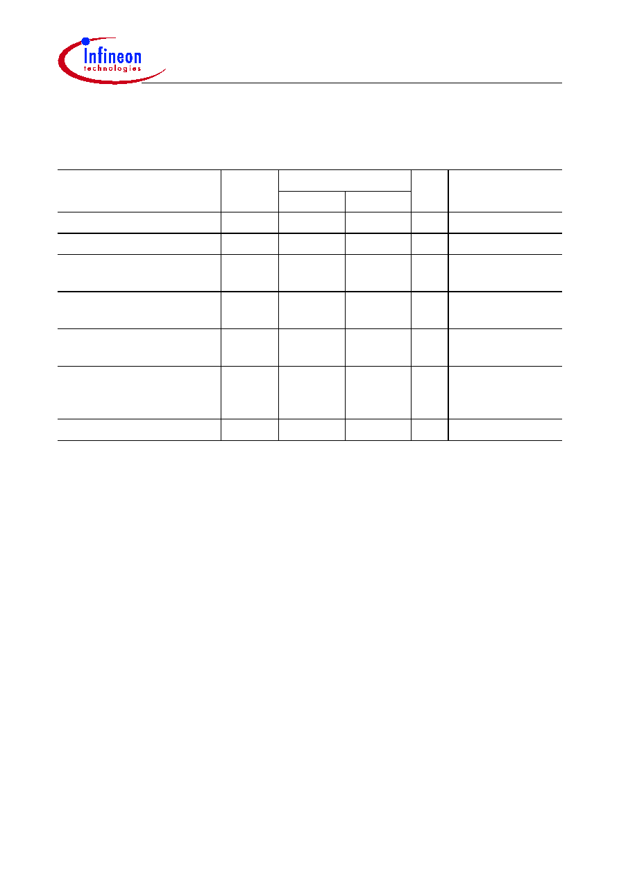
C161CS/JC/JI-32R
C161CS/JC/JI-L
Data Sheet
49
V3.0, 2001-01
Absolute Maximum Ratings
Note: Stresses above those listed under "Absolute Maximum Ratings" may cause
permanent damage to the device. This is a stress rating only and functional
operation of the device at these or any other conditions above those indicated in
the operational sections of this specification is not implied. Exposure to absolute
maximum rating conditions for extended periods may affect device reliability.
During absolute maximum rating overload conditions (
V
IN
>
V
DD
or
V
IN
<
V
SS
) the
voltage on
V
DD
pins with respect to ground (
V
SS
) must not exceed the values
defined by the absolute maximum ratings.
Table 8
Absolute Maximum Rating Parameters
Parameter
Symbol
Limit Values
Unit Notes
min.
max.
Storage temperature
T
ST
-65
150
�
C
�
Junction temperature
T
J
-40
150
�
C
under bias
Voltage on
V
DD
pins with
respect to ground (
V
SS
)
V
DD
-0.5
6.5
V
�
Voltage on any pin with
respect to ground (
V
SS
)
V
IN
-0.5
V
DD
+ 0.5 V
�
Input current on any pin
during overload condition
�
-10
10
mA
�
Absolute sum of all input
currents during overload
condition
�
�
|100|
mA
�
Power dissipation
P
DISS
�
1.5
W
�
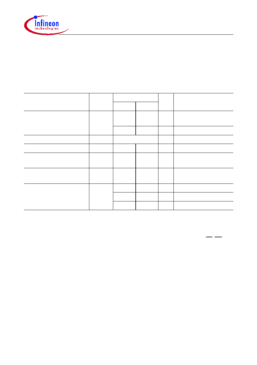
C161CS/JC/JI-32R
C161CS/JC/JI-L
Data Sheet
50
V3.0, 2001-01
Operating Conditions
The following operating conditions must not be exceeded in order to ensure correct
operation of the C161CS/JC/JI. All parameters specified in the following sections refer
to these operating conditions, unless otherwise noticed.
Table 9
Operating Condition Parameters
Parameter
Symbol
Limit Values
Unit Notes
min.
max.
Digital supply voltage
V
DD
4.5
5.5
V
Active mode,
f
CPUmax
= 25 MHz
2.5
1)
1)
Output voltages and output currents will be reduced when
V
DD
leaves the range defined for active mode.
5.5
V
PowerDown mode
Digital ground voltage
V
SS
0
V
Reference voltage
Overload current
I
OV
�
�
5
mA
Per pin
2)3)4)
2)
Overload conditions occur if the standard operatings conditions are exceeded, i.e. the voltage on any pin
exceeds the specified range (i.e.
V
OV
>
V
DD
+ 0.5 V or
V
OV
<
V
SS
- 0.5 V). The absolute sum of input overload
currents on all pins may not exceed 50 mA. The supply voltage must remain within the specified limits.
Proper operation is not guaranteed if overload conditions occur on functional pins line XTAL1, RD, WR, etc.
3)
Not 100% tested, guaranteed by design and characterization.
4)
Due to the different port structure of Port 9 (required by the IIC bus specification) the pins of Port 9 can only
tolerate positive overload current, i.e.
V
OV
>
V
SS
- 0.5 V.
Absolute sum of overload
currents
|
I
OV
|
�
50
mA
3)
External Load
Capacitance
C
L
�
100
pF
Pin drivers in
fast edge mode
5)
5)
The timing is valid for pin drivers in high current or dynamic current mode. The reduced static output current
in dynamic current mode must be respected when designing the system.
Ambient temperature
T
A
0
70
�
C
SAB-C161CS/JC/JI ...
-40
85
�
C
SAF-C161CS/JC/JI ...
-40
125
�
C
SAK-C161CS/JC/JI ...
C161CS/JC/JI-32R
C161CS/JC/JI-L
Data Sheet
51
V3.0, 2001-01
Parameter Interpretation
The parameters listed in the following partly represent the characteristics of the C161CS/
JC/JI and partly its demands on the system. To aid in interpreting the parameters right,
when evaluating them for a design, they are marked in column "Symbol":
CC (Controller Characteristics):
The logic of the C161CS/JC/JI will provide signals with the respective timing
characteristics.
SR (System Requirement):
The external system must provide signals with the respective timing characteristics to
the C161CS/JC/JI.
DC Characteristics
(Operating Conditions apply)
1)
Parameter
Symbol
Limit Values
Unit Test Condition
min.
max.
Input low voltage (TTL,
all except XTAL1, XTAL3, Port 9)
V
IL
SR -0.5
0.2
V
DD
- 0.1
V
�
Input low voltage
XTAL1, XTAL3, Port 9
V
IL2
SR -0.5
0.3
V
DD
V
�
Input low voltage
(Special Threshold)
V
ILS
SR -0.5
2.0
V
�
Input high voltage (TTL, all
except RSTIN, XTAL1, XTAL3,
Port 9)
V
IH
SR 0.2
V
DD
+ 0.9
V
DD
+
0.5
V
�
Input high voltage RSTIN
(when operated as input)
V
IH1
SR 0.6
V
DD
V
DD
+
0.5
V
�
Input high voltage
XTAL1, XTAL3, Port 9
V
IH2
SR 0.7
V
DD
V
DD
+
0.5
V
�
Input high voltage
(Special Threshold)
V
IHS
SR 0.8
V
DD
- 0.2
V
DD
+
0.5
V
�
Input Hysteresis
(Special Threshold)
HYS
400
�
mV
Series resistance
= 0
Output low voltage
(PORT0, PORT1, Port 4, ALE,
RD, WR, BHE, CLKOUT,
RSTOUT, RSTIN
2)
)
V
OL
CC �
0.45
V
I
OL
= 2.4 mA
3)
I
OL
= 0.5 mA
4)
Output low voltage
(Port 9)
V
OL9
CC �
0.4
V
I
OL
= 3.0 mA
C161CS/JC/JI-32R
C161CS/JC/JI-L
Data Sheet
52
V3.0, 2001-01
Output low voltage
(all other outputs)
V
OL1
CC �
0.45
V
I
OL
= 1.6 mA
3)
I
OL
= 1.6 mA
4)
Output high voltage
5)
(PORT0, PORT1, Port 4, ALE,
RD, WR, BHE, CLKOUT,
RSTOUT)
V
OH
CC 2.4
�
V
I
OH
= -2.4 mA
3)
I
OH
= -0.5 mA
4)
0.9
V
DD
�
V
I
OH
= -0.5 mA
3)
Output high voltage
5)
(all other outputs)
V
OH1
CC 2.4
�
V
I
OH
= -1.6 mA
3)
I
OH
= -0.5 mA
4)
0.9
V
DD
�
V
I
OH
= -0.5 mA
3)
Input leakage current (Port 5)
I
OZ1
CC �
�
200
nA
0 V <
V
IN
<
V
DD
Input leakage current (all other)
I
OZ2
CC �
�
500
nA
0.45 V <
V
IN
<
V
DD
RSTIN inactive current
6)
I
RSTH
7)
�
-10
�
A
V
IN
=
V
IH1
RSTIN active current
6)
I
RSTL
8)
-100
�
�
A
V
IN
=
V
IL
READY/RD/WR inact. current
9)
I
RWH
7)
�
-40
�
A
V
OUT
= 2.4 V
READY/RD/WR active current
9)
I
RWL
8)
-500
�
�
A
V
OUT
=
V
OLmax
ALE inactive current
9)
I
ALEL
7)
�
40
�
A
V
OUT
=
V
OLmax
ALE active current
9)
I
ALEH
8)
500
�
�
A
V
OUT
= 2.4 V
Port 6 inactive current
9)
I
P6H
7)
�
-40
�
A
V
OUT
= 2.4 V
Port 6 active current
9)
I
P6L
8)
-500
�
�
A
V
OUT
=
V
OL1max
PORT0 configuration current
10)
I
P0H
7)
�
-10
�
A
V
IN
=
V
IHmin
I
P0L
8)
-100
�
�
A
V
IN
=
V
ILmax
XTAL1 input current
I
IL
CC �
�
20
�
A
0 V <
V
IN
<
V
DD
Pin capacitance
11)
(digital inputs/outputs)
C
IO
CC �
10
pF
f
= 1 MHz
T
A
= 25
�
C
1)
Keeping signal levels within the levels specified in this table, ensures operation without overload conditions.
For signal levels outside these specifications also refer to the specification of the overload current
I
OV
.
2)
Valid in bidirectional reset mode only.
3)
This output current may be drawn from (output) pins operating in High Current mode.
4)
This output current may be drawn from (output) pins operating in Low Current mode.
5)
This specification is not valid for outputs which are switched to open drain mode. In this case the respective
output will float and the voltage results from the external circuitry.
DC Characteristics (cont'd)
(Operating Conditions apply)
1)
Parameter
Symbol
Limit Values
Unit Test Condition
min.
max.

C161CS/JC/JI-32R
C161CS/JC/JI-L
Data Sheet
53
V3.0, 2001-01
6)
These parameters describe the RSTIN pullup, which equals a resistance of ca. 50 to 250 k
.
7)
The maximum current may be drawn while the respective signal line remains inactive.
8)
The minimum current must be drawn in order to drive the respective signal line active.
9)
This specification is valid during Reset and during Hold-mode or Adapt-mode. During Hold-mode Port 6 pins
are only affected, if they are used (configured) for CS output and the open drain function is not enabled. The
READY-pullup is always active, except for Powerdown mode.
10)
This specification is valid during Reset and during Adapt-mode.
11)
Not 100% tested, guaranteed by design and characterization.
Power Consumption C161CS/JC/JI
(Operating Conditions apply)
Parameter
Symbol
Limit Values
Unit Test Condition
min.
max.
Power supply current (active)
with all peripherals active
I
DD
�
15 +
2.5
�
f
CPU
mA
RSTIN =
V
IL
f
CPU
in [MHz]
1)
1)
The supply current is a function of the operating frequency. This dependency is illustrated in
Figure 10
.
These parameters are tested at
V
DDmax
and maximum CPU clock with all outputs disconnected and all inputs
at
V
IL
or
V
IH
.
Idle mode supply current
with all peripherals active
I
IDX
�
5 +
1.5
�
f
CPU
mA
RSTIN =
V
IH1
f
CPU
in [MHz]
1)
Idle mode supply curr., Main osc,
with all peripherals deactivated,
PLL off, SDD factor = 32
I
IDOM
2)
2)
This parameter is determined mainly by the current consumed by the oscillator (see
Figure 9
). This current,
however, is influenced by the external oscillator circuitry (crystal, capacitors). The values given refer to a typical
circuitry and may change in case of a not optimized external oscillator circuitry.
�
500 +
50
�
f
OSC
�
A
RSTIN =
V
IH1
f
OSC
in [MHz]
1)
Idle mode supply curr., Aux. osc,
with all peripherals deactivated,
PLL off, SDD factor = 32
I
IDOA
2)
�
100
�
A
V
DD
=
V
DDmax
f
OSC
= 32 kHz
3)
3)
This parameter is tested including leakage currents. All inputs (including pins configured as inputs) at 0 V to
0.1 V or at
V
DD
- 0.1 V to
V
DD
, all outputs (including pins configured as outputs) disconnected.
Sleep and Power-down mode
supply current with RTC running
on main oscillator
I
PDRM
2)
�
200 +
25
�
f
OSC
�
A
V
DD
=
V
DDmax
f
OSC
in [MHz]
3)
Sleep and Power-down mode
supply current with RTC disabled
I
PDO
�
50
�
A
V
DD
=
V
DDmax
3)
C161CS/JC/JI-32R
C161CS/JC/JI-L
Data Sheet
54
V3.0, 2001-01
Figure 9
Idle and Power Down Supply Current as a Function of Oscillator
Frequency
MCD04453
f
OSC
0
�A
0
4
8
12
16
250
500
750
1000
1250
1500
MHz
I
I
IDOMmax
I
IDOMtyp
I
PDRMmax
I
PDOmax
I
IDOAmax
C161CS/JC/JI-32R
C161CS/JC/JI-L
Data Sheet
55
V3.0, 2001-01
Figure 10
Supply/Idle Current as a Function of Operating Frequency
I
[mA]
f
CPU
[MHz]
10
15
20
25
I
DD5max
I
DD5typ
I
IDX5max
I
IDX5typ
20
40
60
80
100
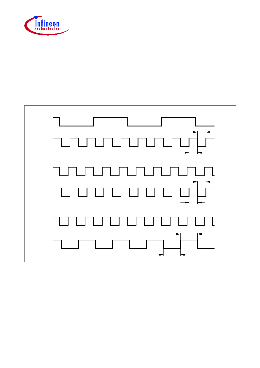
C161CS/JC/JI-32R
C161CS/JC/JI-L
Data Sheet
56
V3.0, 2001-01
AC Characteristics
Definition of Internal Timing
The internal operation of the C161CS/JC/JI is controlled by the internal CPU clock
f
CPU
.
Both edges of the CPU clock can trigger internal (e.g. pipeline) or external (e.g. bus
cycles) operations.
The specification of the external timing (AC Characteristics) therefore depends on the
time between two consecutive edges of the CPU clock, called "TCL" (see
Figure 11
).
Figure 11
Generation Mechanisms for the CPU Clock
The CPU clock signal
f
CPU
can be generated from the oscillator clock signal
f
OSC
via
different mechanisms. The duration of TCLs and their variation (and also the derived
external timing) depends on the used mechanism to generate
f
CPU
. This influence must
be regarded when calculating the timings for the C161CS/JC/JI.
Note: The example for PLL operation shown in the fig. above refers to a PLL factor of 4.
The used mechanism to generate the basic CPU clock is selected by bitfield CLKCFG
in register RP0H.7-5.
Upon a long hardware reset register RP0H is loaded with the logic levels present on the
upper half of PORT0 (P0H), i.e. bitfield CLKCFG represents the logic levels on pins
MCT04338
f
OSC
f
CPU
Phase Locked Loop Operation
TCL
f
OSC
f
CPU
Direct Clock Drive
f
OSC
f
CPU
Prescaler Operation
TCL
TCL
TCL
TCL
TCL

C161CS/JC/JI-32R
C161CS/JC/JI-L
Data Sheet
57
V3.0, 2001-01
P0.15-13 (P0H.7-5). Register RP0H can be loaded from the upper half of register
RSTCON under software control.
Table 10
associates the combinations of these three bits with the respective clock
generation mode.
Prescaler Operation
When prescaler operation is configured (CLKCFG = 001
B
) the CPU clock is derived from
the internal oscillator (input clock signal) by a 2:1 prescaler.
The frequency of
f
CPU
is half the frequency of
f
OSC
and the high and low time of
f
CPU
(i.e. the duration of an individual TCL) is defined by the period of the input clock
f
OSC
.
The timings listed in the AC Characteristics that refer to TCLs therefore can be
calculated using the period of
f
OSC
for any TCL.
Phase Locked Loop
When PLL operation is configured (via CLKCFG) the on-chip phase locked loop is
enabled and provides the CPU clock (see table above). The PLL multiplies the input
frequency by the factor F which is selected via the combination of pins P0.15-13 (i.e.
f
CPU
=
f
OSC
�
F). With every F'th transition of
f
OSC
the PLL circuit synchronizes the CPU
clock to the input clock. This synchronization is done smoothly, i.e. the CPU clock
frequency does not change abruptly.
Due to this adaptation to the input clock the frequency of
f
CPU
is constantly adjusted so
it is locked to
f
OSC
. The slight variation causes a jitter of
f
CPU
which also effects the
duration of individual TCLs.
Table 10
C161CS/JC/JI Clock Generation Modes
CLKCFG
(P0H.7-5)
CPU Frequency
f
CPU
=
f
OSC
�
F
External Clock
Input Range
1)
1)
The external clock input range refers to a CPU clock range of 10 ... 25 MHz.
Notes
1 1 1
f
OSC
�
4
2.5 to 6.25 MHz
Default configuration
1 1 0
f
OSC
�
3
3.33 to 8.33 MHz
�
1 0 1
f
OSC
�
2
5 to 12.5 MHz
�
1 0 0
f
OSC
�
5
2 to 5 MHz
�
0 1 1
f
OSC
�
1
1 to 25 MHz
Direct drive
2)
2)
The maximum frequency depends on the duty cycle of the external clock signal.
0 1 0
f
OSC
�
1.5
6.66 to 16.6 MHz
�
0 0 1
f
OSC
/ 2
2 to 50 MHz
CPU clock via prescaler
0 0 0
f
OSC
�
2.5
4 to 10 MHz
�

C161CS/JC/JI-32R
C161CS/JC/JI-L
Data Sheet
58
V3.0, 2001-01
The timings listed in the AC Characteristics that refer to TCLs therefore must be
calculated using the minimum TCL that is possible under the respective circumstances.
The actual minimum value for TCL depends on the jitter of the PLL. As the PLL is
constantly adjusting its output frequency so it corresponds to the applied input frequency
(crystal or oscillator) the relative deviation for periods of more than one TCL is lower than
for one single TCL (see formula and
Figure 12
).
For a period of
N
�
TCL the minimum value is computed using the corresponding
deviation D
N
:
(
N
�
TCL)
min
=
N
�
TCL
NOM
- D
N
D
N
[ns] =
�
(13.3 +
N
�
6.3) /
f
CPU
[MHz],
where
N
= number of consecutive TCLs
and 1
N
40.
So for a period of 3 TCLs @ 25 MHz (i.e.
N
= 3): D
3
= (13.3 +
3
�
6.3) / 25 = 1.288 ns,
and (3TCL)
min
= 3TCL
NOM
- 1.288 ns = 58.7 ns (@
f
CPU
= 25 MHz).
This is especially important for bus cycles using waitstates and e.g. for the operation of
timers, serial interfaces, etc. For all slower operations and longer periods (e.g. pulse
train generation or measurement, lower baudrates, etc.) the deviation caused by the PLL
jitter is neglectible.
Note: For all periods longer than 40 TCL the N = 40 value can be used (see
Figure 12
).
Figure 12
Approximated Maximum Accumulated PLL Jitter
MCD04455
N
Max. jitter
D
N
�1
�10
�20
�30
ns
�26.5
1
10
20
40
This approximated formula is valid for
1
N
40 and 10 MHz
f
CPU
25 MHz.
10 MHz
16 MHz
20 MHz
25 MHz
30
<
�
<
�
<
�
<
�

C161CS/JC/JI-32R
C161CS/JC/JI-L
Data Sheet
59
V3.0, 2001-01
Direct Drive
When direct drive is configured (CLKCFG = 011
B
) the on-chip phase locked loop is
disabled and the CPU clock is directly driven from the internal oscillator with the input
clock signal.
The frequency of
f
CPU
directly follows the frequency of
f
OSC
so the high and low time of
f
CPU
(i.e. the duration of an individual TCL) is defined by the duty cycle of the input clock
f
OSC
.
The timings listed below that refer to TCLs therefore must be calculated using the
minimum TCL that is possible under the respective circumstances. This minimum value
can be calculated via the following formula:
TCL
min
= 1/
f
OSC
�
DC
min
(DC = duty cycle)
For two consecutive TCLs the deviation caused by the duty cycle of
f
OSC
is
compensated so the duration of 2TCL is always 1/
f
OSC
. The minimum value TCL
min
therefore has to be used only once for timings that require an odd number of TCLs (1, 3,
...). Timings that require an even number of TCLs (2, 4, ...) may use the formula
2TCL = 1/
f
OSC
.
Note: The address float timings in Multiplexed bus mode (
t
11
and
t
45
) use the maximum
duration of TCL (TCL
max
= 1/
f
OSC
�
DC
max
) instead of TCL
min
.
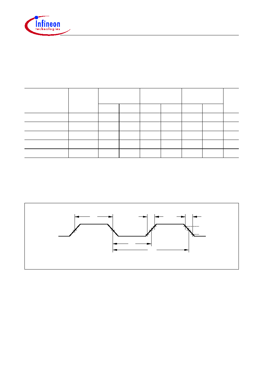
C161CS/JC/JI-32R
C161CS/JC/JI-L
Data Sheet
60
V3.0, 2001-01
AC Characteristics
External Clock Drive XTAL1 (Main Oscillator)
(Operating Conditions apply)
Figure 13
External Clock Drive XTAL1
Note: If the on-chip oscillator is used together with a crystal, the oscillator frequency is
limited to a range of 4 MHz to 16 MHz.
It is strongly recommended to measure the oscillation allowance (or margin) in the
final target system (layout) to determine the optimum parameters for the oscillator
operation. Please refer to the limits specified by the crystal supplier.
When driven by an external clock signal it will accept the specified frequency
range. Operation at lower input frequencies is possible but is guaranteed by
design only (not 100% tested).
Table 11
External Clock Drive Characteristics
Parameter
Symbol
Direct Drive
1:1
Prescaler
2:1
PLL
1:N
Unit
min.
max.
min.
max.
min.
max.
Oscillator period
t
OSCM
SR 40
�
20
�
60
1)
1)
The minimum and maximum oscillator periods for PLL operation depend on the selected CPU clock generation
mode. Please see respective table above.
500
1)
ns
High time
2)
2)
The clock input signal must reach the defined levels
V
IL2
and
V
IH2
.
t
1
SR 20
3)
3)
The minimum high and low time refers to a duty cycle of 50%. The maximum operating frequency (
f
CPU
) in
direct drive mode depends on the duty cycle of the clock input signal.
�
6
�
10
�
ns
Low time
2)
t
2
SR 20
3)
�
6
�
10
�
ns
Rise time
2)
t
3
SR �
10
�
6
�
10
ns
Fall time
2)
t
4
SR �
10
�
6
�
10
ns
MCT02534
3
t
4
t
V
IH2
V
IL
V
DD
0.5
1
t
2
t
OSC
t
C161CS/JC/JI-32R
C161CS/JC/JI-L
Data Sheet
61
V3.0, 2001-01
AC Characteristics
External Clock Drive XTAL3 (Auxiliary Oscillator)
(Operating Conditions apply)
Note: The auxiliary oscillator is optimized for oscillation with a crystal at a frequency of
32 kHz. When driven by an external clock signal it will accept the specified
frequency range.
Operation at lower input frequencies is possible but is guaranteed by design only
(not 100% tested).
Table 12
AC Characteristics
Parameter
Symbol
Optimum Input Clock
= 32 kHz
Variable Input Clock
1 /
t
OSCA
= 10 to 50 kHz
Unit
min.
max.
min.
max.
Oscillator period
t
OSCA
SR 31
31
20
100
�
s
High time
t
1
SR 6
1)
1)
The clock input signal must reach the defined levels
V
IL
and
V
IH2
.
�
0.2
�
t
OSCA
1)
�
�
s
Low time
t
2
SR 6
1)
�
0.2
�
t
OSCA
1)
�
�
s
Rise time
t
3
SR �
12
�
0.4
�
t
OSCA
�
s
Fall time
t
4
SR �
12
�
0.4
�
t
OSCA
�
s
C161CS/JC/JI-32R
C161CS/JC/JI-L
Data Sheet
62
V3.0, 2001-01
A/D Converter Characteristics
(Operating Conditions apply)
Table 13
A/D Converter Characteristics
Parameter
Symbol
Limit Values
Unit Test
Condition
min.
max.
Analog reference supply
V
AREF
SR 4.0
V
DD
+ 0.1 V
1)
1)
TUE is tested at
V
AREF
= 5.0 V,
V
AGND
= 0 V,
V
DD
= 4.9 V. It is guaranteed by design for all other voltages
within the defined voltage range.
If the analog reference supply voltage exceeds the power supply voltage by up to 0.2 V
(i.e.
V
AREF
=
V
DD
= +0.2 V) the maximum TUE is increased to
�
3 LSB. This range is not 100% tested.
The specified TUE is guaranteed only if the absolute sum of input overload currents on Port 5 pins (see
I
OV
specification) does not exceed 10 mA.
During the reset calibration sequence the maximum TUE may be
�
4 LSB.
Analog reference ground
V
AGND
SR
V
SS
- 0.1
V
SS
+ 0.2 V
Analog input voltage range
V
AIN
SR
V
AGND
V
AREF
V
2)
2)
V
AIN
may exceed
V
AGND
or
V
AREF
up to the absolute maximum ratings. However, the conversion result in
these cases will be X000
H
or X3FF
H
, respectively.
Basic clock frequency
f
BC
0.5
6.25
MHz
3)
3)
The limit values for
f
BC
must not be exceeded when selecting the CPU frequency and the ADCTC setting.
Conversion time
t
C
CC �
40
t
BC
+
t
S
+ 2
t
CPU
�
4)
t
CPU
= 1 /
f
CPU
4)
This parameter includes the sample time
t
S
, the time for determining the digital result and the time to load the
result register with the conversion result.
Values for the basic clock
t
BC
depend on programming and can be taken from
Table 14
.
This parameter depends on the ADC control logic. It is not a real maximum value, but rather a fixum.
Calibration time after reset
t
CAL
CC �
3328
t
BC
�
5)
5)
During the reset calibration conversions can be executed (with the current accuracy). The time required for
these conversions is added to the total reset calibration time.
Total unadjusted error
TUE
CC �
�
2
LSB
1)
Internal resistance of
reference voltage source
R
AREF
SR �
t
BC
/ 60
- 0.25
k
t
BC
in [ns]
6)7)
6)
During the conversion the ADC's capacitance must be repeatedly charged or discharged. The internal
resistance of the reference voltage source must allow the capacitance to reach its respective voltage level
within each conversion step. The maximum internal resistance results from the programmed conversion
timing.
7)
Not 100% tested, guaranteed by design and characterization.
Internal resistance of analog
source
R
ASRC
SR �
t
S
/ 450
- 0.25
k
t
S
in [ns]
7)8)
ADC input capacitance
C
AIN
CC �
33
pF
7)
C161CS/JC/JI-32R
C161CS/JC/JI-L
Data Sheet
63
V3.0, 2001-01
Sample time and conversion time of the C161CS/JC/JI's A/D Converter are
programmable.
Table 14
should be used to calculate the above timings.
The limit values for
f
BC
must not be exceeded when selecting ADCTC.
Converter Timing Example:
Assumptions:
f
CPU
= 25 MHz (i.e.
t
CPU
= 40 ns), ADCTC = `00', ADSTC = `00'.
Basic clock
f
BC
=
f
CPU
/ 4 = 6.25 MHz, i.e.
t
BC
= 160 ns.
Sample time
t
S
=
t
BC
�
8 = 1280 ns.
Conversion time
t
C
=
t
S
+ 40
t
BC
+ 2
t
CPU
= (1280 + 6400 + 80) ns = 7.8
�
s.
8)
During the sample time the input capacitance
C
AIN
can be charged/discharged by the external source. The
internal resistance of the analog source must allow the capacitance to reach its final voltage level within
t
S
.
After the end of the sample time
t
S
, changes of the analog input voltage have no effect on the conversion
result.
Values for the sample time
t
S
depend on programming and can be taken from
Table 14
.
Table 14
A/D Converter Computation Table
ADCON.15|14
(ADCTC)
A/D Converter
Basic Clock
f
BC
ADCON.13|12
(ADSTC)
Sample time
t
S
00
f
CPU
/ 4
00
t
BC
�
8
01
f
CPU
/ 2
01
t
BC
�
16
10
f
CPU
/ 16
10
t
BC
�
32
11
f
CPU
/ 8
11
t
BC
�
64
C161CS/JC/JI-32R
C161CS/JC/JI-L
Data Sheet
64
V3.0, 2001-01
Testing Waveforms
Figure 14
Input Output Waveforms
Figure 15
Float Waveforms
MCA04414
2.4 V
0.45 V
1.8 V
0.8 V
1.8 V
0.8 V
Test Points
AC inputs during testing are driven at 2.4 V for a logic 1' and 0.45 V for a logic 0'.
Timing measurements are made at
IH
V
min for a logic 1' and
V
IL
max for a logic 0'.
'
'
'
'
MCA00763
- 0.1 V
+ 0.1 V
+ 0.1 V
- 0.1 V
Reference
For timing purposes a port pin is no longer floating when a 100 mV change from load voltage occurs,
but begins to float when a 100 mV change from the loaded
OH
V
Timing
Points
Load
V
V
Load
OH
V
V
OL
/
V
OL
level occurs (
I
OH
OL
I
/
= 20 mA).
C161CS/JC/JI-32R
C161CS/JC/JI-L
Data Sheet
65
V3.0, 2001-01
Memory Cycle Variables
The timing tables below use three variables which are derived from the BUSCONx
registers and represent the special characteristics of the programmed memory cycle.
The following table describes, how these variables are to be computed.
Note: Please respect the maximum operating frequency of the respective derivative.
AC Characteristics
Table 15
Memory Cycle Variables
Description
Symbol
Values
ALE Extension
t
A
TCL
�
<ALECTL>
Memory Cycle Time Waitstates
t
C
2TCL
�
(15 - <MCTC>)
Memory Tristate Time
t
F
2TCL
�
(1 - <MTTC>)
Multiplexed Bus
(Operating Conditions apply)
ALE cycle time = 6 TCL + 2
t
A
+
t
C
+
t
F
(120 ns at 25 MHz CPU clock without waitstates)
Parameter
Symbol
Max. CPU Clock
= 25 MHz
Variable CPU Clock
1 / 2TCL = 1 to 25 MHz
Unit
min.
max.
min.
max.
ALE high time
t
5
CC
10 +
t
A
�
TCL - 10
+
t
A
�
ns
Address setup to ALE
t
6
CC
4 +
t
A
�
TCL - 16
+
t
A
�
ns
Address hold after ALE
t
7
CC
10 +
t
A
�
TCL - 10
+
t
A
�
ns
ALE falling edge to RD,
WR (with RW-delay)
t
8
CC
10 +
t
A
�
TCL - 10
+
t
A
�
ns
ALE falling edge to RD,
WR (no RW-delay)
t
9
CC
-10 +
t
A
�
-10 +
t
A
�
ns
Address float after RD,
WR (with RW-delay)
t
10
CC
�
6
�
6
ns
Address float after RD,
WR (no RW-delay)
t
11
CC
�
26
�
TCL + 6
ns
RD, WR low time
(with RW-delay)
t
12
CC
30 +
t
C
�
2TCL - 10
+
t
C
�
ns
C161CS/JC/JI-32R
C161CS/JC/JI-L
Data Sheet
66
V3.0, 2001-01
RD, WR low time
(no RW-delay)
t
13
CC
50 +
t
C
�
3TCL - 10
+
t
C
�
ns
RD to valid data in
(with RW-delay)
t
14
SR
�
20 +
t
C
�
2TCL - 20
+
t
C
ns
RD to valid data in
(no RW-delay)
t
15
SR
�
40 +
t
C
�
3TCL - 20
+
t
C
ns
ALE low to valid data in
t
16
SR
�
40 +
t
A
+
t
C
�
3TCL - 20
+
t
A
+
t
C
ns
Address to valid data in
t
17
SR
�
50 + 2
t
A
+
t
C
�
4TCL - 30
+
2
t
A
+
t
C
ns
Data hold after RD
rising edge
t
18
SR
0
�
0
�
ns
Data float after RD
t
19
SR
�
26 +
t
F
�
2TCL - 14
+
t
F
ns
Data valid to WR
t
22
CC
20 +
t
C
�
2TCL - 20
+
t
C
�
ns
Data hold after WR
t
23
CC
26 +
t
F
�
2TCL - 14
+
t
F
�
ns
ALE rising edge after RD,
WR
t
25
CC
26 +
t
F
�
2TCL - 14
+
t
F
�
ns
Address hold after RD,
WR
t
27
CC
26 +
t
F
�
2TCL - 14
+
t
F
�
ns
ALE falling edge to CS
1)
t
38
CC
-4 -
t
A
10 -
t
A
-4 -
t
A
10 -
t
A
ns
CS low to Valid Data In
1)
t
39
SR
�
40
+
t
C
+
2
t
A
�
3TCL - 20
+
t
C
+ 2
t
A
ns
CS hold after RD, WR
1)
t
40
CC
46 +
t
F
�
3TCL - 14
+
t
F
�
ns
ALE fall. edge to RdCS,
WrCS (with RW delay)
t
42
CC
16 +
t
A
�
TCL - 4
+
t
A
�
ns
Multiplexed Bus (cont'd)
(Operating Conditions apply)
ALE cycle time = 6 TCL + 2
t
A
+
t
C
+
t
F
(120 ns at 25 MHz CPU clock without waitstates)
Parameter
Symbol
Max. CPU Clock
= 25 MHz
Variable CPU Clock
1 / 2TCL = 1 to 25 MHz
Unit
min.
max.
min.
max.
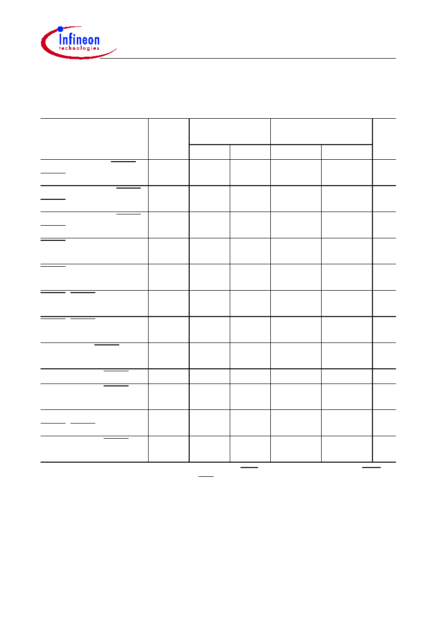
C161CS/JC/JI-32R
C161CS/JC/JI-L
Data Sheet
67
V3.0, 2001-01
ALE fall. edge to RdCS,
WrCS (no RW delay)
t
43
CC
-4 +
t
A
�
-4
+
t
A
�
ns
Address float after RdCS,
WrCS (with RW delay)
t
44
CC
�
0
�
0
ns
Address float after RdCS,
WrCS (no RW delay)
t
45
CC
�
20
�
TCL
ns
RdCS to Valid Data In
(with RW delay)
t
46
SR
�
16 +
t
C
�
2TCL - 24
+
t
C
ns
RdCS to Valid Data In
(no RW delay)
t
47
SR
�
36 +
t
C
�
3TCL - 24
+
t
C
ns
RdCS, WrCS Low Time
(with RW delay)
t
48
CC
30 +
t
C
�
2TCL - 10
+
t
C
�
ns
RdCS, WrCS Low Time
(no RW delay)
t
49
CC
50 +
t
C
�
3TCL - 10
+
t
C
�
ns
Data valid to WrCS
t
50
CC
26 +
t
C
�
2TCL - 14
+
t
C
�
ns
Data hold after RdCS
t
51
SR
0
�
0
�
ns
Data float after RdCS
t
52
SR
�
20 +
t
F
�
2TCL - 20
+
t
F
ns
Address hold after
RdCS, WrCS
t
54
CC
20 +
t
F
�
2TCL - 20
+
t
F
�
ns
Data hold after WrCS
t
56
CC
20 +
t
F
�
2TCL - 20
+
t
F
�
ns
1)
These parameters refer to the latched chip select signals (CSxL). The early chip select signals (CSxE) are
specified together with the address and signal BHE (see figures below).
Multiplexed Bus (cont'd)
(Operating Conditions apply)
ALE cycle time = 6 TCL + 2
t
A
+
t
C
+
t
F
(120 ns at 25 MHz CPU clock without waitstates)
Parameter
Symbol
Max. CPU Clock
= 25 MHz
Variable CPU Clock
1 / 2TCL = 1 to 25 MHz
Unit
min.
max.
min.
max.
C161CS/JC/JI-32R
C161CS/JC/JI-L
Data Sheet
68
V3.0, 2001-01
Figure 16
External Memory Cycle:
Multiplexed Bus, With Read/Write Delay, Normal ALE
Address
Data OUT
Address
Data IN
Address
MCT04439
A23-A16
(A15-A8)
BHE, CSxE
ALE
CSxL
`
BUS
RD
RdCSx
Read Cycle
BUS
Write Cycle
t
5
t
16
t
25
t
38
t
39
t
40
t
27
t
17
t
6
t
7
t
19
t
54
t
18
t
8
t
10
t
12
t
42
t
44
t
52
t
51
t
48
t
23
t
8
t
10
t
14
t
46
t
22
t
56
WR, WRL,
WRH
WrCSx
t
12
t
42
t
44
t
48
t
50
C161CS/JC/JI-32R
C161CS/JC/JI-L
Data Sheet
69
V3.0, 2001-01
Figure 17
External Memory Cycle:
Multiplexed Bus, With Read/Write Delay, Extended ALE
Address
Address
Data OUT
Address
Data IN
MCT04440
A23-A16
(A15-A8)
BHE, CSxE
ALE
CSxL
BUS
RD
RdCSx
Read Cycle
BUS
Write Cycle
t
5
t
16
t
25
t
38
t
39
t
40
t
27
t
17
t
7
t
19
t
54
t
18
t
8
t
10
t
12
t
42
t
44
t
52
t
51
t
48
t
23
t
8
t
10
t
14
t
46
t
22
t
56
WR, WRL,
WRH
WrCSx
t
12
t
42
t
44
t
48
t
50
t
6
C161CS/JC/JI-32R
C161CS/JC/JI-L
Data Sheet
70
V3.0, 2001-01
Figure 18
External Memory Cycle:
Multiplexed Bus, No Read/Write Delay, Normal ALE
Data OUT
Address
Address
Data IN
Address
MCT04441
A23-A16
(A15-A8)
BHE, CSxE
ALE
CSxL
BUS
RD
RdCSx
Read Cycle
BUS
Write Cycle
t
5
t
16
t
25
t
38
t
39
t
40
t
27
t
17
t
6
t
7
t
19
t
54
t
18
t
9
t
11
t
43
t
45
t
52
t
51
t
23
t
22
t
56
WR, WRL,
WRH
WrCSx
t
13
t
49
t
50
t
9
t
11
t
43
t
45
t
15
t
13
t
47
t
49
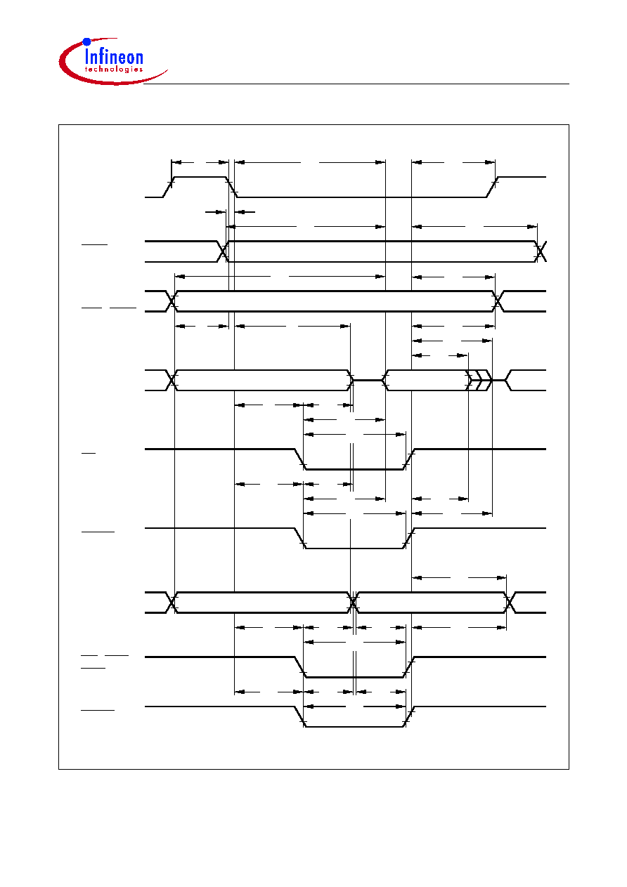
C161CS/JC/JI-32R
C161CS/JC/JI-L
Data Sheet
71
V3.0, 2001-01
Figure 19
External Memory Cycle:
Multiplexed Bus, No Read/Write Delay, Extended ALE
Address
Address
Data OUT
Address
Data IN
MCT04442
A23-A16
(A15-A8)
BHE, CSxE
ALE
CSxL
BUS
RD
RdCSx
Read Cycle
BUS
Write Cycle
t
5
t
16
t
25
t
38
t
39
t
40
t
27
t
17
t
7
t
19
t
54
t
18
t
9
t
11
t
43
t
52
t
51
t
49
t
23
t
9
t
15
t
47
t
22
t
56
WR, WRL,
WRH
WrCSx
t
43
t
49
t
50
t
6
t
13
t
45
t
13
t
11
t
45
C161CS/JC/JI-32R
C161CS/JC/JI-L
Data Sheet
72
V3.0, 2001-01
AC Characteristics
Demultiplexed Bus
(Operating Conditions apply)
ALE cycle time = 4 TCL + 2
t
A
+
t
C
+
t
F
(80 ns at 25 MHz CPU clock without waitstates)
Parameter
Symbol
Max. CPU Clock
= 25 MHz
Variable CPU Clock
1 / 2TCL = 1 to 25 MHz
Unit
min.
max.
min.
max.
ALE high time
t
5
CC
10 +
t
A
�
TCL - 10
+
t
A
�
ns
Address setup to ALE
t
6
CC
4 +
t
A
�
TCL - 16
+
t
A
�
ns
ALE falling edge to RD,
WR (with RW-delay)
t
8
CC
10 +
t
A
�
TCL - 10
+
t
A
�
ns
ALE falling edge to RD,
WR (no RW-delay)
t
9
CC
-10 +
t
A
�
-10
+
t
A
�
ns
RD, WR low time
(with RW-delay)
t
12
CC
30 +
t
C
�
2TCL - 10
+
t
C
�
ns
RD, WR low time
(no RW-delay)
t
13
CC
50 +
t
C
�
3TCL - 10
+
t
C
�
ns
RD to valid data in
(with RW-delay)
t
14
SR
�
20 +
t
C
�
2TCL - 20
+
t
C
ns
RD to valid data in
(no RW-delay)
t
15
SR
�
40 +
t
C
�
3TCL - 20
+
t
C
ns
ALE low to valid data in
t
16
SR
�
40 +
t
A
+
t
C
�
3TCL - 20
+
t
A
+
t
C
ns
Address to valid data in
t
17
SR
�
50 +
2
t
A
+
t
C
�
4TCL - 30
+
2
t
A
+
t
C
ns
Data hold after RD
rising edge
t
18
SR
0
�
0
�
ns
Data float after RD rising
edge (with RW-delay
1)
)
t
20
SR
�
26 +
2
t
A
+
t
F
1)
�
2TCL - 14
+
22
t
A
+
t
F
1)
ns
Data float after RD rising
edge (no RW-delay
1)
)
t
21
SR
�
10 +
2
t
A
+
t
F
1)
�
TCL - 10
+
22
t
A
+
t
F
1)
ns
C161CS/JC/JI-32R
C161CS/JC/JI-L
Data Sheet
73
V3.0, 2001-01
Data valid to WR
t
22
CC
20 +
t
C
�
2TCL - 20
+
t
C
�
ns
Data hold after WR
t
24
CC
10 +
t
F
�
TCL - 10
+
t
F
�
ns
ALE rising edge after RD,
WR
t
26
CC
-10 +
t
F
�
-10 +
t
F
�
ns
Address hold after WR
2)
t
28
CC
0 +
t
F
�
0 +
t
F
�
ns
ALE falling edge to CS
3)
t
38
CC
-4 -
t
A
10 -
t
A
-4 -
t
A
10 -
t
A
ns
CS low to Valid Data In
3)
t
39
SR
�
40 +
t
C
+
2
t
A
�
3TCL - 20
+
t
C
+ 2
t
A
ns
CS hold after RD, WR
3)
t
41
CC
6 +
t
F
�
TCL - 14
+
t
F
�
ns
ALE falling edge to RdCS,
WrCS (with RW-delay)
t
42
CC
16 +
t
A
�
TCL - 4
+
t
A
�
ns
ALE falling edge to RdCS,
WrCS (no RW-delay)
t
43
CC
-4 +
t
A
�
-4
+
t
A
�
ns
RdCS to Valid Data In
(with RW-delay)
t
46
SR
�
16 +
t
C
�
2TCL - 24
+
t
C
ns
RdCS to Valid Data In
(no RW-delay)
t
47
SR
�
36 +
t
C
�
3TCL
- 24
+
t
C
ns
RdCS, WrCS Low Time
(with RW-delay)
t
48
CC
30 +
t
C
�
2TCL - 10
+
t
C
�
ns
RdCS, WrCS Low Time
(no RW-delay)
t
49
CC
50 +
t
C
�
3TCL - 10
+
t
C
�
ns
Data valid to WrCS
t
50
CC
26 +
t
C
�
2TCL - 14
+
t
C
�
ns
Data hold after RdCS
t
51
SR
0
�
0
�
ns
Data float after RdCS
(with RW-delay)
1)
t
53
SR
�
20 +
t
F
�
2TCL - 20
+
2
t
A
+
t
F
1)
ns
Demultiplexed Bus (cont'd)
(Operating Conditions apply)
ALE cycle time = 4 TCL + 2
t
A
+
t
C
+
t
F
(80 ns at 25 MHz CPU clock without waitstates)
Parameter
Symbol
Max. CPU Clock
= 25 MHz
Variable CPU Clock
1 / 2TCL = 1 to 25 MHz
Unit
min.
max.
min.
max.
C161CS/JC/JI-32R
C161CS/JC/JI-L
Data Sheet
74
V3.0, 2001-01
Data float after RdCS
(no RW-delay)
1)
t
68
SR
�
0 +
t
F
�
TCL - 20
+
2
t
A
+
t
F
1)
ns
Address hold after
RdCS, WrCS
t
55
CC
-6 +
t
F
�
-6 +
t
F
�
ns
Data hold after WrCS
t
57
CC
6 +
t
F
�
TCL - 14 +
t
F
�
ns
1)
RW-delay and
t
A
refer to the next following bus cycle (including an access to an on-chip X-Peripheral).
2)
Read data are latched with the same clock edge that triggers the address change and the rising RD edge.
Therefore address changes before the end of RD have no impact on read cycles.
3)
These parameters refer to the latched chip select signals (CSxL). The early chip select signals (CSxE) are
specified together with the address and signal BHE (see figures below).
Demultiplexed Bus (cont'd)
(Operating Conditions apply)
ALE cycle time = 4 TCL + 2
t
A
+
t
C
+
t
F
(80 ns at 25 MHz CPU clock without waitstates)
Parameter
Symbol
Max. CPU Clock
= 25 MHz
Variable CPU Clock
1 / 2TCL = 1 to 25 MHz
Unit
min.
max.
min.
max.
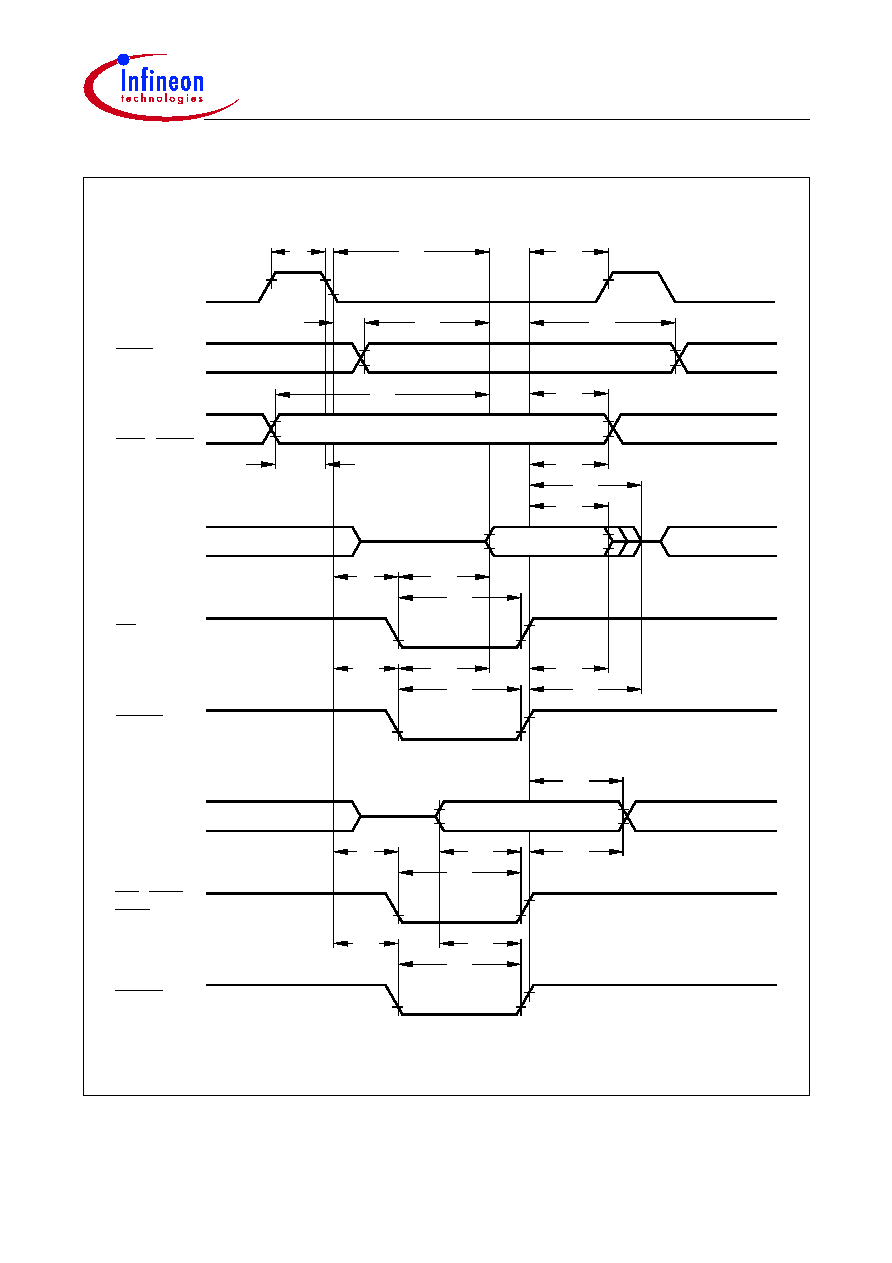
C161CS/JC/JI-32R
C161CS/JC/JI-L
Data Sheet
75
V3.0, 2001-01
Figure 20
External Memory Cycle:
Demultiplexed Bus, With Read/Write Delay, Normal ALE
Data OUT
Address
Data IN
MCT04443
A23-A16
A15-A0
BHE, CSxE
ALE
CSxL
RD
RdCSx
Read Cycle
Write Cycle
t
5
t
16
t
26
t
38
t
39
t
41
t
28
t
17
t
6
t
20
t
55
t
18
t
8
t
12
t
42
t
53
t
51
t
48
t
24
t
8
t
14
t
46
t
22
t
57
WR, WRL,
WRH
WrCSx
t
12
t
42
t
48
t
50
BUS
(D15-D8)
D7-D0
BUS
(D15-D8)
D7-D0
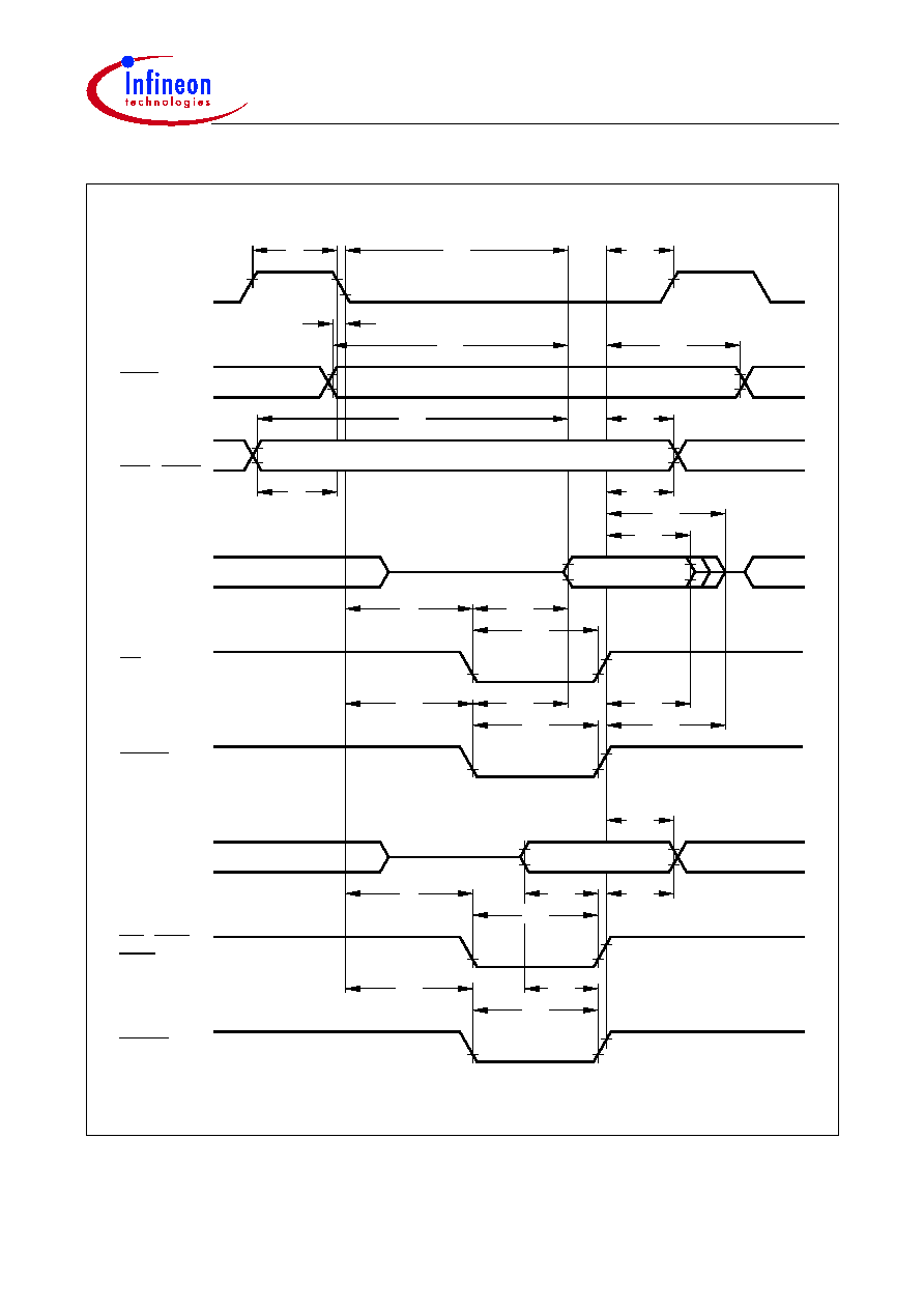
C161CS/JC/JI-32R
C161CS/JC/JI-L
Data Sheet
76
V3.0, 2001-01
Figure 21
External Memory Cycle:
Demultiplexed Bus, With Read/Write Delay, Extended ALE
Address
Data OUT
Data IN
MCT04444
A23-A16
A15-A0
BHE, CSxE
ALE
CSxL
RD
RdCSx
Read Cycle
Write Cycle
t
5
t
16
t
26
t
38
t
39
t
41
t
28
t
17
t
20
t
55
t
18
t
8
t
12
t
42
t
53
t
51
t
48
t
24
t
8
t
14
t
46
t
22
t
57
WR, WRL,
WRH
WrCSx
t
12
t
42
t
48
t
50
t
6
BUS
(D15-D8)
D7-D0
BUS
(D15-D8)
D7-D0
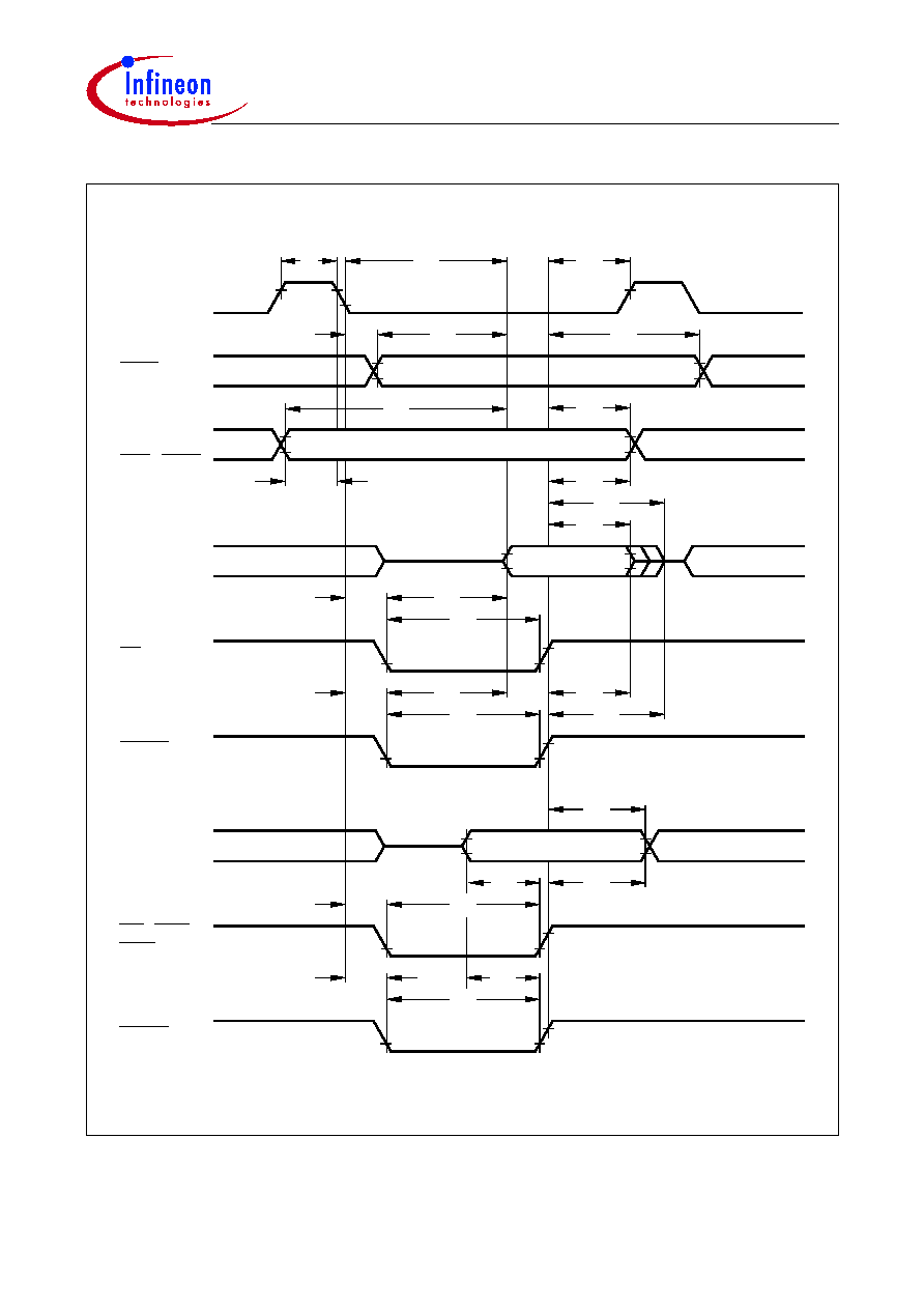
C161CS/JC/JI-32R
C161CS/JC/JI-L
Data Sheet
77
V3.0, 2001-01
Figure 22
External Memory Cycle:
Demultiplexed Bus, No Read/Write Delay, Normal ALE
Data OUT
Address
Data IN
MCT04445
A23-A16
A15-A0
BHE, CSxE
ALE
CSxL
RD
RdCSx
Read Cycle
Write Cycle
t
5
t
16
t
26
t
38
t
39
t
41
t
28
t
17
t
6
t
21
t
55
t
18
t
9
t
13
t
43
t
68
t
51
t
49
t
24
t
15
t
47
t
22
t
57
WR, WRL,
WRH
WrCSx
t
13
t
43
t
49
t
50
BUS
(D15-D8)
D7-D0
BUS
(D15-D8)
D7-D0
t
9
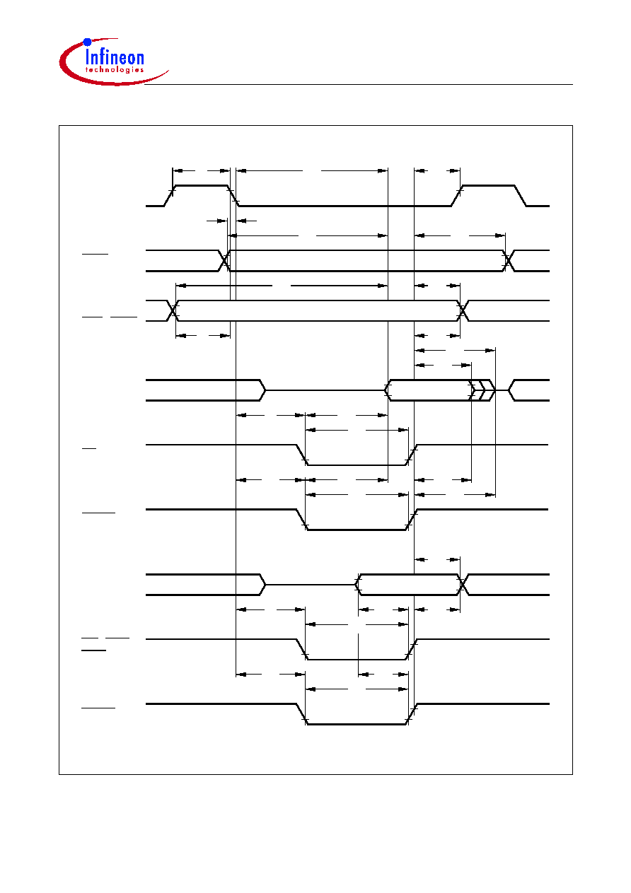
C161CS/JC/JI-32R
C161CS/JC/JI-L
Data Sheet
78
V3.0, 2001-01
Figure 23
External Memory Cycle:
Demultiplexed Bus, No Read/Write Delay, Extended ALE
Address
Data OUT
Data IN
MCT04446
A23-A16
A15-A0
BHE, CSxE
ALE
CSxL
RD
RdCSx
Read Cycle
Write Cycle
t
5
t
16
t
26
t
38
t
39
t
41
t
28
t
17
t
21
t
55
t
18
t
9
t
13
t
43
t
68
t
51
t
49
t
24
t
9
t
15
t
47
t
22
t
57
WR, WRL,
WRH
WrCSx
t
13
t
43
t
49
t
50
t
6
BUS
(D15-D8)
D7-D0
BUS
(D15-D8)
D7-D0

C161CS/JC/JI-32R
C161CS/JC/JI-L
Data Sheet
79
V3.0, 2001-01
AC Characteristics
CLKOUT and READY
(Operating Conditions apply)
Parameter
Symbol
Max. CPU Clock
= 25 MHz
Variable CPU Clock
1 / 2TCL = 1 to 25 MHz
Unit
min.
max.
min.
max.
CLKOUT cycle time
t
29
CC
40
40
2TCL
2TCL
ns
CLKOUT high time
t
30
CC
14
�
TCL - 6
�
ns
CLKOUT low time
t
31
CC
10
�
TCL - 10
�
ns
CLKOUT rise time
t
32
CC
�
4
�
4
ns
CLKOUT fall time
t
33
CC
�
4
�
4
ns
CLKOUT rising edge to
ALE falling edge
t
34
CC
0 +
t
A
10 +
t
A
0 +
t
A
10 +
t
A
ns
Synchronous READY
setup time to CLKOUT
t
35
SR
14
�
14
�
ns
Synchronous READY
hold time after CLKOUT
t
36
SR
4
�
4
�
ns
Asynchronous READY
low time
t
37
SR
54
�
2TCL +
t
58
�
ns
Asynchronous READY
setup time
1)
1)
These timings are given for test purposes only, in order to assure recognition at a specific clock edge.
t
58
SR
14
�
14
�
ns
Asynchronous READY
hold time
1)
t
59
SR
4
�
4
�
ns
Async. READY hold time
after RD, WR high
(Demultiplexed Bus)
2)
2)
Demultiplexed bus is the worst case. For multiplexed bus 2TCL are to be added to the maximum values. This
adds even more time for deactivating READY.
The 2
t
A
and
t
C
refer to the next following bus cycle,
t
F
refers to the current bus cycle.
The maximum limit for
t
60
must be fulfilled if the next following bus cycle is READY controlled.
t
60
SR
0
0
+ 2
t
A
+
t
C
+
t
F
2)
0
TCL - 20
+ 2
t
A
+
t
C
+
t
F
2)
ns
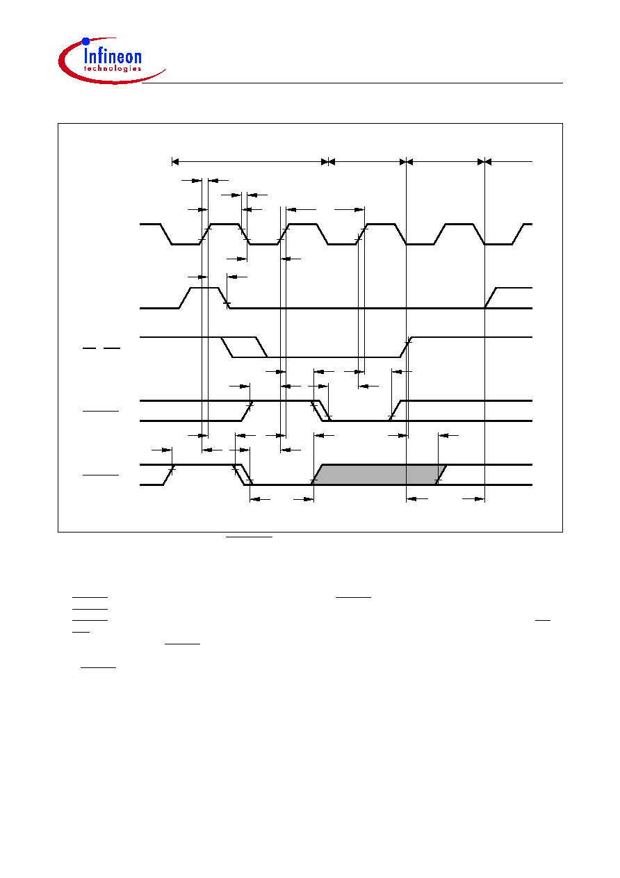
C161CS/JC/JI-32R
C161CS/JC/JI-L
Data Sheet
80
V3.0, 2001-01
Figure 24
CLKOUT and READY
Notes
1)
Cycle as programmed, including MCTC waitstates (Example shows 0 MCTC WS).
2)
The leading edge of the respective command depends on RW-delay.
3)
READY sampled HIGH at this sampling point generates a READY controlled waitstate,
READY sampled LOW at this sampling point terminates the currently running bus cycle.
4)
READY may be deactivated in response to the trailing (rising) edge of the corresponding command (RD or
WR).
5)
If the Asynchronous READY signal does not fulfill the indicated setup and hold times with respect to CLKOUT
(e.g. because CLKOUT is not enabled), it must fulfill
t
37
in order to be safely synchronized. This is guaranteed,
if READY is removed in reponse to the command (see Note
4)
).
6)
Multiplexed bus modes have a MUX waitstate added after a bus cycle, and an additional MTTC waitstate may
be inserted here.
For a multiplexed bus with MTTC waitstate this delay is 2 CLKOUT cycles, for a demultiplexed bus without
MTTC waitstate this delay is zero.
7)
The next external bus cycle may start here.
MCT04447
t
32
CLKOUT
ALE
Command
RD, WR
Sync
READY
Async
READY
t
33
t
29
t
30
t
31
t
34
7)
2)
3)
3)
t
35
t
36
t
35
t
36
t
58
t
59
3)
t
58
t
59
3)
t
37
5)
t
60
4)
see
6)
Running Cycle
1)
READY
Waitstate
MUX/Tristate
6)
C161CS/JC/JI-32R
C161CS/JC/JI-L
Data Sheet
81
V3.0, 2001-01
AC Characteristics
External Bus Arbitration
(Operating Conditions apply)
Parameter
Symbol
Max. CPU Clock
= 25 MHz
Variable CPU Clock
1 / 2TCL = 1 to 25 MHz
Unit
min.
max.
min.
max.
HOLD input setup time
to CLKOUT
t
61
SR
20
�
20
�
ns
CLKOUT to HLDA high
or BREQ low delay
t
62
CC
�
20
�
20
ns
CLKOUT to HLDA low
or BREQ high delay
t
63
CC
�
20
�
20
ns
CSx release
t
64
CC
�
20
�
20
ns
CSx drive
t
65
CC
-4
24
-4
24
ns
Other signals release
t
66
CC
�
20
�
20
ns
Other signals drive
t
67
CC
� 4
24
� 4
24
ns

C161CS/JC/JI-32R
C161CS/JC/JI-L
Data Sheet
82
V3.0, 2001-01
Figure 25
External Bus Arbitration, Releasing the Bus
Notes
1)
The C161CS/JC/JI will complete the currently running bus cycle before granting bus access.
2)
This is the first possibility for BREQ to get active.
3)
The CS outputs will be resistive high (pullup) after
t
64
.
MCT04448
t
61
t
62
CLKOUT
HOLD
HLDA
BREQ
CSx
(On P6.x)
Other
Signals
t
63
t
64
t
66
see
1)
3)
1)
2)
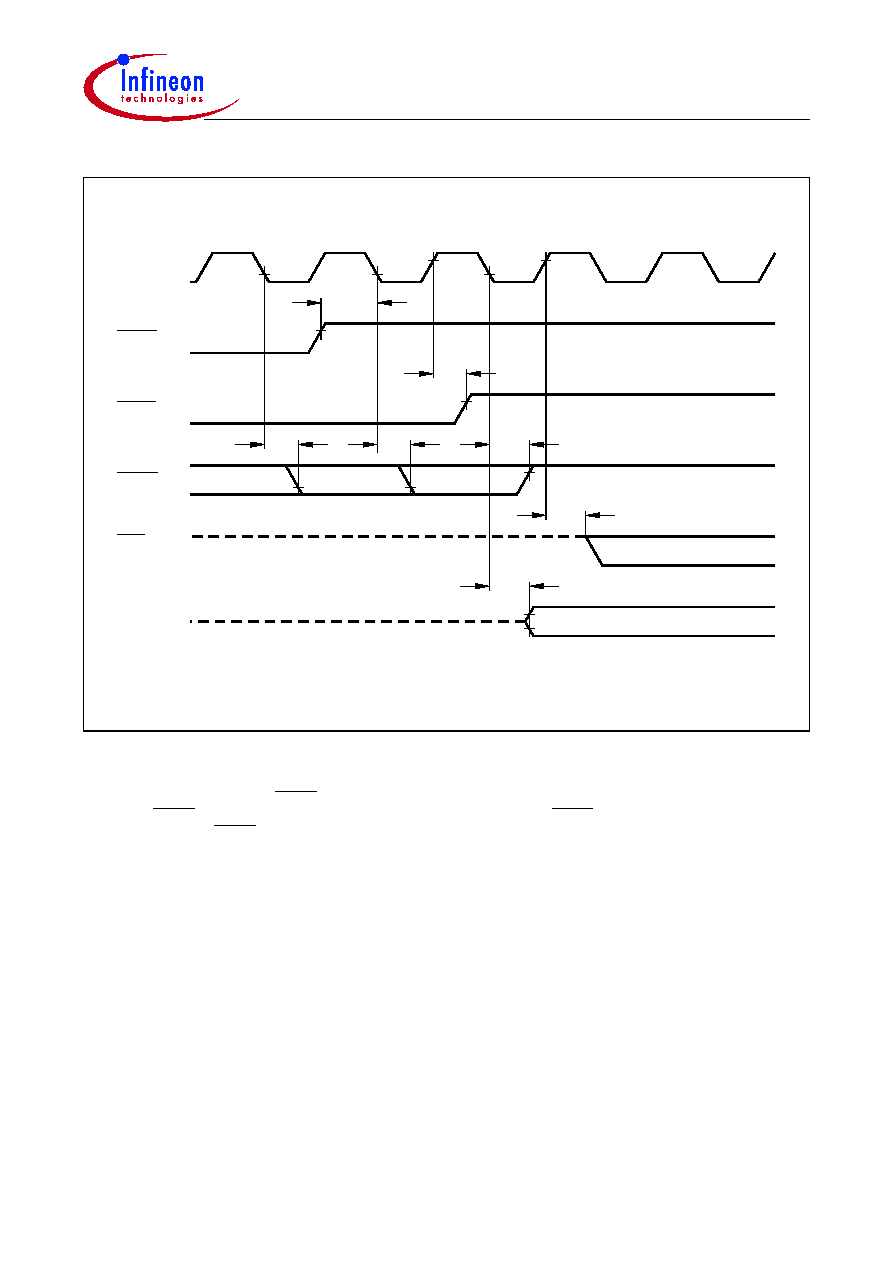
C161CS/JC/JI-32R
C161CS/JC/JI-L
Data Sheet
83
V3.0, 2001-01
Figure 26
External Bus Arbitration, (Regaining the Bus)
Notes
1)
This is the last chance for BREQ to trigger the indicated regain-sequence.
Even if BREQ is activated earlier, the regain-sequence is initiated by HOLD going high.
Please note that HOLD may also be deactivated without the C161CS/JC/JI requesting the bus.
2)
The next C161CS/JC/JI driven bus cycle may start here.
MCT04449
t
61
t
62
t
62
t
62
t
63
t
65
t
67
CLKOUT
HOLD
HLDA
BREQ
CSx
(On P6.x)
Other
Signals
2)
1)

C161CS/JC/JI-32R
C161CS/JC/JI-L
Data Sheet
84
V3.0, 2001-01
Package Outline
P-TQFP-128-2
(Plastic Thin Metric Quad Flat Package)
GPP
09
028
Sorts of Packing
Package outlines for tubes, trays etc. are contained in our
Data Book "Package Information".
Dimensions in mm
SMD = Surface Mounted Device

h t t p : / / w w w . i n f i n e o n . c o m
Published by Infineon Technologies AG
Infineon goes for Business Excellence
"Business excellence means intelligent approaches and clearly
defined processes, which are both constantly under review and
ultimately lead to good operating results.
Better operating results and business excellence mean less
idleness and wastefulness for all of us, more professional
success, more accurate information, a better overview and,
thereby, less frustration and more satisfaction."
Dr. Ulrich Schumacher