
Microcomputer Components
8-bit CMOS Microcontroller
C513AO
Data Sheet 02.00
DS 1
ht
tp
://
w
ww.
in
fin
eon
.c
om/
c513ao_ds_0200.frm Page -1 Wednesday, August 30, 2000 12:45 PM

Edition 02.00
Published by Infineon Technologies AG,
St.-Martin-Strasse 53,
D-81541 M�nchen
�
Infineon Technologies AG 2000.
All Rights Reserved.
Attention please!
The information herein is given to describe certain components and shall not be considered as warranted
characteristics.
Terms of delivery and rights to technical change reserved.
We hereby disclaim any and all warranties, including but not limited to warranties of non-infringement, regarding
circuits, descriptions and charts stated herein.
Infineon Technologies is an approved CECC manufacturer.
Information
For further information on technology, delivery terms and conditions and prices please contact your nearest
Infineon Technologies Office in Germany or our Infineon Technologies Representatives worldwide (see address
list).
Warnings
Due to technical requirements components may contain dangerous substances. For information on the types in
question please contact your nearest Infineon Technologies Office.
Infineon Technologies Components may only be used in life-support devices or systems with the express written
approval of Infineon Technologies, if a failure of such components can reasonably be expected to cause the failure
of that life-support device or system, or to affect the safety or effectiveness of that device or system. Life support
devices or systems are intended to be implanted in the human body, or to support and/or maintain and sustain
and/or protect human life. If they fail, it is reasonable to assume that the health of the user or other persons may
be endangered.
For questions on technology, delivery and prices please contact the Infineon Technologies Offices
in Germany or the Infineon Technologies Companies and Representatives worldwide:
see our webpage at http://www.infineon.com
Enhanced Hooks Technology
TM
is a trademark and patent of Metalink Corporation licensed to
Infineon Technologies.
C513AO Data Sheet
Revision History :
Current Version: 02.00
Previous Releases:
(Original Version)
c513ao_ds_0200.frm Page 0 Wednesday, August 30, 2000 12:45 PM

Data Sheet
1
02.00
8-Bit CMOS Microcontroller
Advance Information
C513AO
� Full upward compatibility with standard 8051 microcontroller
� Up to 16 MHz external operating frequency
� 750 ns instruction cycle at 16 MHz operation
� On-chip program memory
� C513AO-2R: 16 Kbytes ROM (with optional ROM protection)
� C513AO-2E: 16 Kbytes OTP
� C513AO-L: version without on-chip program memory (ROMless)
� Up to 64K byte external data memory
� 256
�
8 RAM
� 256
�
8 XRAM
� Four 8-bit digital I/O ports
� Three 16-bit timers/counters (Timer 2 with Up/Down and 16-bit auto-reload features)
� Full duplex serial interface (USART)
� Synchronous Serial Channel (SSC)
� Seven interrupt sources with two priority levels
� On-chip emulation support logic (Enhanced Hooks Emulation Technology
TM
)
(further features are on next page)
Figure 1
C513AO Functional Units
MCB04006
I/O
I/O
I/O
I/O
On-Chip Emulation Support Module
Watchdog Timer
SSC
Interface
Timer 2
Oscillator
Watchdog
XRAM
256 x 8
XRAM
256 x 8
T0
T1
ROM/OTP
16 K x 8
Port 3
Port 2
Port 1
Port 0
8-Bit
USART
C500
Core
c513ao_ds_0200.frm Page 1 Wednesday, August 30, 2000 12:45 PM

C513AO
Data Sheet
2
02.00
Features (continued):
� Programmable 15-bit Watchdog Timer
� Oscillator Watchdog
� Fast Power On Reset
� Power Saving Modes
� Slow-down mode
� Idle mode
� Software power-down mode with optional wake up capability through pin P3.2/INT0
� Available in P-DIP40-2, P-LCC-44-1 and P-MQFP-44-2 packages
� Fully pin-compatible with C501, C504, C505C, C505CA and C511/C513-devices.
� Temperature ranges: SAB-C513AO
T
A
: 0 to 70
�
C
SAF-C513AO
T
A
: � 40 to 85
�
C
Ordering Information
The ordering code for Siemens microcontrollers provides an exact reference to the required
product. This ordering code identifies:
� the derivative itself, i.e. its function set
� the specified temperature range
� the package and the type of delivery
For the available ordering codes for the C513AO please refer to the "Product Information
Microcontrollers", which summarizes all available microcontroller variants.
Note: The ordering codes for the Mask-ROM versions are defined for each product after the
verification of the respective ROM code.
c513ao_ds_0200.frm Page 2 Wednesday, August 30, 2000 12:45 PM

C513AO
Data Sheet
3
02.00
Figure 2
Logic Symbol
MCL04007
C513AO
Port 0
8-Bit Digital I/O
Port 1
8-Bit Digital I/O
Port 2
8-Bit Digital I/O
Port 3
8-Bit Digital I/O
XTAL1
XTAL2
RESET
EA
ALE
PSEN
V
DD
V
SS
c513ao_ds_0200.frm Page 3 Wednesday, August 30, 2000 12:45 PM

C513AO
Data Sheet
4
02.00
Figure 3
P-DIP-40-2 Package Pin Configuration (top view)
C513AO
V
DD
40
39
P0.0/AD0
38
P0.1/AD1
37
P0.2/AD2
36
P0.3/AD3
35
P0.4/AD4
34
P0.5/AD5
33
P0.6/AD6
32
P0.7/AD7
EA
31
ALE
30
PSEN
29
28
27
P2.7/A15
P2.6/A14
26
P2.5/A13
P2.4/A12
25
P2.3/A11
24
P2.2/A10
23
P2.1/A9
22
P2.0/A8
21
20
V
SS
19
XTAL1
18
XTAL2
17
P3.7/RD
16
P3.6/WR
15
P3.5/T1
14
P3.4/T0
13
P3.3/INT1
12
11
P3.1/TxD
10
P3.0/RxD
9
RESET
8
P1.7
7
P1.6
6
P1.5/SLS
5
P1.4/STO
4
P1.3/SRI
3
P1.2/SCLK
2
P1.1/T2EX
1
P1.0/T2
P3.2/INT0
MCP04008
c513ao_ds_0200.frm Page 4 Wednesday, August 30, 2000 12:45 PM

C513AO
Data Sheet
5
02.00
Figure 4
P-LCC-44-1 Package Pin Configuration (top view)
C513AO
28
P2.4/A12
27 26 25 24 23 22 21 20 19 18
P2.3/A11
P2.2/A10
P2.1/A9
P2.0/A8
V
DD
V
SS
XTAL1
XTAL2
P3.7/RD
P3.6/WR
P3.5/T1
17
P3.4/T0
16
P3.3/INT1
15
P3.2/INT0
14
P3.1/TxD
13
N.C.
12
P3.0/RxD
11
RESET
10
P1.7
9
P1.6
8
P1.5/SLS
7
40 41 42 43 44 1
2
3
4
5
6
P0.3/AD3
P0.2/AD2
P0.1/AD1
P0.0/AD0
V
DD
V
SS
P1.0/T2
P1.1/T2EX
P1.2/SCLK
P1.3/SRI
P1.4/STO
P0.4/AD4
P0.5/AD5
P0.6/AD6
P0.7/AD7
EA
N.C.
ALE
PSEN
P2.7/A15
P2.6/A14
P2.5/A13
29
30
31
32
33
34
35
36
37
38
39
MCP04009
c513ao_ds_0200.frm Page 5 Wednesday, August 30, 2000 12:45 PM

C513AO
Data Sheet
6
02.00
Figure 5
P-MQFP-44-2 Package Pin Configuration (top view)
C513AO
33
34
22
1
P0.4/AD4
P0.5/AD5
P0.6/AD6
P0.7/AD7
EA
N.C.
ALE
PSEN
P2.7/A15
P2.6/A14
P2.5/A13
P2.4/A12
P2.3/A11
P2.2/A10
P2.1/A9
P2.0/A8
V
DD
V
SS
XTAL1
XTAL2
P3.7/RD
P3.6/WR
P3.5/T1
P3.4/T0
P3.3/INT1
P3.2/INT0
P3.1/TxD
N.C.
P3.0/RxD
RESET
P1.7
P1.6
P1.5/SLS
P1.4/STO
P1.3/SRI
P1.2/SCLK
P1.1/T2EX
P1.0/T2
V
SS
V
DD
P0.0/AD0
P0.1/AD1
P0.2/AD2
P0.3/AD3
32 31 30 29 28 27 26 25 24 23
21
20
19
18
17
16
15
14
13
12
35
36
37
38
39
40
41
42
43
44
2
3
4
5
6
7
8
9 10 11
MCP04010
c513ao_ds_0200.frm Page 6 Wednesday, August 30, 2000 12:45 PM

C513AO
Data Sheet
7
02.00
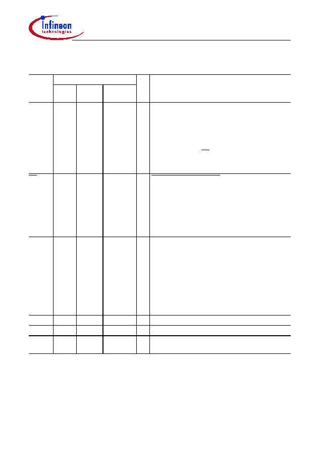
Table 1
Pin Definitions and Functions
Symbol Pin Number
I/O
*)
Function
P- DIP
-40
P-LCC-
44
P-MQFP-
44
P1.7-
P1.0
8-1
1
2
3
4
5
6
9-2
2
3
4
5
6
7
3-1,
44-40
40
41
42
43
44
1
I/O Port 1
Port 1 is an 8-bit quasi-bidirectional port with internal
pull-up arrangement. Port 1 pins that have "1s"
written to them are pulled high by the internal pull-up
transistors and in that state can be used as inputs.
As inputs, Port 1 pins being externally pulled low will
source current (
I
IL
, in the DC characteristics)
because of the internal pull-up transistors.
The output latch corresponding to a secondary
function must be programmed to 1 for that function
to operate.
For the outputs of the Synchronous Serial Channel
(SSC), SCLK and STO, special circuitry is
implemented providing true push-pull capability.
The STO output, in addition, will have true tristate
capability. When used for SSC inputs, the pull-up
transistors will be switched off and the inputs float
(high ohm inputs).
The secondary functions are assigned to the pins of
Port 1 as follows:
P1.0 / T2
Input to Counter 2
P1.1 / T2EX
Capture/reload trigger of Timer 2
Up-Down count
P1.2 / SCLK
SSC Master Clock Output
SSC Slave Clock Input
P1.3 / SRI
SSC Receive Input
P1.4 / STO
SSC Transmit Output
P1.5 / SLS
Slave Select Input
*)
I = Input
O = Output
c513ao_ds_0200.frm Page 7 Wednesday, August 30, 2000 12:45 PM

C513AO
Data Sheet
8
02.00
P3.0-
P.3.7
10-17
10
11
12
13
14
15
16
17
11,
13-19
11
13
14
15
16
17
18
19
5,
7-13
5
7
8
9
10
11
12
13
I/O Port 3
Port 3 is an 8-bit quasi-bidirectional port with internal
pull-up arrangement. Port 3 pins that have "1"s
written to them are pulled high by the internal pull-up
transistors and in that state can be used as inputs.
As inputs, Port 3 pins being externally pulled low will
source current (
I
IL
, in the DC characteristics)
because of the internal pull-up transistors.
The output latch corresponding to a secondary
function must be programmed to a "1" for that
function to operate (except for TxD and WR).
The secondary functions are assigned to the pins of
Port 3 as follows:
P3.0 / RxD
Receiver data input (asynch.)
or data input/output (synch.) of
serial interface
P3.1 / TxD
Transmitter data output
(asynch.) or clock output
(synch.) of serial interface
P3.2 / INT0
External Interrupt 0 input /
Timer 0 gate control input
P3.3 / INT1
External Interrupt 1 input /
Timer 1 gate control input
P3.4 / T0
Timer 0 counter input
P3.5 / T1
Timer 1 counter input
P3.6 / WR
WR control output; latches the
data byte from Port 0 into the
external data memory
P3.7 / RD
RD control output; enables the
external data memory to Port 0
RESET
9
10
4
I
RESET
A high level on this pin for the duration of two
machine cycles while the oscillator is running resets
the device. An internal diffused resistor to
V
SS
permits power-on reset using only an external
capacitor to
V
DD
.
*)
I = Input
O = Output
Table 1
Pin Definitions and Functions (cont'd)
Symbol Pin Number
I/O
*)
Function
P- DIP
-40
P-LCC-
44
P-MQFP-
44
c513ao_ds_0200.frm Page 8 Wednesday, August 30, 2000 12:45 PM

C513AO
Data Sheet
9
02.00
XTAL2
18
20
14
O
XTAL2
Output of the inverting oscillator amplifier.
XTAL1
19
21
15
I
XTAL1
Input to the inverting oscillator amplifier and input to
the internal clock generator circuits.
To drive the device from an external clock source,
XTAL1 should be driven, while XTAL2 is left
unconnected.
There
are no requirements on the
duty
cycle of the external clock signal, since the
input to the internal clocking circuitry is divided down
by a divide-by-two flip-flop. Minimum and maximum
high and low times as well as rise/fall times specified
in the AC characteristics must be observed.
P2.0-
P2.7
21-28
24-31
18-25
I/O Port 2
Port 2 is a an 8-bit quasi-bidirectional I/O port with
internal pull-up arrangement. Port 2 pins that have
"1s" written to them are pulled high by the internal
pull-up transistors, and in that state can be used as
inputs. As inputs, Port 2 pins being externally pulled
low will source current (
I
IL
, in the DC characteristics)
because of the internal pullup transistors. Port 2
emits the high-order address byte during fetches
from external program memory and during
accesses to external data memory that use 16-bit
addresses (MOVX @DPTR). In this application it
uses strong internal pullup transistors when issuing
"1"s. During accesses to external data memory that
use 8-bit addresses (MOVX @Ri), Port 2 issues the
contents of the P2 Special Function Register and
uses only the internal pull-up transistors.
PSEN
29
32
26
O
Program Store Enable
This is a control signal that enables output of the
external program memory to the bus during external
fetch operations. It is activated every three oscillator
periods except during external data memory
accesses. It remains high during internal program
execution.
This pin should not be driven during reset operation.
*)
I = Input
O = Output
Table 1
Pin Definitions and Functions (cont'd)
Symbol Pin Number
I/O
*)
Function
P- DIP
-40
P-LCC-
44
P-MQFP-
44
c513ao_ds_0200.frm Page 9 Wednesday, August 30, 2000 12:45 PM
C513AO
Data Sheet
10
02.00
ALE
30
33
27
O
Address Latch Enable
This output is used for latching the low-byte of the
address into external memory during normal
operation. It is activated every six oscillator periods
except during an external data memory access.
When instructions are executed from internal
program memory (EA = 1) the ALE generation can
be disabled by bit EALE in SFR SYSCON.
This pin should not be driven during reset operation.
EA
31
35
29
I
External Access Enable
When held at high level, instructions are fetched
from the internal program memory when the PC is
less than 4000
H
. When held at low level, the
C513AO fetches all instructions from external
program memory.
This pin should not be driven during reset operation.
Note: For the C513AO-L this pin must be tied low.
P0.0-
P0.7
32-39
43-36
37-30
I/O Port 0
Port 0 is an 8-bit open-drain bidirectional I/O port.
Port 0 pins that have "1s" written to them float, and
in that state can be used as high-impendance inputs.
Port 0 is also the multiplexed low-order address and
data bus during accesses to external program or
data memory. In this application, it uses strong
internal pull-up transistors when issuing 1s. External
pull-up resistors are required during program
verification.
V
SS
20
22, 1
16, 39
�
Ground (0 V)
V
DD
40
44, 23
38, 17
�
Power Supply (+ 5 V)
N.C.
�
12, 34
6, 28
�
No Connection. These pins should not be
connected.
*)
I = Input
O = Output
Table 1
Pin Definitions and Functions (cont'd)
Symbol Pin Number
I/O
*)
Function
P- DIP
-40
P-LCC-
44
P-MQFP-
44
c513ao_ds_0200.frm Page 10 Wednesday, August 30, 2000 12:45 PM

C513AO
Data Sheet
11
02.00
Figure 6
Block Diagram of the C513AO
MCB04011
Oscillator
Watchdog
OSC & Timing
CPU
Timer 0
Timer 1
Timer 2
Interrupt Unit
USART
SSC
XRAM
256 byte
RAM
256 byte
ROM/OTP
16 K x 8
Port 0
Port 1
Port 2
Port 3
Emulation
Support
Logic
Port 0
8-Bit
Digital I/O
C513AO
V
DD
V
SS
XTAL1
XTAL2
RESET
ALE
PSEN
EA
Port 1
8-Bit
Digital I/O
Port 2
8-Bit
Digital I/O
Port 3
8-Bit
Digital I/O
c513ao_ds_0200.frm Page 11 Wednesday, August 30, 2000 12:45 PM
C513AO
Data Sheet
12
02.00
CPU
The C513AO is efficient both as a controller and as an arithmetic processor. It has extensive
facilities for binary and BCD arithmetic and excels in its bit-handling capabilities. Efficient use of
program memory results from an instruction set consisting of 44% one-byte, 41% two-byte, and
15% three-byte instructions. With a 16-MHz crystal, 58% of the instructions execute in 750 ns.
Special Function Register PSW (Address D0
H
)
Reset Value: 00
H
Bit
Function
CY
Carry Flag
Used by arithmetic instruction.
AC
Auxiliary Carry Flag
Used by instructions which execute BCD operations.
F0
General Purpose Flag 0
RS1
RS0
Register bank Select control bits
These bits are used to select one of the four register banks.
OV
Overflow Flag
Used by arithmetic instruction.
F1
General Purpose Flag 1
P
Parity Flag
Set/cleared by hardware after each instruction to indicate an odd/even
number of "one" bits in the accumulator, i.e. even parity.
CY
AC
F0
RS1
RS0
OV
F1
P
D0
H
PSW
D7
H
D6
H
D5
H
D4
H
D3
H
D2
H
D1
H
D0
H
Bit No.
MSB
LSB
RS1
RS0
Function
0
0
Bank 0 selected, data address 00
H
-07
H
0
1
Bank 1 selected, data address 08
H
-0F
H
1
0
Bank 2 selected, data address 10
H
-17
H
1
1
Bank 3 selected, data address 18
H
-1F
H
c513ao_ds_0200.frm Page 12 Wednesday, August 30, 2000 12:45 PM

C513AO
Data Sheet
13
02.00
Memory Organization
The C513AO CPU manipulates operands in the following five address spaces:
� Up to 64 Kbytes of program memory (up to 16 KB on-chip program memory for the C513AO-2R/
2E)
� Up to 64 Kbytes of external data memory
� 256 bytes of internal data memory
� 256 bytes of internal XRAM data memory
� One 128-byte special function register area
Figure 7 illustrates the memory address spaces of the C513AO.
Figure 7
C513AO Memory Map
MCA04012
Special
Function
Regs.
FF
H
80
H
Direct
Addr.
Indirect
Addr.
80
H
FF
H
Internal
RAM
00
H
7F
H
Internal
RAM
"Internal Data Space"
Internal
XRAM
(256 byte)
FFFF
H
FF00
H
Ext.
Data
Memory
0000
H
FEFF
H
Ext.
Data
Memory
"Data Space"
4000
H
FFFF
H
Ext.
"Code Space"
Ext.
(EA = 0)
3FFF
H
0000
H
Int.
(EA = 1)
c513ao_ds_0200.frm Page 13 Wednesday, August 30, 2000 12:45 PM

C513AO
Data Sheet
14
02.00
Reset and System Clock
The reset input is an active high input. An internal Schmitt-trigger is used at the input for noise
rejection. Since the reset is synchronized internally, the RESET pin must be held high for at least
two machine cycles (24 oscillator periods) while the oscillator is running. With the oscillator running,
the internal reset is executed during the second machine cycle and is repeated every cycle until
RESET goes low again. Figure 8 shows the possible reset circuitries.
Figure 8
Reset Circuitries
C513AO
RESET
V
DD
+
C513AO
RESET
C513AO
RESET
&
+
V
DD
a)
b)
c)
MCS03291
c513ao_ds_0200.frm Page 14 Wednesday, August 30, 2000 12:45 PM

C513AO
Data Sheet
15
02.00
Figure 9 shows the recommended oscillator circiutries for crystal and external clock operation.
Figure 9
Recommended Oscillator Circuitry
In this application, the on-chip oscillator is used as a crystal-controlled, positive-reactance oscillator
(a more detailed schematic is given in Figure 10). lt is operated in its fundamental response mode
as an inductive reactor in parallel resonance with a capacitor external to the chip. The crystal
specifications and capacitances are non-critical. In this circuit, 20 pF can be used as single
capacitance at any frequency together with a good quality crystal. A ceramic resonator can be used
in place of the crystal in cost-critical applications. If a ceramic resonator is used, the two capacitors
normally will have different values, dependent on the oscillator frequency. We recommend
consulting the manufacturer of the ceramic resonator for value specifications of these capacitors.
MCS04014
XTAL2
C513AO
XTAL1
3.5-16 MHz
C
C
C
= 20 pF �10 pF for crystal operation
c513ao_ds_0200.frm Page 15 Wednesday, August 30, 2000 12:45 PM

C513AO
Data Sheet
16
02.00
Figure 10
On-Chip Oscillator Circuitry
To drive the C513AO with an external clock source, the external clock signal must be applied to
XTAL1, as shown in Figure 11. XTAL2 must be left unconnected. A pull-up resistor is suggested to
increase the noise margin, but is optional if
V
OH
of the driving gate corresponds to the
V
IH2
specification of XTAL1.
Figure 11
External Clock Source
MCS04015
C513AO
To internal
timing circuitry
**
)
*
)
XTAL2
XTAL1
Crystal or ceramic resonator
Resistor is only in the C513AO-2E
*
)
**
)
C
1
C
2
MCS04016
V
DD
External
Clock
Signal
C513AO
XTAL2
XTAL1
N.C.
c513ao_ds_0200.frm Page 16 Wednesday, August 30, 2000 12:45 PM
C513AO
Data Sheet
17
02.00
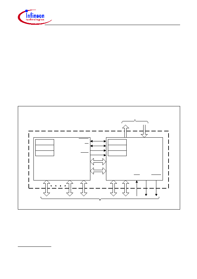
Enhanced Hooks Emulation Concept
The Enhanced Hooks Emulation Concept of the C500 microcontroller family is a new, innovative
way to control the execution of C500 MCUs and to gain extensive information on the internal
operation of the controllers. Emulation of on-chip ROM based programs is possible, too.
Each production chip has built-in logic for the support of the Enhanced Hooks Emulation Concept.
Therefore, no costly bond-out chips are necessary for emulation. This also ensure that emulation
and production chips are identical.
The Enhanced Hooks Technology
TM
1)
, which requires embedded logic in the C500 allows the C500
together with an EH-IC to function similar to a bond-out chip. This simplifies the design and reduces
costs of an ICE-system. ICE-systems using an EH-IC and a compatible C500 are able to emulate
all operating modes of the different versions of the C500 microcontrollers. This includes emulation
of ROM, ROM with code rollover and ROMless modes of operation. It is also able to operate in
single step mode and to read the SFRs after a break.
Figure 12
Basic C500 MCU Enhanced Hooks Concept Configuration
Port 0, port 2 and some of the control lines of the C500 based MCU are used by Enhanced Hooks
Emulation Concept to control the operation of the device during emulation and to transfer
informations about the program execution and data transfer between the external emulation
hardware (ICE-system) and the C500 MCU.
1 "Enhanced Hooks Technology" is a trademark and patent of Metalink Corporation licensed to Infineon
Technologies.
SYSCON
PCON
TCON
RESET
EA
ALE
PSEN
Port 0
Port 2
Port 1
Port 3
opt.
I/O Ports
C500
MCU
2
RPCON
RTCON
Enhanced Hooks
Interface Circuit
RSYSCON
0
RPORT RPORT
TEA TALE TPSEN
EH-IC
ICE-System interface
to emulation hardware
Target System Interface
MCS03254
c513ao_ds_0200.frm Page 17 Wednesday, August 30, 2000 12:45 PM

C513AO
Data Sheet
18
02.00
Special Function Registers
The registers reside in the special function register area, with the exception of the Program Counter
and the four General Purpose Register banks. The special function register area consists of two
portions: the
standard
special function register area and the
mapped
special function register area.
Four special function registers of the C513AO (PCON1, VR0, VR1 & VR2) are located in the
mapped special function register area. For accessing the mapped special function register area, bit
RMAP in special function register SYSCON must be set. All other special function registers of the
C513AO are located in the standard special function register area.
Special Function Register SYSCON (Address B1
H
)
Reset Value: XX10XXX0
B
If bit RMAP is set, mapped special function registers can be accessed. This bit is not cleared by
hardware automatically.
The forty Special Function Registers (SFRs) in the standard and mapped SFR area include pointers
and registers that provide an interface between the CPU and the other on-chip peripherals. The
SFRs of the C513AO are listed in Table 2 and Table 3. In Table 2, they are organized in groups
which refer to the functional blocks of the C513AO. Table 3 illustrates the contents of the SFRs in
numeric order of their addresses.
Bit
Function
RMAP
Special function Register MAP bit
RMAP = 0: The access to the non-mapped (standard) special function
register area is enabled.
RMAP = 1: The access to the mapped special function register area is
enabled.
�
Reserved bits for future use. Read by CPU returns undefined values.
7
6
5
4
3
2
1
0
EALE
RMAP
�
B1
H
SYSCON
Bit No.
MSB
LSB
�
�
�
XMAP
The functions of the shaded bits are not described in this section.
�
c513ao_ds_0200.frm Page 18 Wednesday, August 30, 2000 12:45 PM

C513AO
Data Sheet
19
02.00
Table 2
Special Function Registers - Functional Blocks
Block
Symbol
Name
Address Contents after
Reset
CPU
ACC
B
DPH
DPL
PSW
SP
SYSCON
2)
VR0
4) 5)
VR1
4) 5)
VR2
4) 5)
Accumulator
B-Register
Data Pointer, High Byte
Data Pointer, Low Byte
Program Status Word Register
Stack Pointer
System Control Register
Version Register 0
Version Register 1
6)
Version Register 2
7)
E0
H
1)
F0
H
1)
83
H
82
H
D0
H
1)
81
H
B1
H
FC
H
FD
H
FE
H
00
H
00
H
00
H
00
H
00
H
07
H
XX10XXX0
B
3)
C5
H
�
�
Interrupt
System
IE
IP
Interrupt Enable Register
Interrupt Priority Register
A8
H
1)
B8
H
1)
00
H
X0000000
B
3)
Ports
P0
P1
P2
P3
Port 0
Port 1
Port 2
Port 3
80
H
1)
90
H
1)
A0
H
1)
B0
H
1)
FF
H
FF
H
FF
H
FF
H
Serial
Channel
(USART)
PCON
2)
SBUF
SCON
Power Control Register
Serial Channel Buffer Register
Serial Channel Control Register
87
H
99
H
98
H
1)
000X0000
B
XX
H
3)
00
H
SSC
Interface
SSCCON
STB
SRB
SCF
SCIEN
SSCMOD
8)
SSC Control Register
SSC Transmit Register
SSC Receive Register
SSC Flag Register
SSC Interrupt Enable Register
SSC Mode Test Register
E8
H
1)
E9
H
EA
H
F8
H
1)
F9
H
EB
H
07
H
XX
H
3)
XX
H
3)
XXXXXX00
B
3)
XXXXXX00
B
3)
00
H
Timer 0/
Timer 1
TCON
TH0
TH1
TL0
TL1
TMOD
Timer 0/1 Control Register
Timer 0, High Byte
Timer 1, High Byte
Timer 0, Low Byte
Timer 1, Low Byte
Timer Mode Register
88
H
1)
8C
H
8D
H
8A
H
8B
H
89
H
00
H
00
H
00
H
00
H
00
H
00
H
1) Bit-addressable special function registers
2) This special function register is listed repeatedly since some bits of it also belong to other functional blocks.
3) "X" means that the value is undefined and the location is reserved
4) This SFR is a mapped SFR area. For accessing this SFR, bit RMAP in SFR SYSCON must be set.
5) This SFR is read-only.
6) C513AO-L/2R: 13
H
C513AO-2E: 83
H
7) This SFR varies with the step of the microcontroller: for example, 01
H
for the first step
8) This register is only used for test purposes and must not be written during normal operation. Unpredictable
results may occur upon a write operation.
c513ao_ds_0200.frm Page 19 Wednesday, August 30, 2000 12:45 PM

C513AO
Data Sheet
20
02.00
Timer 2
T2CON
T2MOD
RC2H
RC2L
TH2
TL2
Timer 2 Control Register
Timer 2 Mode Register
Timer 2 Reload/Capture Register, High Byte
Timer 2 Reload/Capture Register, Low Byte
Timer 2 High Byte
Timer 2 Low Byte
C8
H
1)
C9
H
CB
H
CA
H
CD
H
CC
H
00
H
XXXXXXX0
B
3)
00
H
00
H
00
H
00
H
Watchdog WDCON
WDTREL
Watchdog Timer Control Register
Watchdog Timer Reload Register
C0
H
1)
86
H
XXXX0000
B
3)
00
H
Power
Save
Mode
PCON
2)
PCON1
4)
Power Control Register
Power Control Register 1
87
H
88
H
000X0000
B
3)
0XXXXXXX
B
3)
1) Bit-addressable special function registers
2) This special function register is listed repeatedly since some bits of it also belong to other functional blocks.
3) "X" means that the value is undefined and the location is reserved
4) This SFR is a mapped SFR area. For accessing this SFR, bit RMAP in SFR SYSCON must be set.
5) This SFR is read-only.
6) C513AO-L/2R: 13
H
C513AO-2E: 83
H
7) This SFR varies with the step of the microcontroller: for example, 01
H
for the first step
8) This register is only used for test purposes and must not be written during normal operation. Unpredictable
results may occur upon a write operation.
Table 2
Special Function Registers - Functional Blocks (cont'd)
Block
Symbol
Name
Address Contents after
Reset
c513ao_ds_0200.frm Page 20 Wednesday, August 30, 2000 12:45 PM
C513AO
Data Sheet
21
02.00
Table 3
Contents of the SFRs, SFRs in Numeric Order of their Addresses
Addr.
Register
Content
after
Reset
1)
Bit 7
Bit 6
Bit 5
Bit 4
Bit 3
Bit 2
Bit 1
Bit 0
80
H
2)
P0
FF
H
.7
.6
.5
.4
.3
.2
.1
.0
81
H
SP
07
H
.7
.6
.5
.4
.3
.2
.1
.0
82
H
DPL
00
H
.7
.6
.5
.4
.3
.2
.1
.0
83
H
DPH
00
H
.7
.6
.5
.4
.3
.2
.1
.0
86
H
WDTREL 00
H
WDT
PSEL
.6
.5
.4
.3
.2
.1
.0
87
H
PCON
0XX0-
0000
B
SMOD
�
�
SD
GF1
GF0
PDE
IDLE
88
H
2) 3)
TCON
00
H
TF1
TR1
TF0
TR0
IE1
IT1
IE0
IT0
88
H
3)
PCON1
0XX0-
XXXX
B
EWPD
�
�
�
�
�
�
�
89
H
TMOD
00
H
GATE
C/T
M1
M0
GATE
C/T
M1
M0
8A
H
TL0
00
H
.7
.6
.5
.4
.3
.2
.1
.0
8B
H
TL1
00
H
.7
.6
.5
.4
.3
.2
.1
.0
8C
H
TH0
00
H
.7
.6
.5
.4
.3
.2
.1
.0
8D
H
TH1
00
H
.7
.6
.5
.4
.3
.2
.1
.0
90
H
2)
P1
FF
H
�
�
.SLS
STO
SRI
SCLK
T2EX
T2
98
H
2)
SCON
00
H
SM0
SM1
SM2
REN
TB8
RB8
TI
RI
99
H
SBUF
XX
H
.7
.6
.5
.4
.3
.2
.1
.0
A0
H
2)
P2
FF
H
.7
.6
.5
.4
.3
.2
.1
.0
A8
H
2)
IE
00
H
EA
ESSC ET2
ES
ET1
EX1
ET0
EX0
B0
H
2)
P3
FF
H
RD
WR
T1
T0
INT1
INT0
TxD
RxD
B1
H
SYSCON XX10-
XXX0
B
�
�
EALE RMAP
�
�
�
XMAP
B8
H
2)
IP
X000-
0000
B
�
PSSC PT2
PS
PT1
PX1
PT0
PX0
C0
H
2)
WDCON
XXXX-
0000
B
�
�
�
�
OWDS WDTS WDT
SWDT
1) "X" means that the value is undefined and the location is reserved.
2) Bit-addressable special function registers.
3) SFR is located in the mapped SFR area. For accessing this SFR, bit RMAP in SFR SYSCON must be set.
4) These are read-only registers.
5) The content of this SFR varies with the actual step of the C513A0: for example, 01
H
for the first step).
6) This register is only used for test purposes and must not be written during normal operation. Unpredictable
results may occur upon a write operation.
c513ao_ds_0200.frm Page 21 Wednesday, August 30, 2000 12:45 PM

C513AO
Data Sheet
22
02.00
C8
H
2)
T2CON
00
H
TF2
EXF2 RCLK TCLK
EXEN2 TR2
C/T2
CP/
RL2
C9
H
T2MOD
XXXX-
XXX0
B
�
�
�
�
�
�
�
DCEN
CA
H
RC2L
00
H
.7
.6
.5
.4
.3
.2
.1
.0
CB
H
RC2H
00
H
.7
.6
.5
.4
.3
.2
.1
.0
CC
H
TL2
00
H
.7
.6
.5
.4
.3
.2
.1
.0
CD
H
TH2
00
H
.7
.6
.5
.4
.3
.2
.1
.0
D0
H
2)
PSW
00
H
CY
AC
F0
RS1
RS0
OV
F1
P
E0
H
2)
ACC
00
H
.7
.6
.5
.4
.3
.2
.1
.0
E8
H
2)
SSCCON 07
H
SCEN
TEN
MSTR CPOL
CPHA
BRS2
BRS1
BRS0
E9
H
STB
XX
H
.7
.6
.5
.4
.3
.2
.1
.0
EA
H
SRB
XX
H
.7
.6
.5
.4
.3
.2
.1
.0
EB
H
SSCMOD 00
H
6)
LOOPB TRIO
0
0
0
0
0
LSBSM
F0
H
2)
B
00
H
.7
.6
.5
.4
.3
.2
.1
.0
F8
H
2)
SCF
XXXX-
XX00
B
�
�
�
�
�
�
WCOL
TC
F9
H
SCIEN
XXXX-
XX00
B
�
�
�
�
�
�
WCEN
TCEN
FC
H
3) 4)
VR0
C5
H
.7
.6
.5
.4
.3
.2
.1
.0
FD
H
3) 4)
VR1
�
7)
.7
.6
.5
.4
.3
.2
.1
.0
FE
H
3) 4)
VR2
�
5)
.7
.6
.5
.4
.3
.2
.1
.0
1) "X" means that the value is undefined and the location is reserved
2) Bit-addressable special function registers
3) SFR is located in the mapped SFR area. For accessing this SFR, bit RMAP in SFR SYSCON must be set.
4) These SFRs are read-only registers.
5) The content of this SFR varies with the actual step of the C513A0: for example, 01
H
for the first step)
6) This register is only used for test purposes and must not be written during normal operation. Unpredictable
results may occur upon a write operation.
7) C513AO-L/2R: 13
H
C513AO-2E: 83
H
Table 3
Contents of the SFRs, SFRs in Numeric Order of their Addresses (cont'd)
Addr.
Register
Content
after
Reset
1)
Bit 7
Bit 6
Bit 5
Bit 4
Bit 3
Bit 2
Bit 1
Bit 0
c513ao_ds_0200.frm Page 22 Wednesday, August 30, 2000 12:45 PM

C513AO
Data Sheet
23
02.00
Parallel I/O Port
The C513AO has four 8-bit I/O ports. Port 0 is an open-drain bidirectional I/O port, while Ports 1, 2,
and 3 are quasi-bidirectional I/O ports with internal pull-up resistors. Thus, when configured as
inputs, Ports 1 to 3 will be pulled high and will source current when externally pulled low. Port 0 will
float when configured as input.
The output drivers of Port 0 and Port 2 and the input buffers of Port 0 are also used for accessing
external memory. In this application, Port 0 outputs the low byte of the external memory address,
time multiplexed with the byte being written or read. Port 2 outputs the high byte of the external
memory address when the address is 16 bits wide. Otherwise, the Port 2 pins continue to emit the
P2 SFR contents. In this case, Port 0 is not an open-drain port, but uses a strong internal pull-up
Field Effect Transistors (FETs).
Port 1 pins used for Synchronous Serial Channel (SSC) outputs are true push-pull outputs. When
used as SSC inputs, they float (no pull-up).
c513ao_ds_0200.frm Page 23 Wednesday, August 30, 2000 12:45 PM

C513AO
Data Sheet
24
02.00
Timer/Counter 0 and 1
Timer/Counter 0 and 1 can be used in four operating modes as listed in Table 4:
In the "timer" function (C/T = `0') the register is incremented every machine cycle. Since a machine
cycle consists of twelve oscillator periods, the count rate is 1/12th of the oscillator frequency.
In "counter" function, the register is incremented in response to a 1-to-0 transition (falling edge) at
its corresponding external input pin, T0 or T1 (alternate functions of P3.4 and P3.5, respectively).
Since it takes two machine cycles to detect a falling edge; therefore, the maximum count rate is 1/
24th of the oscillator frequency. External inputs INT0 and INT1 (P3.2, P3.3) can be programmed to
function as a gate to facilitate pulse width measurements. Figure 13 illustrates the input clock logic.
Figure 13
Timer/Counter 0 and 1 Input Clock Logic
Table 4
Timer/Counter 0 and 1 Operating Modes
Mode
Description
TMOD
Input Clock
M1
M0
Internal
External (max.)
0
8-bit timer/counter with a
divide-by-32 prescaler
0
0
f
OSC
/(12
�
32)
f
OSC
/(24
�
32)
1
16-bit timer/counter
1
1
f
OSC
/12
f
OSC
/24
2
8-bit timer/counter with
8-bit autoreload
1
0
3
Timer/counter 0 used as one
8-bit timer/counter and one
8-bit timer
Timer 1 stops
1
1
�
12
12
f
OSC
/12
MCS01768
OSC
f
C/T
TMOD
0
Control
Timer 0/1
Input Clock
TCON
TR 0/1
Gate
TMOD
&
=1
1
P3.4/T0
P3.5/T1
max
P3.2/INT0
P3.3/INT1
OSC
/24
f
1
�
_
<
c513ao_ds_0200.frm Page 24 Wednesday, August 30, 2000 12:45 PM

C513AO
Data Sheet
25
02.00
Timer/Counter 2 with Compare/Capture/Reload
Timer 2 is a 16-bit timer/counter with an up/down count feature. It has three operating modes:
� 16-bit auto-reload mode (up or down counting)
� 16-bit capture mode
� Baudrate generator
Note:
denotes a falling edge
Table 5
Timer / Counter 2 Operating Modes
Mode
T2CON
T2MOD T2CON
P1.1/
T2EX
Remarks
Input Clock
RCLK
or
TCLK
CP/
RL2
TR2
DCEN
EXEN2
Internal
External
(P1.0/
T2)
16-bit
Auto-
reload
0
0
0
0
0
0
0
0
1
1
1
1
0
0
1
1
0
1
X
X
X
0
1
reload upon
overflow
reload trigger
(falling edge)
down counting
up counting
f
OSC
/12
max
f
OSC
/24
16-bit
Capture
0
0
1
1
1
1
X
X
0
1
X
16-bit Timer/
Counter (only
up-counting)
capture TH2,
TL2
RC2H,
RC2L
f
OSC
/12
max
f
OSC
/24
Baudrate
Generator
1
1
X
X
1
1
X
X
0
1
X
no overflow
interrupt
request (TF2)
extra external
interrupt
("Timer 2")
f
OSC
/12
max
f
OSC
/24
off
X
X
0
X
X
X
Timer 2 stops
�
�
c513ao_ds_0200.frm Page 25 Wednesday, August 30, 2000 12:45 PM

C513AO
Data Sheet
26
02.00
Serial Interface (USART)
The serial port is a full duplex port capable of simultaneous transmit and receive functions. It is also
receive-buffered; it can commence reception of a second byte before a previously-received byte
has been read from the receive register. The serial port can operate in 4 modes (one synchronous
and three asynchronous) as illustrated in Table 6.
For clarification, some terms regarding the difference between "baudrate clock" and "baudrate"
should be mentioned.
The serial interface requires a clock rate which is 16 times the baudrate for internal synchronization.
Therefore, the baudrate generators must provide a "baudrate clock" to the serial interface which
divides it by 16, thereby resulting in the actual "baudrate".
The baudrates in Mode 1 and 3 are determined by the timer overflow rate. These baudrates can be
determined by Timer 1 or by Timer 2 or both (one for transmit, the other for receive).
Table 6
USART Operating Modes
Mode
SCON
Description
SM0
SM1
0
0
0
Shift register mode
Serial data enters and exits through R
�
D. T
�
D outputs the
shift clock. 8-bit data are transmitted/received (LSB first) at a
fixed baudrate of
1
/
12
th of the oscillator frequency.
1
0
1
8-bit USART, variable baudrate
10 bits are transmitted (through T
�
D) or received (at R
�
D).
2
1
0
9-bit USART, fixed baudrate
11 bits are transmitted (through T
�
D) or received (at R
�
D).
3
1
1
9-bit USART, variable baudrate
Similar to mode 2, except for the variable baudrate.
c513ao_ds_0200.frm Page 26 Wednesday, August 30, 2000 12:45 PM

C513AO
Data Sheet
27
02.00
Figure 14
Block Diagram of Baudrate Generation for the Serial Interface
Table 7 lists the values/formulas for the baudrate calculation of the serial interface with its
dependencies on the control bits SMOD (in SFR PCON), TCLK and RCLK (both in SFR T2CON).
Table 7
Serial Interface - Baudrate Dependencies
Serial Interface
Operating Modes
Control Bits
Baudrate Calculation
SMOD
TCLK/RCLK
Mode 0 (Shift Register)
�
�
f
OSC
/12
Mode 1 (8-bit UART)
Mode 3 (9-bit UART)
X
0
Determined by timer 1 overflow rate:
(2
SMOD
�
timer 1 overflow rate)/32
�
1
Determined by timer 2 overflow rate:
Timer 2 overflow rate/16
Mode 2 (9-bit UART)
0
1
�
�
f
OSC
/64
f
OSC
/32
MCS04017
SCON.7/
SCON.6
(SM0/
SM1)
Mode 1
Mode 3
Mode 2
Mode 0
� 6
f
OSC
/2
Timer 1 Overflow
Only one mode
can be selected
PCON.7
(SMOD)
� 2
Baudrate
Clock
0
1
Note: The switch configuration shows the reset state
c513ao_ds_0200.frm Page 27 Wednesday, August 30, 2000 12:45 PM

C513AO
Data Sheet
28
02.00
SSC Interface
The Synchronous Serial Channel (SSC) interface is compatible to the popular SPI serial bus
interface. It can be used for simple I/O expansion via shift registers, for connection with a variety of
peripheral components (such as A/D converters, EEPROMs etc.), or interconnection of several
microcontrollers in a master/slave structure. The SSC unit supports full-duplex or half-duplex
operation and can run in Master Mode or Slave Mode.
Figure 15 shows the block diagram of the SSC.
Figure 15
SSC Block Diagram
Interrupt System
The C513AO provides seven interrupt sources with two priority levels. Five of the interrupts can be
generated by the on-chip peripherals (Timer 0, Timer 1, Timer 2, USART, and SSC) and three of the
interrupts may be triggered externally (P1.1/T2EX, P3.2/INT0, P3.3/INT1). A non-maskable eighth
interrupt is reserved for external wake-up from power-down mode.
Figure 16 gives a general overview of the interrupt sources and illustrates the request and the
control flags. Table 8 lists the vector addresses of each interrupt source.
MCB02735
P1.2/SCLK
P1.3/SRI
P1.4/STO
P1.5/SLS
Pin
Control
Logic
Shift Register
Receive Buffer Register
STB
Clock Selection
Clock Divider
SRB
f
OSC
Control Register
Status Register
Int. Enable Reg.
SCIEN
SSCCON
SCF
Control Logic
Internal Bus
Interrupt
c513ao_ds_0200.frm Page 28 Wednesday, August 30, 2000 12:45 PM

C513AO
Data Sheet
29
02.00
Figure 16
Interrupt Request Sources
c513ao_ds_0200.frm Page 29 Wednesday, August 30, 2000 12:45 PM

C513AO
Data Sheet
30
02.00
If two interrupt requests of different priority levels are received simultaneously, the request of higher
priority is serviced. If requests of the same priority are received simultaneously, an internal polling
sequence determines which request is serviced. Thus, within each priority level there is a second
priority structure determined by the polling sequence as shown in Table 9.
A low-priority interrupt can be interrupted by a high-priority interrupt, but not by another low-priority
interrupt. A high-priority interrupt cannot be interrupted by any other interrupt source.
Table 8
Interrupt Vector Addresses
Interrupt Source
Request Flags
Vector Address
External interrupt 0
Timer 0 interrupt
External interrupt 1
Timer 1 interrupt
USART serial port interrupt
Timer 2 interrupt
Synchronous Serial Channel interrupt (SSC)
Wake-up from power-down mode
IE0
TF0
IE1
TF1
RI + TI
TF2 + EXF2
WCOL+TC
�
0003
H
000B
H
0013
H
001B
H
0023
H
002B
H
0043
H
007B
H
Table 9
Interrupt Source Structure
Interrupt Source
Priority
External Interrupt 0
Synchronous Serial Channel
Timer 0 Interrupt
External Interrupt 1
Timer 1 Interrupt
Universal Serial Channel
Timer 2 Interrupt
IE0
WCOL OR TC
TFO
IE1
TF1
RI OR TI
TF2 OR EXF2
High
Low
c513ao_ds_0200.frm Page 30 Wednesday, August 30, 2000 12:45 PM

C513AO
Data Sheet
31
02.00
Fail Save Mechanisms
The C513AO offers enhanced fail-safe mechanisms which allow automatic recovery from a
software upset or a hardware failure:
� A programmable Watchdog Timer (WDT) has variable time-out period from 512
�
s up to approx.
1.1 sec. at 12 MHz
� An Oscillator Watchdog (OWD) monitors the on-chip oscillator and forces the microcontroller into
reset state if the on-chip oscillator fails. It also provides the clock for a fast internal reset after
power-on.
The Watchdog Timer in the C513AO is a 15-bit timer which is incremented by a count rate of either
f
CYCLE
/2 or
f
CYCLE
/32 (
f
CYCLE
=
f
OSC
/12). That is, the machine clock is divided by a fixed divide-by-two
prescaler and an optional divide-by-16 prescaler arranged in series. For programming of the
watchdog timer overflow rate, the upper 7 bit of the watchdog timer can be written. Figure 17 shows
the block diagram of the watchdog timer unit.
Figure 17
Block Diagram of the Watchdog Timer
The Watchdog Timer can be started by software (bit SWDT in SFR WDCON); but, it cannot be
stopped during active mode of the device. If the software fails to clear the Watchdog Timer, an
internal reset will be initiated. The reset cause can be examined by software (status flag WDTS in
WDCON is set). A refresh of the Watchdog Timer is done by setting bits WDT (SFR WDCON) and
SWDT consecutively. This double instruction sequence has been implemented to increase system
security. During a refresh, the content of the SFR WDTREL is transferred to SFR WDTH, i.e. the
upper 7-bit of the watchdog timer. It must be noted, however, that the watchdog timer is stopped
during the idle mode and power down mode of the processor.
c513ao_ds_0200.frm Page 31 Wednesday, August 30, 2000 12:45 PM

C513AO
Data Sheet
32
02.00
Oscillator Watchdog
The Oscillator Watchdog (OWD) unit is used for three functions:
� Monitoring the on-chip oscillator's function
The watchdog supervises the on-chip oscillator's frequency. If the frequency is lower than the
frequency of the auxiliary RC oscillator in the watchdog unit, the internal clock is supplied by the
RC oscillator and the device is brought into reset. If the failure condition disappears (that is, if the
on-chip oscillator has a higher frequency than the RC oscillator), the device executes a final reset
phase of typically 1 ms to allow the oscillator to stabilize. Then, the oscillator watchdog reset is
released and the device resumes program execution.
� Fast internal reset after power-on
The oscillator watchdog unit provides a clock supply for reset before the on-chip oscillator has
started. The oscillator watchdog unit reset works identically to the monitoring function.
� Control of external wake-up from software power-down mode
When power-down mode is terminated by a low level at the INT0 pin, the oscillator watchdog unit
ensures that the microcontroller resumes operation (execution of the power-down wake-up
interrupt) with the nominal clock rate. In power-down mode, the RC oscillator and the on-chip
oscillator are stopped. Both oscillators are started again when power-down mode is terminated.
When the on-chip oscillator has a frequency higher than the RC oscillator, the microcontroller
starts operation after a final delay of typ. 1 ms to allow the on-chip oscillator to stabilize.
Note: The Oscillator Watchdog unit is always enabled.
Figure 18 shows the block diagram of the Oscillator Watchdog unit.
c513ao_ds_0200.frm Page 32 Wednesday, August 30, 2000 12:45 PM

C513AO
Data Sheet
33
02.00
Figure 18
Block Diagram of the Oscillator Watchdog
c513ao_ds_0200.frm Page 33 Wednesday, August 30, 2000 12:45 PM

C513AO
Data Sheet
34
02.00
Power Saving Modes
The C513AO provides three basic power-saving modes: Idle Mode, Slow-down Mode, and Power-
down Mode.
� Idle mode
The CPU is gated off from the oscillator. All peripherals are still provided with the clock and are
able to function. Idle mode is entered by software and can be left by an interrupt or reset.
� Slow down mode
The controller keeps up the full operating functionality, but its normal clock frequency is internally
divided by 32. This slows down all parts of the controller, the CPU and all peripherals, to 1/32nd
of their normal operating frequency and also reduces power consumption.
� Power down mode
The operation of the C513AO is completely stopped and the oscillator is turned off. This mode is
used to save the contents of the internal RAM with a very low standby current. This power down
mode is entered by software and can be left by reset or a short low pulse at pin P3.2/INT0.
In the power down mode of operation,
V
DD
can be reduced to minimize power consumption. It must
be ensured, however, that
V
DD
is not reduced before the power down mode is invoked, and that
V
DD
is restored to its normal operating level, before the power down mode is terminated. Table 10 gives
a general overview of the entry and exit procedures of the power saving modes.
Table 10
Power Saving Modes Overview
Mode
Entering
Example
Leaving by
Remarks
Idle mode
ORL PCON, #01
H
Occurrence of an any
enabled interrupt
CPU clock is stopped;
CPU maintains their data;
peripheral units are active (if
enabled) and provided with clock
Hardware reset
Slow Down Mode
In normal mode:
ORL PCON,#10
H
ANL PCON,#0EF
H
or Hardware reset
Internal clock rate is reduced to
1/32 of its nominal frequency
With idle mode:
ORL PCON,#11
H
Occurrence of any
enabled interrupt and
the instruction
ANL PCON,#0EF
H
CPU clock is stopped;
CPU maintains their data;
peripheral units are active (if
enabled) and provided with 1/32
of its nominal frequency
Hardware reset
Power Down
Mode
ORL PCON, #02
H
Hardware reset
Oscillator is stopped;
contents of on-chip RAM and
SFRs are maintained;
Short low pulse at pin
P3.2/INT0
c513ao_ds_0200.frm Page 34 Wednesday, August 30, 2000 12:45 PM

C513AO
Data Sheet
35
02.00
Absolute Maximum Ratings
Note: Stresses above those listed under "Absolute Maximum Ratings" may cause permanent
damage of the device. This is a stress rating only and functional operation of the device at
these or any other conditions above those indicated in the operational sections of this
specification is not implied. Exposure to absolute maximum rating conditions for longer
periods may affect device reliability. During absolute maximum rating overload conditions
(
V
IN
>
V
DD
or
V
IN
<
V
SS
) the voltage on
V
DD
pins with respect to ground (
V
SS
) must not exceed
the values defined by the absolute maximum ratings.
Operating Conditions
Parameter
Symbol
Limit Values
Unit
Notes
min.
max.
Storage temperature
T
ST
� 65
150
� C
�
Voltage on
V
DD
pins with respect
to ground (
V
SS
)
V
DD
� 0.5
6.5
V
�
Voltage on any pin with respect
to ground (
V
SS
)
V
IN
� 0.5
V
DD
+ 0.5
V
�
Input current on any pin during
overload condition
�
� 10
10
mA
�
Absolute sum of all input currents
during overload condition
�
�
|100 mA|
mA
�
Power dissipation
P
DISS
�
t.b.d.
W
�
Parameter
Symbol
Limit Values
Unit
Notes
min.
max.
Supply voltage
V
DD
4.25
5.5
V
�
Ground voltage
V
SS
0
V
�
Ambient temperature
SAB-C513AO
SAF-C513AO
T
A
T
A
0
� 40
70
85
� C
�
CPU clock
f
CPU
3.5
16
MHz �
c513ao_ds_0200.frm Page 35 Wednesday, August 30, 2000 12:45 PM

C513AO
Data Sheet
36
02.00
Parameter Interpretation
The parameters listed in the following partly represent the characteristics of the C513AO and partly
its demands on the system. To aid in interpreting the parameters right, when evaluating them for a
design, they are marked in column "Symbol":
CC (Controller Characteristics):
The logic of the C513AO will provide signals with the respective characteristics.
SR (System Requirement):
The external system must provide signals with the respective characteristics to the C513AO.
DC Characteristics
(Operating Conditions apply)
Parameter
Symbol
Limit Values
Unit Test Condition
min.
max.
Input low voltage
Pins except EA, RESET
EA pin
RESET pin
V
IL
SR
V
IL1
SR
V
IL2
SR
� 0.5
� 0.5
� 0.5
0.2
V
DD
� 0.1
0.2
V
DD
� 0.3
0.2
V
DD
+ 0.1
V
V
V
�
�
�
Input high voltage
Pins except XTAL1, RESET
XTAL1 pin
RESET pin
V
IH
SR
V
IH1
SR
V
IH2
SR
0.6
V
DD
0.7
V
DD
0.6
V
DD
V
DD
+ 0.5
V
DD
+ 0.5
V
DD
+ 0.5
V
V
V
�
�
�
Output low voltage
Ports 1, 2, 3 (except P1.2, P1.4)
Port 0, ALE, PSEN
P1.2, P1.4 pull-up transistor
resistance
V
OL
CC
V
OL1
CC
R
DSON CC
�
�
�
0.45
0.45
120
V
V
I
OL
= 1.6 mA
1)
I
OL
= 3.2 mA
1)
V
OL
= 0.45 V
Output High Voltage
Ports 1, 2, 3
Port 0 in external bus mode,
ALE, PSEN
P1.2, P1.4 pull-up transistor
resistance
V
OH
CC
V
OH1
CC
R
DSON CC
2.4
0.9
V
DD
2.4
0.9
V
DD
�
�
�
�
�
120
V
V
V
V
I
OH
= � 80
�
A,
I
OH
= � 10
�
A
I
OH
= � 800
�
A,
I
OH
= � 80
�
A
2)
V
OH
= 0.9
V
DD
Logic 0 input current
Ports 1, 2, 3
I
IL
SR
� 10
� 70
�
A
V
IN
= 0.45 V
Logical 0-to-1 transition current,
Ports 1, 2, 3
I
TL
SR
� 65
� 650
�
A
V
I
N
=
2 V
Input Leakage Current
Port 0, EA
P1.2, P1.3, P1.5 as SSC inputs
I
LI
CC
�
�
1
�
A
0.45 <
V
IN
<
V
DD
Input high current to RESET for
reset
I
IH
CC
5
100
�
A
0.6 <
V
IN
<
V
DD
c513ao_ds_0200.frm Page 36 Wednesday, August 30, 2000 12:45 PM

C513AO
Data Sheet
37
02.00
Notes see next page.
Power Supply Current
Input low current to XTAL1
I
IL2
CC
�
� 20
�
A
V
I N
=
0.45 V
Pin capacitance
C
IO
CC
�
10
pF
f
C
= 1 MHz,
T
A
= 25 �C
Overload current
I
OV
SR
�
�
5
mA
8) 9)
Parameter
Symbol Limit Values Unit Test Condition
typ.
10)
max.
Active mode
C513AO-2E 12 MHz
16 MHz
I
DD
I
DD
10.3
13.1
13.0
16.6
mA
mA
4)
C513AO-2R 12 MHz
16 MHz
I
DD
I
DD
6.9
8.5
9.0
10.9
mA
mA
4)
Idle mode
C513AO-2E 12 MHz
16 MHz
I
DD
I
DD
5.7
6.8
7.2
8.7
mA
mA
5)
C513AO-2R 12 MHz
16 MHz
I
DD
I
DD
4.1
4.8
5.5
6.0
mA
mA
5)
Active mode with
slow-down enabled
C513AO-2E 12 MHz
16 MHz
I
DD
I
DD
4.5
5.1
5.7
6.5
mA
mA
6)
C513AO-2R 12 MHz
16 MHz
I
DD
I
DD
3.3
3.6
4.1
4.5
mA
mA
6)
Idle mode with
slow-down enabled
C513AO-2E 12 MHz
16 MHz
I
DD
I
DD
3.7
4.0
4.7
5.1
mA
mA
7)
C513AO-2R 12 MHz
16 MHz
I
DD
I
DD
2.6
2.8
3.3
3.5
mA
mA
7)
Power-down mode
C513AO-2E
I
PD
8.8
50
�
A
V
DD
= 2
...
5.5 V
3)
C513AO-2R
I
PD
1.28
20
�
A
V
DD
= 2
...
5.5 V
3)
DC Characteristics (cont'd)
(Operating Conditions apply)
Parameter
Symbol
Limit Values
Unit Test Condition
min.
max.
c513ao_ds_0200.frm Page 37 Wednesday, August 30, 2000 12:45 PM

C513AO
Data Sheet
38
02.00
Notes:
1) Capacitive loading on ports 0 and 2 may cause spurious noise pulses to be superimposed on the
V
OL
of ALE
and port 3. The noise is due to external bus capacitance discharging into the port 0 and port 2 pins when these
pins make 1-to-0 transitions during bus operation. In the worst case (capacitive loading > 100 pF), the noise
pulse on ALE line may exceed 0.8 V. In such cases it may be desirable to qualify ALE with a Schmitt-trigger,
or use an address latch with a Schmitt-trigger strobe input.
2) Capacitive loading on ports 0 and 2 may cause the
V
OH
on ALE and PSEN to momentarily fall below the
0.9
V
DD
specification when the address lines are stabilizing.
3)
I
PD
(power-down mode) is measured under following conditions:
EA = Port0 =
V
DD
; RESET =
V
SS
; XTAL2 = N.C.; XTAL1 =
V
SS
;
all other pins are disconnected.
I
DD
would be
slightly higher if a crystal oscillator is used (appr. 1 mA).
4)
I
DD
(active mode) is measured with:
XTAL2 driven with
t
CLCH
,
t
CHCL
= 5 ns,
V
IL
=
V
SS
+ 0.5 V,
V
IH
=
V
DD
� 0.5 V; XTAL1 = N.C.;
EA = PE/SWD = Port 0 = Port 6 =
V
DD
; HWPD =
V
DD
;
RESET =
V
DD
;
all other pins are disconnected.
I
DD
would be slightly higher if a crystal oscillator is used (appr. 1 mA).
5)
I
DD
(idle mode) is measured with all output pins disconnected and with all peripherals disabled;
XTAL1 driven with
t
CLCH
,
t
CHCL
= 5 ns,
V
IL
=
V
SS
+ 0.5 V,
V
IH
=
V
DD
� 0.5 V; XTAL2 = N.C.;
RESET = EA =
V
SS
; Port0 =
V
DD
; all other pins are disconnected.
6)
I
DD
(active mode with slow-down mode) is measured with all output pins disconnected and with all peripherals
disabled; XTAL1 driven with
t
CLCH
,
t
CHCL
= 5 ns,
V
IL
=
V
SS
+ 0.5 V,
V
IH
=
V
DD
� 0.5 V; XTAL2 = N.C.;
RESET = EA =
V
SS
; Port0 =
V
DD
; all other pins are disconnected.
7)
I
DD
(idle mode with slow-down mode) is measured with all output pins disconnected and with all peripherals
disabled; XTAL1 driven with
t
CLCH
,
t
CHCL
= 5 ns,
V
IL
=
V
SS
+ 0.5 V,
V
IH
=
V
DD
� 0.5 V; XTAL2 = N.C.;
RESET = EA =
V
SS
; Port0 =
V
DD
; all other pins are disconnected.
8) Overload conditions occur if the standard operating conditions are exceeded, i.e. the voltage on any pin
exceeds the specified range (i.e.
V
OV
>
V
DD
+ 0.5 V or
V
OV
<
V
SS
� 0.5 V). The supply voltage
V
DD
and
V
SS
must remain within the specified limits. The absolute sum of input currents on all port pins may not exceed
50 mA.
9) Not 100% tested, guaranteed by design characterization.
10)The typical
I
DD
values are periodically measured at
T
A
= + 25 �C and
V
DD
= 5 V but not 100% tested.
c513ao_ds_0200.frm Page 38 Wednesday, August 30, 2000 12:45 PM

C513AO
Data Sheet
39
02.00
Figure 19
I
DD
Diagram
MCD04314
2
0
f
OSC
DD
MHz
mA
DD typ
DD max
Active Mode
Active Mode
Idle Mode
Idle Mode
2.5
5
7.5
10
12.5
15
17.5
4
6
8
10
12
14
16
Active + Slow Down Mode
Idle + Slow Down Mode
C513AO-2E
MCD04315
2
0
f
OSC
DD
MHz
mA
DD typ
DD max
Active Mode
Active Mode
Idle Mode
Idle Mode
2
4
6
8
10
12
14
4
6
8
10
12
14
16
Active + Slow Down Mode
Idle + Slow Down Mode
C513AO-2R
c513ao_ds_0200.frm Page 39 Wednesday, August 30, 2000 12:45 PM

C513AO
Data Sheet
40
02.00
Power Supply Current Calculation Formula
Note:
f
osc
is the oscillator frequency in MHz.
I
DD
values are given in mA.
Parameter
Symbol
Formula
Active mode
C513-2E
I
DD typ
I
DD max
0.70
�
f
OSC
+ 1.8
0.91
�
f
OSC
+ 2.0
C513-2R
I
DD typ
I
DD max
0.40
�
f
OSC
+ 2.1
0.48
�
f
OSC
+ 3.2
Idle mode
C513-2E
I
DD typ
I
DD max
0.29
�
f
OSC
+ 2.2
0.36
�
f
OSC
+ 2.9
C513-2R
I
DD typ
I
DD max
0.18
�
f
OSC
+ 1.9
0.13
�
f
OSC
+ 3.9
Active mode with
slow-down enabled
C513-2E
I
DD typ
I
DD max
0.15
�
f
OSC
+ 2.6
0.20
�
f
OSC
+ 2.9
C513-2R
I
DD typ
I
DD max
0.08
�
f
OSC
+ 2.4
0.10
�
f
OSC
+ 2.9
Idle mode with
slow-down enabled
C513-2E
I
DD typ
I
DD max
0.09
�
f
OSC
+ 2.5
0.12
�
f
OSC
+ 3.2
C513-2R
I
DD typ
I
DD max
0.05
�
f
OSC
+ 2.0
0.05
�
f
OSC
+ 2.7
c513ao_ds_0200.frm Page 40 Wednesday, August 30, 2000 12:45 PM

C513AO
Data Sheet
41
02.00
AC Characteristics (16 MHz)
(Operating Conditions apply)
(
C
L
for port 0, ALE and PSEN outputs = 100 pF;
C
L
for all other outputs = 80 pF)
*)
Interfacing the C513AO to devices with float times up to 55 ns is permissible. This limited bus contention will
not cause any damage to port 0 drivers.
Parameter
Symbol
Limit Values
Unit
16 MHz
Clock
Variable Clock
1/
t
CLCL
= 3.5 MHz to 16 MHz
min.
max.
min.
max.
Program Memory Characteristics
ALE pulse width
t
LHLL
CC
85
�
2
t
CLCL
� 40
�
ns
Address setup to ALE
t
AVLL
CC
33
�
t
CLCL
� 30
�
ns
Address hold after ALE
t
LLAX
CC
28
�
t
CLCL
� 35
�
ns
ALE low to valid instruction in
t
LLIV
SR
�
150
�
4
t
CLCL
� 100
ns
ALE to PSEN
t
LLPL
CC
38
�
t
CLCL
� 25
�
ns
PSEN pulse width
t
PLPH
CC
153
�
3
t
CLCL
� 35
�
ns
PSEN to valid instruction in
t
PLIV
SR
�
88
�
3
t
CLCL
� 100
ns
Input instruction hold after PSEN
t
PXIX
SR
0
�
0
�
ns
Input instruction float after PSEN
t
PXIZ
*)
SR
�
43
�
t
CLCL
� 20
ns
Address valid after PSEN
t
PXAV
*)
CC
48
�
t
CLCL
� 8
�
ns
Address to valid instr in
t
AVIV
SR
�
198
�
5
t
CLCL
� 115
ns
Address float to PSEN
t
AZPL
CC
0
�
0
�
ns
c513ao_ds_0200.frm Page 41 Wednesday, August 30, 2000 12:45 PM

C513AO
Data Sheet
42
02.00
AC Characteristics (16 MHz, cont'd)
(Operating Conditions apply)
(
C
L
for port 0, ALE and PSEN outputs = 100 pF;
C
L
for all other outputs = 80 pF)
Parameter
Symbol
Limit Values
Unit
16 MHz
Clock
Variable Clock
1/
t
CLCL
= 3.5 MHz to 16 MHz
min.
max.
min.
max.
External Data Memory Characteristics
RD pulse width
t
RLRH
CC
275
�
6
t
CLCL
� 100
�
ns
WR pulse width
t
WLWH
CC
275
�
6
t
CLCL
� 100
�
ns
Address hold after ALE
t
LLAX2
CC
90
�
2
t
CLCL
� 35
�
ns
RD to valid data in
t
RLDV
SR
�
148
�
5
t
CLCL
� 165
ns
Data hold after RD
t
RHDX
SR
0
�
0
�
ns
Data float after RD
t
RHDZ
SR
�
55
�
2
t
CLCL
� 70
ns
ALE to valid data in
t
LLDV
SR
�
350
�
8
t
CLCL
� 150
ns
Address to valid data in
t
AVDV
SR
�
398
�
9
t
CLCL
� 165
ns
ALE to WR or RD
t
LLWL
CC
138
238
3
t
CLCL
� 50
3
t
CLCL
+ 50
ns
Address valid to WR or RD
t
AVWL
CC
120
�
4
t
CLCL
� 130
�
ns
WR or RD high to ALE high
t
WHLH
CC
23
103
t
CLCL
� 40
t
CLCL
+ 40
ns
Data valid to WR transition
t
QVWX
CC
13
�
t
CLCL
� 50
�
ns
Data setup before WR
t
QVWH
CC
288
�
7
t
CLCL
� 150
�
ns
Data hold after WR
t
WHQX
CC
13
�
t
CLCL
� 50
�
ns
Address float after RD
t
RLAZ
CC
�
0
�
0
ns
c513ao_ds_0200.frm Page 42 Wednesday, August 30, 2000 12:45 PM

C513AO
Data Sheet
43
02.00
Synchronous Serial Channel (SSC) Interface Characteristics
External Clock Drive Characteristics
Parameter
Symbol
Limit Values
Unit
16 MHz Clock
min.
max.
Clock Cycle Time: Master Mode
Slave Mode
t
SCLK
CC
t
SCLK
SR
500
450
�
�
ns
ns
Clock High Time
t
SCH
CC/SR
1)
1) This parameter is `CC' in Master Mode, and `SR' in Slave Mode.
200
�
ns
Clock Low Time
t
SCL
CC/SR
1)
200
�
ns
Data Output Delay
t
D
CC
�
100
ns
Data Output Hold
t
HO
CC
0
�
ns
Data Input Setup
t
S
SR
80
�
ns
Data Input Hold
t
HI
SR
80
�
ns
TC Bit Set Delay
t
DTC
CC
�
16
t
CLCL
ns
Parameter
Symbol
Limit Values
Unit
Variable Clock
Freq. = 3.5 MHz to 16 MHz
min.
max.
Oscillator period
t
CLCL
SR
62.5
285
ns
High time
t
CHCX
SR
15
t
CLCL
�
t
CLCX
ns
Low time
t
CLCX
SR
15
t
CLCL
�
t
CHCX
ns
Rise time
t
CLCH
SR
�
15
ns
Fall time
t
CHCL
SR
�
15
ns
c513ao_ds_0200.frm Page 43 Wednesday, August 30, 2000 12:45 PM

C513AO
Data Sheet
44
02.00
Figure 20
Program Memory Read Cycle
MCT00096
ALE
PSEN
Port 2
LHLL
t
A8 - A15
A8 - A15
A0 - A7
Instr.IN
A0 - A7
Port 0
t
AVLL
PLPH
t
t
LLPL
t
LLIV
t
PLIV
t
AZPL
t
LLAX
t
PXIZ
t
PXIX
t
AVIV
t
PXAV
c513ao_ds_0200.frm Page 44 Wednesday, August 30, 2000 12:45 PM
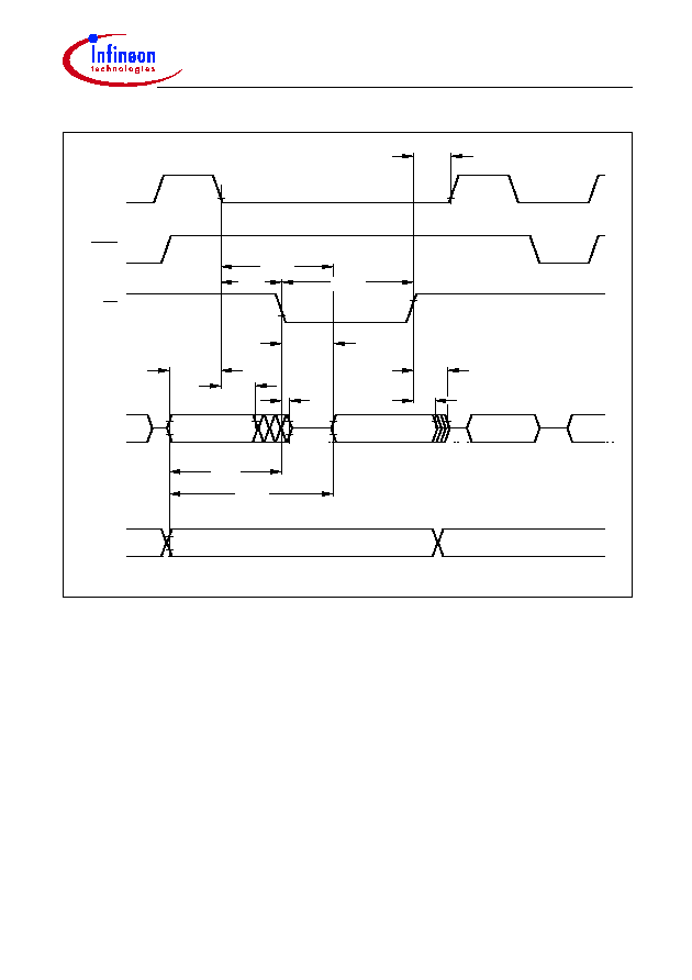
C513AO
Data Sheet
45
02.00
Figure 21
Data Memory Read Cycle
MCT00097
ALE
PSEN
Port 2
WHLH
t
Port 0
RD
t
LLDV
t
RLRH
t
LLWL
t
RLDV
t
AVLL
t
LLAX2
t
RLAZ
t
AVWL
t
AVDV
t
RHDX
t
RHDZ
A0 - A7 from
Ri or DPL
from PCL
A0 - A7
Instr.
IN
Data IN
A8 - A15 from PCH
P2.0 - P2.7 or A8 - A15 from DPH
c513ao_ds_0200.frm Page 45 Wednesday, August 30, 2000 12:45 PM

C513AO
Data Sheet
46
02.00
Figure 22
Data Memory Write Cycle
MCT00098
ALE
PSEN
Port 2
WHLH
t
Port 0
WR
t
WLWH
t
LLWL
t
QVWX
t
AVLL
t
LLAX2
t
QVWH
t
AVWL
t
WHQX
A0 - A7 from
Ri or DPL
from PCL
A0 - A7
Instr.IN
Data OUT
A8 - A15 from PCH
P2.0 - P2.7 or A8 - A15 from DPH
c513ao_ds_0200.frm Page 46 Wednesday, August 30, 2000 12:45 PM

C513AO
Data Sheet
47
02.00
Figure 23
SSC Timing
Figure 24
External Clock Drive on XTAL1
MCT02417
SCLK
STO
SRI
TC
t
SCL
MSB
LSB
MSB
LSB
SCH
t
t
SCLK
S
t
HI
t
~ ~
~~
~~
~~
~~
~ ~
D
t
t
HD
DTC
t
Notes: Shown is the data/clock relationship for CPOL = CPHA = 1. The timing diagram is
valid for the other cases accordingly.
In the case of slave mode and CPHA = 0, the output delay for the MSB applies to the
falling edge of SLS (if transmitter is enabled).
In the case of master mode and CPHA = 0, the MSB becomes valid after the data has
been written into the shift register, i.e. at least one half SCLK clock cycle before the
first clock transition.
MCT00033
t
CHCX
t
CLCX
CHCL
t
CLCH
t
V
DD
t
CLCL
- 0.5V
0.45V
DD
0.7
V
V - 0.1
DD
0.2
c513ao_ds_0200.frm Page 47 Wednesday, August 30, 2000 12:45 PM

C513AO
Data Sheet
48
02.00
OTP Memory Characteristics (C513AO-2E only)
Programming Mode Timing Characteristics
(Operating Conditions apply)
Parameter
Symbol
Limit Values
Unit
min.
max.
PALE Pulse Width
t
PAW
35
�
ns
PMSEL Set-up to PALE Rising Edge
t
PMS
10
�
�
Address Set-up to PALE, PROG, or PRD
Falling Edge
t
PAS
10
�
ns
Address Hold after PALE, PROG, or PRD
Falling Edge
t
PAH
10
�
ns
Address, Data Set-up to PROG or PRD
t
PCS
100
�
ns
Address, Data Hold after PROG or PRD
t
PCH
0
�
ns
PMSEL Set-up to PROG or PRD
t
PMS
10
�
ns
PMSEL Hold after PROG or PRD
t
PMH
10
�
ns
PROG Pulse Width
t
PWW
100
�
�
s
PRD Pulse Width
t
PRW
100
�
ns
Address to Valid Data out
t
PAD
�
75
ns
PRD to Valid Data out
t
PRD
�
20
ns
Data Hold after PRD
t
PDH
0
�
ns
Data float after PRD
t
PDF
�
20
ns
PROG High between two Consecutive
PROG Low Pulses
t
PWH1
1
�
�
s
PRD High between two Consecutive PRD
Low Pulses
t
PWH2
100
�
ns
XTAL Clock Period
t
CLKP
62.5
286
ns
c513ao_ds_0200.frm Page 48 Wednesday, August 30, 2000 12:45 PM

C513AO
Data Sheet
49
02.00
Figure 25
Programming Code Byte - Write Cycle Timing
A8-13
MCT04318
PALE
PMSEL1, 0
Port 2
Port 0
PROG
t
PMS
t
PAW
t
PAS
t
PAH
H, H
A0-7
D0-7
t
PWH
t
PWW
t
PCS
Notes: PRD must be high during a programming write cycle
t
PCH
c513ao_ds_0200.frm Page 49 Wednesday, August 30, 2000 12:45 PM

C513AO
Data Sheet
50
02.00
Figure 26
Verify Code Byte - Read Cycle Timing
A8-13
MCT04319
PALE
PMSEL1, 0
Port 2
Port 0
PRD
t
PMS
t
PAW
t
PAS
t
PAH
H, H
A0-7
t
PAD
D0-7
t
PDH
t
PRD
t
PWH
t
PRW
t
PCH
t
PCS
Notes: PROG must be high during a programming read cycle
t
PDF
c513ao_ds_0200.frm Page 50 Wednesday, August 30, 2000 12:45 PM

C513AO
Data Sheet
51
02.00
Figure 27
Lock Bit Access Timing
Figure 28
Version Registers - Read Timing
t
PDR
MCT04320
t
PCS
t
PMS
D0, D1
t
PCH
t
PMH
t
PWW
t
PRW
t
PMS
t
PRD
t
PMH
t
PDH
H, L
H, L
D0, D1
PMSEL1, 0
Port 0
PROG
PRD
Notes: PALE should be low during a lock bit read/write cycle
MCT04321
t
PRW
t
PCS
t
PDH
e.g. FD
H
D0-7
Port 2
Port 0
PRD
PMSEL1, 0
L, H
t
PCH
t
PMH
t
PDF
t
PRD
t
PMS
Notes: PROG must be high during a programming read cycle
c513ao_ds_0200.frm Page 51 Wednesday, August 30, 2000 12:45 PM

C513AO
Data Sheet
52
02.00
OTP Verification Mode Characteristics
Note: ALE pin described below is not the OTP Programming Mode pin PALE
Figure 29
OTP Verification Mode
Parameter
Symbol
Limit Values
Unit
min.
typ
max.
ALE Pulse Width
t
AWD
�
2
t
CLCL
�
ns
ALE Period
t
ACY
�
12
t
CLCL
�
ns
Data Valid after ALE
t
DVA
�
�
4
t
CLCL
ns
Data Stable after ALE
t
DSA
8
t
CLCL
�
�
ns
P3.5 Set-up to ALE Low
t
AS
�
t
CLCL
�
ns
Oscillator Frequency
1/
t
CLCL
4
�
6
MHz
MCT04322
ALE
Port 0
P3.5
t
ACY
t
AWD
t
DSA
t
DVA
t
AS
Data Valid
c513ao_ds_0200.frm Page 52 Wednesday, August 30, 2000 12:45 PM

C513AO
Data Sheet
53
02.00
Figure 30
AC Testing: Input, Output Waveforms
Figure 31
AC Testing: Float Waveforms
AC Inputs during testing are driven at
V
DD
� 0.5 V for a logic "1" and 0.45 V for a logic "0".
Timing measurements are made at
V
IHmin
for a logic "1" and
V
ILmax
for a logic "0".
0.45 V
V
DD
0.2
-0.1
+0.9
0.2
DD
V
Test Points
MCT00039
V
DD
-0.5 V
For timing purposes, a port pin is no longer floating when a 100 mV change from load voltage
occurs and begins to float when a 100 mV change from the loaded
V
OH
/
V
OL
level occurs.
I
OL
/
I
OH
�
20 mA.
MCT00038
V
Load
V
Load
-0.1 V
+0.1 V
Load
V
Timing Reference
Points
V
OH
-0.1 V
+0.1 V
OL
V
c513ao_ds_0200.frm Page 53 Wednesday, August 30, 2000 12:45 PM

C513AO
Data Sheet
54
02.00
Figure 32
Recommended Oscillator Circuits for Crystal Oscillator
MCS04317
3.5-16 MHz
C
C
Crystal Mode:
C
= 20 pF � 10 pF (incl. stray capacitance)
Crystal Oscillator Mode
External Oscillator
Signal
Driving from External Source
XTAL2
XTAL1
N.C.
XTAL2
XTAL1
c513ao_ds_0200.frm Page 54 Wednesday, August 30, 2000 12:45 PM

C513AO
Data Sheet
55
02.00
Package Outlines
G
P
D
0
5
0
5
5
2.54
1.5 max
0.45
+0.1
1.3
3.7
�0.3
0.5 min
5.1 max
40
21
1
20
50.9
-0.5
0.25 max
0.25
+0.1
14
-0.3
15.24
+1.2
15.24
�0.2
Index Marking
~
~
0.25 40x
Plastic Package, P-DIP-40-2
(Plastic Dual In-Line Package)
Sorts of Packing
Package outlines for tubes, trays etc. are contained in our
Data Book "Package Information".
Dimensions in mm
SMD = Surface Mounted Device
c513ao_ds_0200.frm Page 55 Wednesday, August 30, 2000 12:45 PM
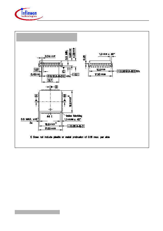
C513AO
Data Sheet
56
02.00
G
P
L
0
5
1
0
2
Plastic Package, P-LCC-44-1
(Plastic Lead Chip Carrier)
Sorts of Packing
Package outlines for tubes, trays etc. are contained in our
Data Book "Package Information".
Dimensions in mm
SMD = Surface Mounted Device
c513ao_ds_0200.frm Page 56 Wednesday, August 30, 2000 12:45 PM
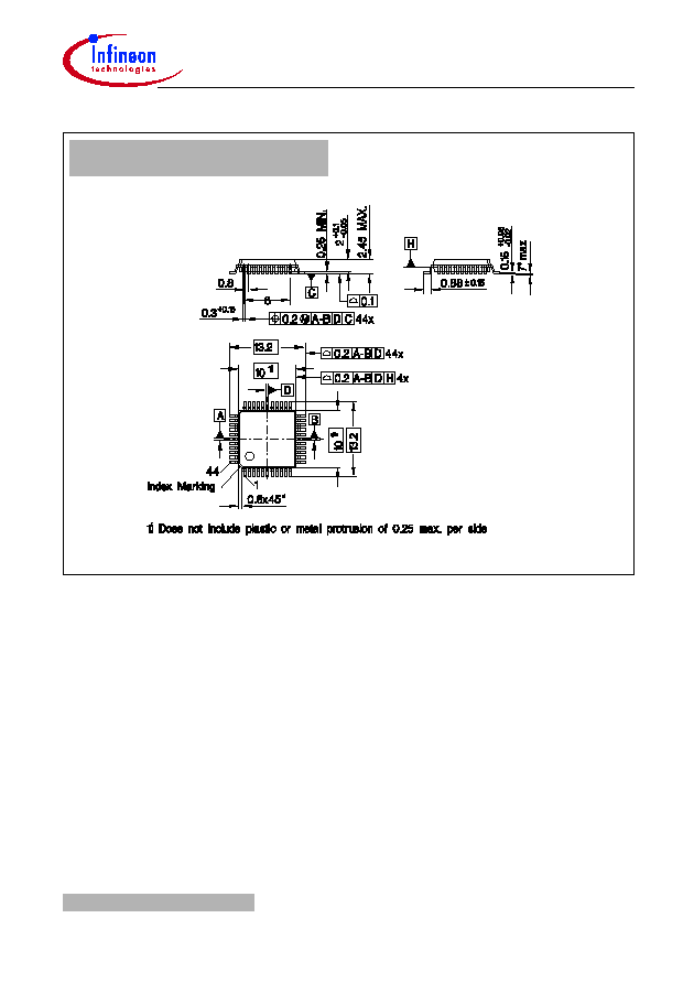
C513AO
Data Sheet
57
02.00
G
P
M
0
5
6
2
2
Plastic Package, P-MQFP-44-2
(Plastic Metric Quad Flat Pack)
Sorts of Packing
Package outlines for tubes, trays etc. are contained in our
Data Book "Package Information".
Dimensions in mm
SMD = Surface Mounted Device
c513ao_ds_0200.frm Page 57 Wednesday, August 30, 2000 12:45 PM