 | –≠–ª–µ–∫—Ç—Ä–æ–Ω–Ω—ã–π –∫–æ–º–ø–æ–Ω–µ–Ω—Ç: CFY66-10P | –°–∫–∞—á–∞—Ç—å:  PDF PDF  ZIP ZIP |
CFY66
Semiconductor Group
1 of 8
Draft D, September 99
HiRel K-Band GaAs Super Low Noise HEMT
∑
HiRel Discrete and Microwave Semiconductor
∑
Conventional AlGaAs/GaAs HEMT
(For new design we recommend to use our
pseudo-morphic HEMT CFY67)
∑
For professional super low-noise amplifiers
∑
For frequencies from 500 MHz to > 20 GHz
∑
Hermetically sealed microwave package
∑
Super low noise figure, high associated gain
∑
Space Qualified
ESA/SCC Detail Spec. No.: 5613/002,
Type Variant No.s 01 to 04
1
2
3
4
ESD: Electrostatic discharge sensitive device, observe handling precautions!
Type
Marking
Ordering Code Pin Configuration
Package
1
2
3
4
CFY66-08 (ql)
CFY66-08P (ql)
CFY66-10 (ql)
CFY66-10P (ql)
-
see below
G
S
D
S
Micro-X
CFY66-nnl: specifies gain and output power levels (see electrical characteristics)
(ql) Quality Level:
P: Professional Quality,
Ordering Code:
on request
H: High Rel Quality,
Ordering Code:
on request
S: Space Quality,
Ordering Code:
on request
ES: ESA Space Quality,
Ordering Code:
on request
(see order instructions for ordering example)

CFY66
Semiconductor Group
2 of 8
Draft D, September 99
Maximum Ratings
Parameter
Symbol
Values
Unit
Drain-source voltage
V
DS
3.5
V
Drain-gate voltage
V
DG
4.5
V
Gate-source voltage (reverse / forward)
V
GS
- 3... + 0.5
V
Drain current
I
D
60
mA
Gate forward current
I
G
2
mA
RF Input Power, C- and X-Band
1)
P
RF,in
+ 10
dBm
Junction temperature
T
J
150
∞
C
Storage temperature range
T
stg
- 65... + 150
∞
C
Total power dissipation
2)
P
tot
200
mW
Soldering temperature
3)
T
sol
230
∞C
Thermal Resistance
Junction-soldering point
R
th JS
515 (tbc.)
K/W
Notes.:
1) For V
DS
2 V. For V
DS
> 2 V, derating is required.
2) At T
S
= + 47 ∞C. For T
S
> + 47 ∞C derating is required.
3) During 15 sec. maximum. The same terminal shall not be resoldered until 3 minutes have
elapsed.
CFY66
Semiconductor Group
3 of 8
Draft D, September 99
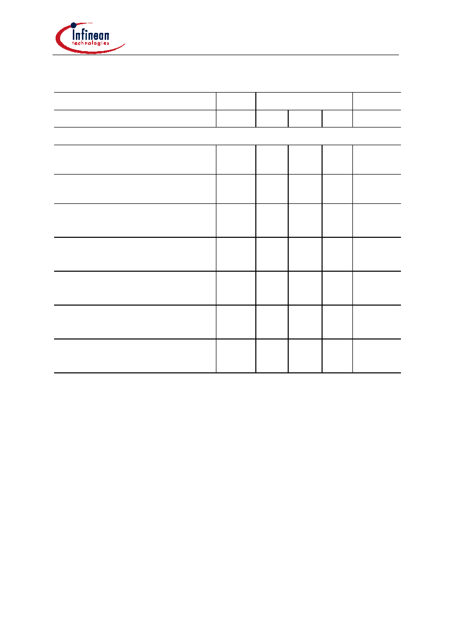
Electrical Characteristics
(at T
A
=25∞C; unless otherwise specified)
Parameter
Symbol
Values
Unit
min.
typ.
max.
DC Characteristics
Drain-source saturation current
V
DS
= 2 V, V
GS
= 0 V
I
Dss
10
30
60
mA
Gate threshold voltage
V
DS
= 2 V, I
D
= 1 mA
-V
Gth
0.2
0.7
2.0
V
Drain current at pinch-off
V
DS
= 1.5 V, V
GS
= - 3 V
I
Dp
-
< 50
-
µA
Gate leakage current at pinch-off
V
DS
= 1.5 V, V
GS
= - 3 V
-I
Gp
-
< 50
200
µA
Transconductance
V
DS
= 2 V, I
D
= 10 mA
g
m10
40
55
-
mS
Gate leakage current at operation
V
DS
= 2 V, I
D
= 10 mA
-I
G10
-
< 0.5
2
µA
Thermal resistance
junction to soldering point
R
th JS
-
450
-
K/W
CFY66
Semiconductor Group
4 of 8
Draft D, September 99
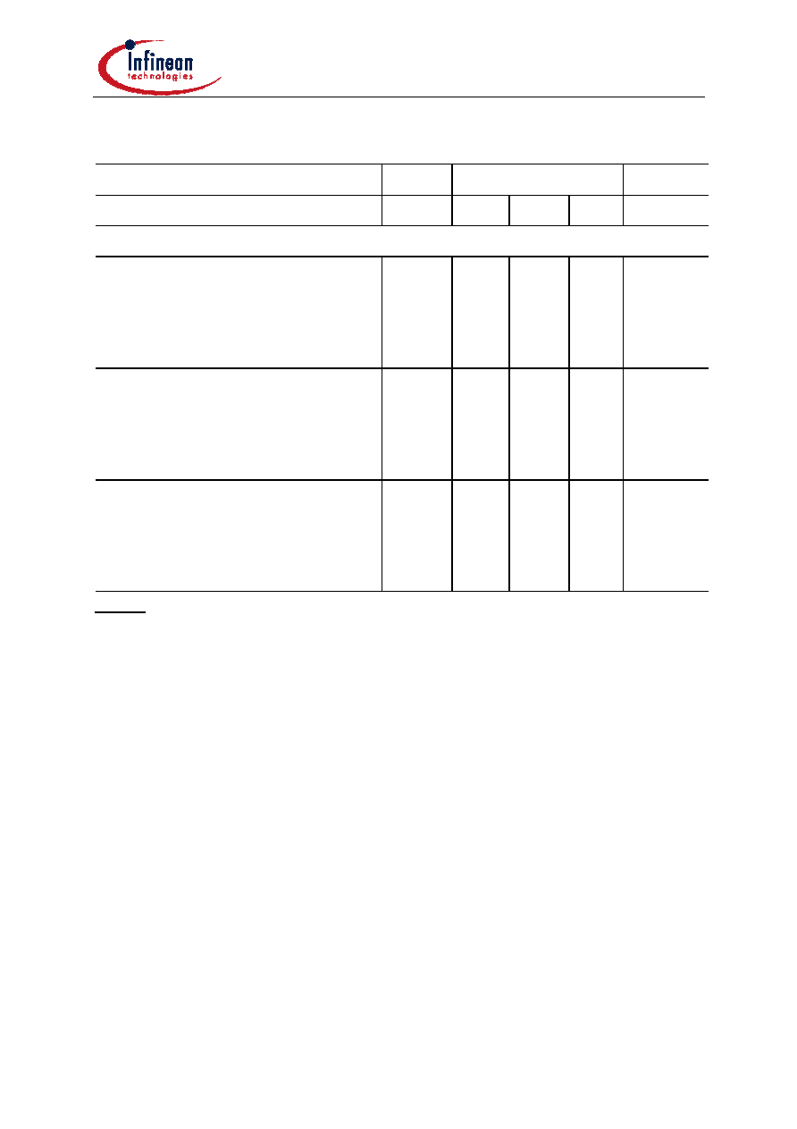
Electrical Characteristics
(continued)
Parameter
Symbol
Values
Unit
min.
typ.
max.
AC Characteristics
Noise figure
1)
V
DS
= 2 V, I
D
= 10 mA, f = 12 GHz
NF
dB
CFY66-08, -08P
-
0.7
0.8
CFY66-10, 10P
-
0.9
1.0
Associated gain.
1)
V
DS
= 2 V, I
D
= 10 mA, f = 12 GHz
G
a
dB
CFY66-08, -08P
10.0
11.0
-
CFY66-10, 10P
9.5
10.5
-
Output power at 1 dB gain compression
2)
V
DS
= 2 V, I
D
= 20 mA, f = 12 GHz
P
1dB
dBm
CFY66-06, -08, -10
-
11.0
-
CFY66-08P, -10P
10.0
11.0
-
Notes.:
1) Noise figure / sssociated gain characteristics given for minimum noise figure matching
conditions (fixed generic matching, no fine-tuning).
2) Output power characteristics given for optimum output power matching conditions (fixed
generic matching, no fine-tuning).
CFY66
Semiconductor Group
5 of 8
Draft D, September 99
Typical Common Source S-Parameters
CFY66-08: V
DS
= 2 V, I
D
= 10 mA, Z
o
= 50
f
|S11|
<S11
|S21|
<S21
|S12|
<S12
|S22|
<S22 k-Fact. S
21
/S
12
MAG
[GHz] [magn] [angle] [magn] [angle] [magn] [angle] [magn] [angle] [magn]
[dB]
[dB]
1,0
0,990
-21
4,451
161
0,0260
70
0,649
-16
0,14
22,3
2,0
0,960
-39
4,282
144
0,0460
61
0,623
-29
0,19
19,7
3,0
0,920
-57
4,148
126
0,0650
49
0,589
-43
0,27
18,0
4,0
0,880
-77
3,979
108
0,0830
37
0,560
-57
0,32
16,8
5,0
0,830
-95
3,727
93
0,0940
25
0,532
-70
0,39
16,0
6,0
0,790
-111
3,444
78
0,1000
14
0,506
-83
0,47
15,4
7,0
0,749
-124
3,206
64
0,1060
6
0,490
-94
0,55
14,8
8,0
0,720
-137
3,029
50
0,1110
-3
0,463
-103
0,63
14,4
9,0
0,690
-150
2,907
38
0,1130
-11
0,440
-113
0,70
14,1
10,0
0,670
-165
2,845
25
0,1190
-20
0,420
-121
0,74
13,8
11,0
0,649
179
2,787
11
0,1210
-28
0,400
-130
0,79
13,6
12,0
0,628
164
2,699
-3
0,1200
-37
0,385
-143
0,84
13,5
13,0
0,610
151
2,614
-16
0,1200
-46
0,370
-153
0,91
13,4
14,0
0,597
138
2,584
-28
0,1190
-55
0,355
-162
0,96
13,4
15,0
0,584
121
2,550
-42
0,1180
-66
0,340
-172
1,01
13,3
12,8
16,0
0,580
104
2,484
-56
0,1170
-76
0,330
178
1,05
13,3
11,9
17,0
0,580
89
2,461
-71
0,1150
-87
0,325
169
1,08
13,3
11,5
18,0
0,580
74
2,456
-86
0,1160 -100
0,320
160
1,09
13,3
11,4
Typical Common Source Noise-Parameters
CFY66-08: V
DS
= 2 V, I
D
= 10 mA, Z
o
= 50
f
NF
min
|
opt
|
<
opt
R
n
[GHz]
[dB]
[magn]
[angle]
[
]
1
0,27
0,770
16
17,85
2
0,31
0,720
30
16,55
3
0,35
0,672
43
15,27
4
0,38
0,634
57
13,75
5
0,42
0,604
71
11,99
6
0,46
0,578
85
10,04
7
0,50
0,558
100
8,15
8
0,55
0,541
114
6,30
9
0,60
0,528
128
4,74
10
0,65
0,517
143
3,45
11
0,70
0,506
157
2,58
12
0,74
0,496
171
2,16
13
0,79
0,485
-175
2,27
14
0,85
0,472
-160
2,88
15
0,89
0,457
-146
3,99
16
0,95
0,437
-132
5,59
17
1,00
0,415
-118
7,63
18
1,06
0,389
-102
9,96

CFY66
Semiconductor Group
6 of 8
Draft D, September 99
Order Instructions:
Full type variant including quality level must be specified by the orderer. For HiRel Discrete
and Microwave Semiconductors the ordering code specifies device family and quality level
only.
Ordering Form:
Ordering Code: Q..........
CFY66 -(nnl) (ql)
-(nnl)
Noise Figure/Gain and/or Power Level
(ql):
Quality Level
Ordering Example:
Ordering Code: (on request)
CFY66-08P ES
For CFY66, Noise Figure/Gain/Power Level 08P:
NF < 0.8 dB, G
a
> 10.0 dB, P
1dB
> 10 dBm @ 12 GHz
in ESA Space Quality Level
Further Informations:
See our WWW-Pages:
- Discrete and RF-Semiconductors (Small Signal Semiconductors)
www.infineon.com/products/discrete/hirel.htm
- HiRel Discrete and Microwave Semiconductors
www.infineon.com/products/discrete/hirel.htm
Please contact also our marketing division :
Tel.:
++89 234 24480
Fax.:
++89 234 28434
e-mail: martin.wimmers@infineon.com
Address:
Infineon Technologies Semiconductors,
High Frequency Products Marketing,
P.O.Box 801709,
D-81617 Munich

CFY66
Semiconductor Group
7 of 8
Draft D, September 99
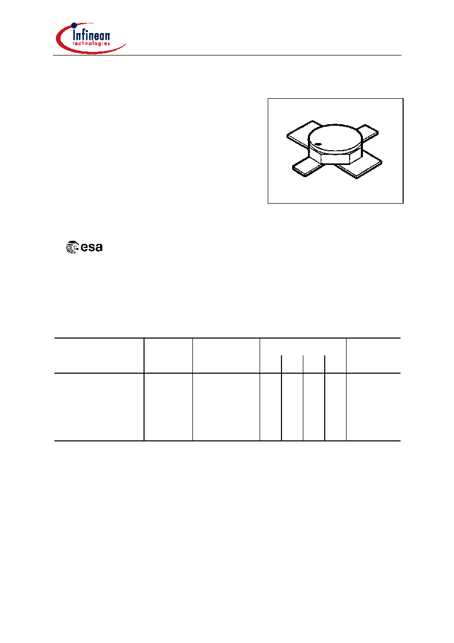
Micro-X Package
Published by Infineon Technologies Semiconductors,
High Frequency Products Marketing, P.O.Box 801709,
D-81617 Munich.
Infineon Technologies AG 1998. All Rights Reserved.
As far as patents or other rights of third parties are
concerned, liability is only assumed for components per
se, not for applications, processes and circuits
implemented within components or assemblies.
The information describes the type of component and shall
not be considered as assured characteristics.
Terms of delivery and rights to change design reserved.
For questions on technology, delivery and prices please
contact the Offices of Semiconductor Group in Germany or
the Infineon Technologies Companies and
Representatives woldwide (see address list).
Due to technical requirements components may contain
dangerous substances. For information on the type in
question please contact your nearest Infineon
Technologies Office, Semiconductor Group.
Infineon Technologies Semiconductors is a certified CECC
and QS9000 manufacturer (this includes ISO 9000).