FOA4400/9400/5400/5401
P
R
O
D
U
C
T
B
R
I
E
F
N e v e r s t o p t h i n k i n g .
Features
s
Supports data rates from
39.8 Gbit/s to 43 Gbit/s
s
Infineon's leading-edge SiGe
B7HF technology
s
1:16 (= 1:2 and 2:16) and 16:1
multiplexing ratio
s
On-chip VCO, external VCO
input available
s
622 MHz or 2.5 GHz reference
clock
s
Adjustable sampling
threshold and phase
s
Integrated pre-amplifier with
high input sensitivity
s
Selectable 20 GHz and
40 GHz output clock
s
FIFO depth of 6 Bits
Typical Applications
s
Fiber optics telecom and
datacom applications
s
SONET/SDH OC-768/STM-256
with and without FEC
Main Advantages
s
Data rate from 39.8 Gbit/s
up to 43 Gbit/s
s
SiGe chipset providing
complete functionality:
CMU, CDR, FIFO and VCO
s
Single supply voltage of 5.5 V
s
High CDR sensitivity with
adjustable sampling
s
On-chip VCO together with
external VCO input
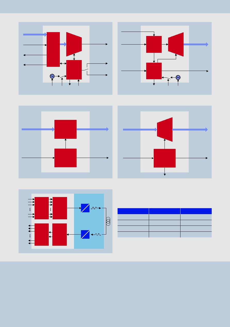
MUX Evaluation Board
F O A 4 4 0 0 / 9 4 0 0 /
5 4 0 0 / 5 4 0 1
M U X / F I F O / D E M U X / C D R
3 9 . 8 - 4 3 G b i t / s , 5 . 5 V
S e m i c o n d u c t o r S o l u t i o n s f o r
H i g h S p e e d C o m m u n i c a t i o n
a n d F i b e r O p t i c A p p l i c a t i o n s
FOA4400 16:1 MUX
Multiplexer with Clock Multiplication Unit
MUX 39.8 - 43 Gbit/s, 5.5 V
FOA9400 1:1 FIFO
Data Synchronization
FIFO 2.5 - 2.7 Gbit/s, 5.5 V
FOA5400 2:16 DEMUX
Demultiplexer
DEMUX 39.8 - 43 Gbit/s, 5.5 V
FOA5401 1:2 CDR
Clock and Data Recovery with 1:2 Demultiplexer
CDR 39.8 - 43 Gbit/s, 5.5 V
The 40 Gbit/s transceiver chipset (MUX+FIFO and CDR+DEMUX)
provide highly integrated SerDes (SERializer-DESerializer) func-
tionality with a 1:16 ratio. The 16 times 2.5 Gbit/s data signals
are multiplexed to a single serial 40 Gbit/s data stream and vice
versa. The devices support datarates from 39.8 Gbit/s up to
43 Gbit/s (OC-768/STM-256) with optional FEC (Forward Error
Correction). All four chips are manufactured in Infineon's
leading-edge Silicon-Germanium B7HF technology enabling low
power consumption.
The multiplexer FOA4400, FIFO FOA9400, demultiplexer FOA5400
and CDR FOA5401 feature CML interfaces, integrated VCOs
(Voltage-Controlled Oscillator) and two reference clocks
(622 MHz/2.5 GHz). The FOA4400 incorporates the CMU and
selectable 20 GHz and 40 GHz clock outputs, whereas optional
data synchronization is provided by the FOA9400. The FOA5400
and FOA5401 integrate CDR and demultiplexing functionality
with extremely high input sensitivity.
CDR-DEMUX Evaluation Board
P
R
O
D
U
C
T
B
R
I
E
F
Published by Infineon Technologies AG
How to reach us:
http://www.infineon.com
Published by
Infineon Technologies AG,
St.-Martin-Strasse 53,
81541 M�nchen
� Infineon Technologies AG 2002. All Rights Reserved.
Attention please!
The information herein is given to describe certain components
and shall not be considered as warranted characteristics.
Terms of delivery and rights to technical change reserved.
We hereby disclaim any and all warranties, including but not
limited to warranties of non-infringement, regarding circuits,
descriptions and charts stated herein.
Infineon Technologies is an approved CECC manufacturer.
Information
For further information on technology, delivery terms
and conditions and prices please contact your nearest
Infineon Technologies Office in Germany or our
Infineon Technologies Representatives worldwide.
Warnings
Due to technical requirements components may contain danger-
ous substances. For information on the types in question please
contact your nearest Infineon Technologies Office.
Infineon Technologies Components may only be used in life-
support devices or systems with the express written approval
of Infineon Technologies, if a failure of such components can
reasonably be expected to cause the failure of that life-support
device or system, or to affect the safety or effectiveness of that
device or system. Life support devices or systems are intended
to be implanted in the human body, or to support and/or main-
tain and sustain and/or protect human life. If they fail, it is rea-
sonable to assume that the health of the user or other persons
may be endangered.
FOA4400 MUX Block Diagram
Register
16:1
MUX
CMU
&
PD
VCO
Data IN
16 x 2.5 Gbit/s
Data OUT
39.8-43 Gbit/s
Clock IN
2.5 GHz
Clock OUT
2.5 GHz
Clock OUT
622 MHz
Clock OUT
20 GHz
Clock OUT
40 GHz
VCO
CTRL
Extern
VCO
PD
OUT
Reference Clock
622 MHz / 2.5 GHz
M U X F OA 4 4 0 0
FOA9400
1:1
FIFO
(optional)
16
x
2.
5 Gbit/s
Input
Dat
a Ch
annels
40 Gbit/s
40 Gbit/s
16
x
2.
5 Gbit/s
Output
Dat
a Ch
annels
FOA5400
2:16
DEMUX
FOA5401
CDR &
1:2
DEMUX
FOA4400
16:1
MUX
E
O
E
O
40 Gbit/s Chipset Overview
Ordering No. B168-H7899-G1-X-7600
Printed in Germany
PS 1201.5
NB
PREAMP
VCO
Data OUT
2 x 20 Gbit/s
Data IN
39.8-43 Gbit/s
VCO
CTRL
Extern
VCO
PD
OUT
CDR FOA5401
1:2
DEMUX
CDR
Phase Adjust
Clock OUT
20 GHz
Threshold
Adjust
FOA5400 DEMUX Block Diagram
FOA5401 CDR Block Diagram
Data OUT
16 x 2.5 Gbit/s
Data IN
2 x 20 Gbit/s
DEMUX FOA5400
2:16
DEMUX
CLK
Management
CLK IN
20 GHz
CLK OUT
2.5 GHz
CLK OUT
1.25 GHz
19 MHz
FOA9400 FIFO Block Diagram
Data OUT
16 x 2.5 Gbit/s
Data IN
16 x 2.5 Gbit/s
FIFO FOA9400
CLK
Management
16:16 FIFO
CLK IN
1.25 GHz
CLK OUT
2.5 GHz
CLK OUT
1.25 GHz
Packing
Type
Sales Code
Package
MUX 16:1
FOA4400
Bare Die
FIFO 1:1
FOA9400
Bare Die
DEMUX 2:16
FOA5400
Bare Die
CDR 1:2
FOA5401
Bare Die