
CoolSETTM-F3
(Jitter Version)
ICE3B0365J
ICE3B0565J
ICE3B1565J
Off-Line SMPS Current Mode
Controller with integrated 650V
Startup Cell/Depletion CoolMOSTM
N e v e r s t o p t h i n k i n g .
Power Management & Supply
Version 2.3, 8 May 2006

Edition 2006-05-08
Published by
Infineon Technologies AG
81726 M¸nchen, Germany
©
Infineon Technologies AG 5/8/06.
All Rights Reserved.
Attention please!
The information given in this data sheet shall in no event be regarded as a guarantee of conditions or
characteristics ("Beschaffenheitsgarantie"). With respect to any examples or hints given herein, any typical values
stated herein and/or any information regarding the application of the device, Infineon Technologies hereby
disclaims any and all warranties and liabilities of any kind, including without limitation warranties of
non-infringement of intellectual property rights of any third party.
Information
For further information on technology, delivery terms and conditions and prices please contact your nearest
Infineon Technologies Office (
www.infineon.com
).
Warnings
Due to technical requirements components may contain dangerous substances. For information on the types in
question please contact your nearest Infineon Technologies Office.
Infineon Technologies Components may only be used in life-support devices or systems with the express written
approval of Infineon Technologies, if a failure of such components can reasonably be expected to cause the failure
of that life-support device or system, or to affect the safety or effectiveness of that device or system. Life support
devices or systems are intended to be implanted in the human body, or to support and/or maintain and sustain
and/or protect human life. If they fail, it is reasonable to assume that the health of the user or other persons may
be endangered.
For questions on technology, delivery and prices please contact the Infineon Technologies Offices in Germany or
the Infineon Technologies Companies and Representatives worldwide: see our webpage at http://
www.infineon.com
CoolMOSTM, CoolSETTM are trademarks of Infineon Technologies AG.
CoolSETTM-F3
ICE3Bxx65J
Revision History:
2006-05-08
Datasheet
Previous Version: 2.2 ( ICE3B0365J/ICE3B0565J ), 2.0 ( ICE3B1565J )
Page
Subjects (major changes since last revision)
Group ICE3B0365J, ICE3B0565J and ICE3B1565J together
6, 8, 12, 13
revise typo to the trigger level in Vsofts ( C2 ) and VFB ( C6a )
11, 12
revise typo in figure 13 and 14
Type
Package
Marking
V
DS
F
OSC
R
DSon
1)
1)
typ @ T=25∞C
230VAC ±15%
2)
85-265 VAC
2)
ICE3B0365J
PG-DIP-8-6
ICE3B0365J
650V
67kHz
6.45
22W
10W
ICE3B0565J
PG-DIP-8-6
ICE3B0565J
650V
67kHz
4.70
25W
12W
ICE3B1565J
PG-DIP-8-6
ICE3B1565J
650V
67kHz
1.70
42W
20W
2)
Calculated maximum input power rating at Ta=75∞C, Tj=125∞C and without copper area as heat sink
Version 2.3
3
8 May 2006
CoolSETTM-F3
ICE3Bxx65J
Off-Line SMPS Current Mode Controller with
integrated 650V Startup Cell/Depletion CoolMOSTM
test
PG-DIP-8-6
Product Highlights
∑ Active Burst Mode to reach the lowest
Standby Power Requirements < 100mW
∑ Adjustable Blanking Window for High Load
Jumps to increase Reliability
∑ Frequency Jittering for Low EMI
∑ Pb-free lead plating, RoHS compilant
Features
∑ 650V Avalanche Rugged CoolMOSTM with built in
switchable Startup Cell
∑ Active Burst Mode for lowest Standby Power
@ light load controlled by Feedback Signal
∑ Fast Load Jump Response in Active Burst Mode
∑ 67 kHz fixed Switching Frequency
∑ Auto Restart Mode for Over temperature
Detection
∑ Auto Restart Mode for Overvoltage Detection
∑ Auto Restart Mode for Overload and Open Loop
∑ Auto Restart Mode for VCC Undervoltage
∑ User defined Soft Start
∑ Minimum of external Components required
∑ Max Duty Cycle 75%
∑ Overall Tolerance of Current Limiting < ±5%
∑ Internal Leading Edge Blanking
∑ BiCMOS technology provides wide VCC Range
∑ Frequency Jittering for Low EMI
Description
The CoolSETTM-F3(Jitter version) meets the requirements
for Off-Line Battery Adapters and low cost SMPS for the
lower power range. By use of a BiCMOS technology a wide
VCC range up to 26V is provided. This covers the changes
in the auxiliary supply voltage if a CV/CC regulation is
implemented on the secondary side. Furthermore an Active
Burst Mode is integrated to fullfill the lowest Standby Power
Requirements <100mW at no load and V
in
= 270VAC. As
during Active Burst Mode the controller is always active
there is an immediate response on load jumps possible
without any black out in the SMPS. In Active Burst Mode
the ripple of the output voltage can be reduced <1%.
Furthermore Auto Restart Mode is entered in case of
Overtemperature, VCC Overvoltage, Output Open loop or
Overload and VCC Undervoltage. By means of the internal
precise peak current limitation, the dimension of the
transformer and the secondary diode can be lowered which
leads to more cost efficiency.
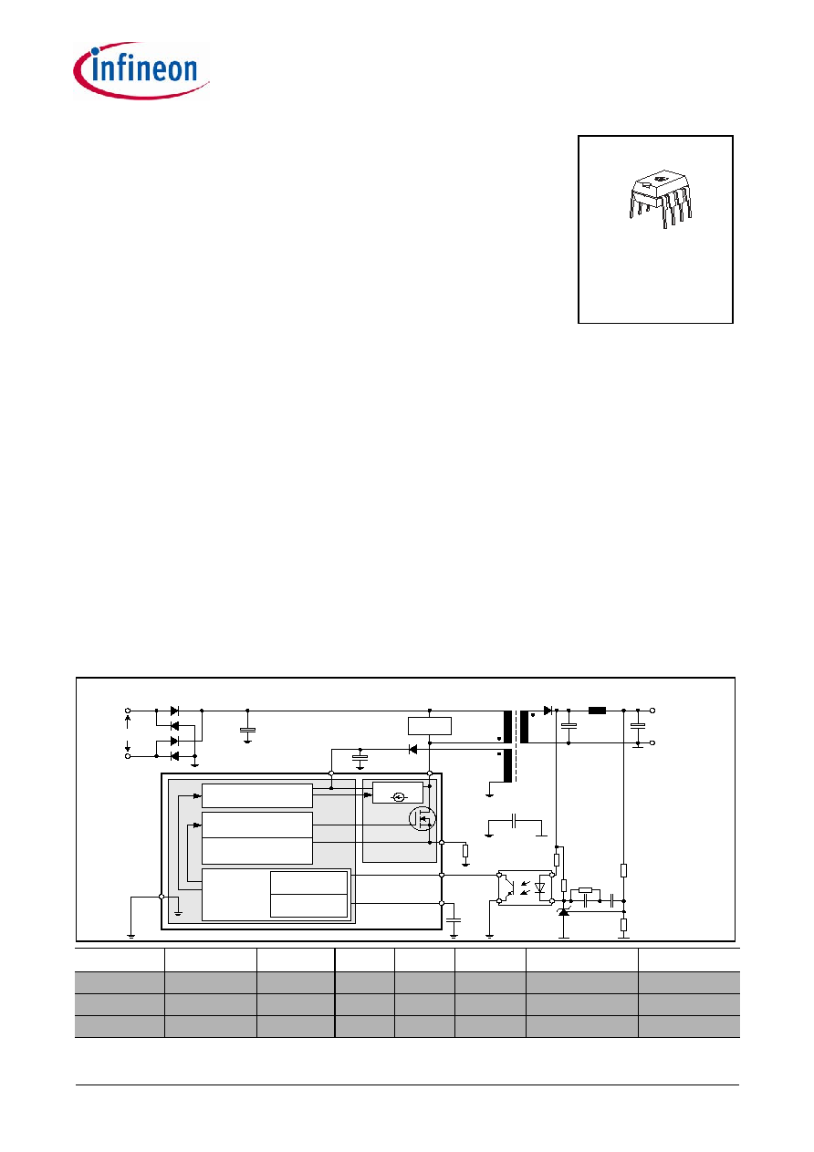
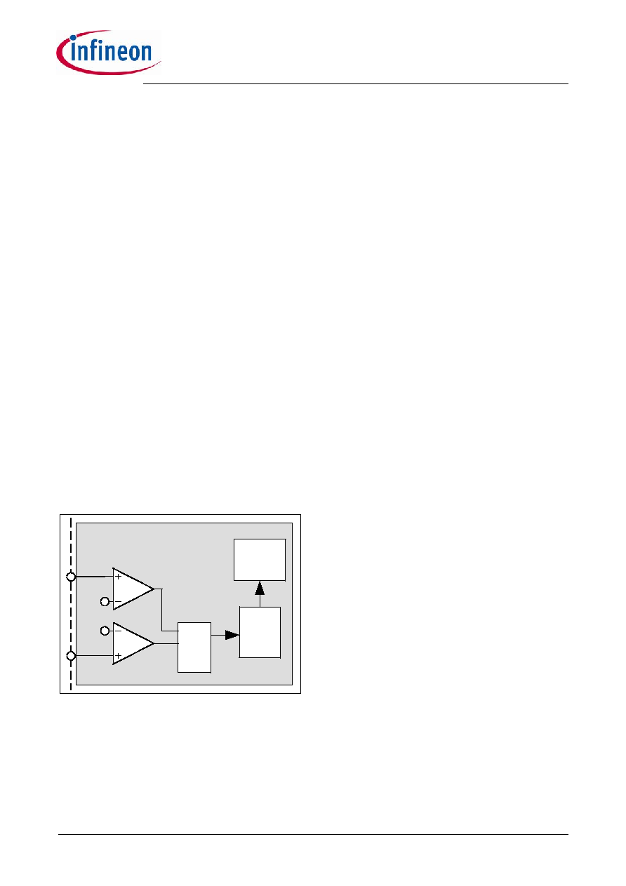
C
SoftS
C
VCC
C
Bulk
Converter
DC Output
+
Snubber
Power Management
PWM Controller
Current Mode
85 ... 270 VAC
Typical Application
R
Sense
SoftS
FB
GND
Active Burst Mode
Auto Restart Mode
Control
Unit
-
CS
VCC
Startup Cell
Precise Low Tolerance Peak
Current Limitation
Drain
CoolSETTM-F3
(Jitter Version)
Depl. CoolMOSTM

CoolSETTM-F3
ICE3Bxx65J
Table of Contents
Page
Version 2.3
4
8 May 2006
1
Pin Configuration and Functionality . . . . . . . . . . . . . . . . . . . . . . . . . . . . .5
1.1
Pin Configuration with PG-DIP-8-6 . . . . . . . . . . . . . . . . . . . . . . . . . . . . . . . .5
1.2
Pin Functionality . . . . . . . . . . . . . . . . . . . . . . . . . . . . . . . . . . . . . . . . . . . . . .5
2
Representative Blockdiagram . . . . . . . . . . . . . . . . . . . . . . . . . . . . . . . . . .6
3
Functional Description . . . . . . . . . . . . . . . . . . . . . . . . . . . . . . . . . . . . . . . .7
3.1
Introduction . . . . . . . . . . . . . . . . . . . . . . . . . . . . . . . . . . . . . . . . . . . . . . . . . .7
3.2
Power Management . . . . . . . . . . . . . . . . . . . . . . . . . . . . . . . . . . . . . . . . . . . .7
3.3
Startup Phase . . . . . . . . . . . . . . . . . . . . . . . . . . . . . . . . . . . . . . . . . . . . . . . .8
3.4
PWM Section . . . . . . . . . . . . . . . . . . . . . . . . . . . . . . . . . . . . . . . . . . . . . . . . .9
3.4.1
Oscillator . . . . . . . . . . . . . . . . . . . . . . . . . . . . . . . . . . . . . . . . . . . . . . . . . .9
3.4.2
PWM-Latch FF1 . . . . . . . . . . . . . . . . . . . . . . . . . . . . . . . . . . . . . . . . . . . . .9
3.4.3
Gate Driver . . . . . . . . . . . . . . . . . . . . . . . . . . . . . . . . . . . . . . . . . . . . . . . .9
3.5
Current Limiting . . . . . . . . . . . . . . . . . . . . . . . . . . . . . . . . . . . . . . . . . . . . . .10
3.5.1
Leading Edge Blanking . . . . . . . . . . . . . . . . . . . . . . . . . . . . . . . . . . . . . .10
3.5.2
Propagation Delay Compensation . . . . . . . . . . . . . . . . . . . . . . . . . . . . . .10
3.6
Control Unit . . . . . . . . . . . . . . . . . . . . . . . . . . . . . . . . . . . . . . . . . . . . . . . . .11
3.6.1
Adjustable Blanking Window . . . . . . . . . . . . . . . . . . . . . . . . . . . . . . . . . .11
3.6.2
Active Burst Mode . . . . . . . . . . . . . . . . . . . . . . . . . . . . . . . . . . . . . . . . . .12
3.6.2.1
Entering Active Burst Mode . . . . . . . . . . . . . . . . . . . . . . . . . . . . . . . . .12
3.6.2.2
Working in Active Burst Mode . . . . . . . . . . . . . . . . . . . . . . . . . . . . . . .12
3.6.2.3
Leaving Active Burst Mode . . . . . . . . . . . . . . . . . . . . . . . . . . . . . . . . .12
3.6.3
Protection Modes . . . . . . . . . . . . . . . . . . . . . . . . . . . . . . . . . . . . . . . . . . .13
3.6.3.1
Auto Restart Mode . . . . . . . . . . . . . . . . . . . . . . . . . . . . . . . . . . . . . . . .14
4
Electrical Characteristics . . . . . . . . . . . . . . . . . . . . . . . . . . . . . . . . . . . . .15
4.1
Absolute Maximum Ratings . . . . . . . . . . . . . . . . . . . . . . . . . . . . . . . . . . . . .15
4.2
Operating Range . . . . . . . . . . . . . . . . . . . . . . . . . . . . . . . . . . . . . . . . . . . . .16
4.3
Characteristics . . . . . . . . . . . . . . . . . . . . . . . . . . . . . . . . . . . . . . . . . . . . . . .16
4.3.1
Supply Section . . . . . . . . . . . . . . . . . . . . . . . . . . . . . . . . . . . . . . . . . . . . .16
4.3.2
Internal Voltage Reference . . . . . . . . . . . . . . . . . . . . . . . . . . . . . . . . . . .17
4.3.3
PWM Section . . . . . . . . . . . . . . . . . . . . . . . . . . . . . . . . . . . . . . . . . . . . . .17
4.3.4
Control Unit . . . . . . . . . . . . . . . . . . . . . . . . . . . . . . . . . . . . . . . . . . . . . . .17
4.3.5
Current Limiting . . . . . . . . . . . . . . . . . . . . . . . . . . . . . . . . . . . . . . . . . . . .18
4.3.6
CoolMOSTM Section . . . . . . . . . . . . . . . . . . . . . . . . . . . . . . . . . . . . . . . . .18
5
Temperature derating curve . . . . . . . . . . . . . . . . . . . . . . . . . . . . . . . . . . .19
6
Outline Dimension . . . . . . . . . . . . . . . . . . . . . . . . . . . . . . . . . . . . . . . . . . .21
7
Marking . . . . . . . . . . . . . . . . . . . . . . . . . . . . . . . . . . . . . . . . . . . . . . . . . . . .22
8
Schematic for recommended PCB layout . . . . . . . . . . . . . . . . . . . . . . . .24

Version 2.3
5
8 May 2006
CoolSETTM-F3
ICE3Bxx65J
1
Pin Configuration and Functionality
1.1
Pin Configuration with PG-DIP-8-6
Figure 1
Pin Configuration PG-DIP-8-6(top view)
Note:
Pin 4 and 5 are shorted within the DIP
package.
1.2
Pin Functionality
SoftS (Soft Start, Auto Restart & Frequency
Jittering Control)
The SoftS pin combines the function of Soft Start
during Start Up and error detection for Auto Restart
Mode. These functions are implemented and can be
adjusted by means of an external capacitor at SoftS to
ground. This capacitor also provides an adjustable
blanking window for high load jumps, before the IC
enters into Auto Restart Mode. Furthermore this pin is
also used to control the period of frequency jittering
during normal load.
FB (Feedback)
The information about the regulation is provided by the
FB Pin to the internal Protection Unit and to the internal
PWM-Comparator to control the duty cycle. The FB-
Signal controls in case of light load the Active Burst
Mode of the controller.
CS (Current Sense)
The Current Sense pin senses the voltage developed
on the series resistor inserted in the source of the
integrated Depl. CoolMOSTM. If CS reaches the internal
threshold of the Current Limit Comparator, the Driver
output is immediately switched off. Furthermore the
current information is provided for the PWM-
Comparator to realize the Current Mode.
Drain (Drain of integrated Depl. CoolMOSTM)
Pin Drain is the connection to the Drain of the internal
Depl. CoolMOS
TM
.
VCC (Power supply)
The VCC pin is the positive supply of the IC. The
operating range is between 10.3V and 26V.
GND (Ground)
The GND pin is the ground of the controller.
Pin
Symbol
Function
1
SoftS
Soft-Start
2
FB
Feedback
3
CS
Current Sense/
650V
1)
Depl. CoolMOSTM Source
4
Drain
650V
1)
Depl. CoolMOSTM Drain
1)
at T
j
= 110∞C
5
Drain
650V
1)
Depl. CoolMOSTM Drain
6
N.C.
Not Connected
7
VCC
Controller Supply Voltage
8
GND
Controller Ground
Package PG-DIP-8-6
1
6
7
8
4
3
2
5
GND
SoftS
FB
CS
VCC
N.C
Drain
Drain

Version 2.3
6
8 May 2006
CoolSETTM-F3
ICE3Bxx65J
I
n
t
e
r
nal
B
i
as
V
o
l
t
age
R
e
f
e
r
enc
e
O
s
c
illa
t
o
r
Du
t
y
Cy
c
l
e
ma
x
x3.
2
S
o
ft
-
S
ta
r
t
C
o
m
par
at
or
C
u
rr
e
n
t L
i
m
i
ti
n
g
PW
M
O
P
Cu
r
r
e
n
t
M
o
d
e
Sof
t
St
a
r
t
C2
3.
1V
R
FB
P
o
w
e
r
M
a
n
a
gem
e
nt
C
So
f
t
S
C
VC
C
85 .
.
.
270 V
A
C
C
Bu
l
k
+
C
onv
er
t
e
r
DC
O
u
t
p
u
t
V
OU
T
Sp
i
k
e
B
l
anki
n
g
8.
0
us
PW
M
C
o
m
par
at
or
C3
4.
0V
C4
4.
5V
R
S
o
ftS
Ga
t
e
Dr
i
v
e
r
0.
7
5
Cl
o
c
k
R
Se
n
s
e
0.
6V
10k
D1
T2
C6
a
3.
0V
C5
1.
35V
C1
0
R
S
Q
A
u
to
R
e
s
t
a
r
t
M
ode
&
G7
&
G5
&
G9
1
G8
Ther
m
a
l
S
hut
dow
n
T
j
>14
0
∞
C
3.
25k
3V
S1
5V
T1
P
o
w
e
r-D
o
w
n
Re
s
e
t
CS
So
f
t
S
GN
D
C7
C8
FB
PW
M
S
ect
i
o
n
C
o
n
t
r
o
l U
n
it
FF
1
T3
C1
2
&
0.
32V
Leadi
ng
E
dge
B
l
ank
i
n
g
220ns
25k
2pF
5V
G1
0
0.
8V
1pF
P
r
opagat
i
on-
D
e
l
a
y
C
o
m
pensat
i
o
n
5V
U
nder
v
o
l
t
age Loc
kout
18V
10.
3V
V
cst
h
-
I
C
E
3xxx
65J /
C
o
o
l
S
E
T
TM
-
F
3
Ji
t
t
er
v
e
r
s
i
o
n
VCC
Dr
a
i
n
D
e
pl
.
C
ool
M
O
S
TM
St
a
r
t
u
p
Ce
l
l
C6
b
&
G6
3.
61V
&
G1
1
Ac
t
i
v
e
Bu
r
s
t
M
ode
C1
3
20.
5V
VCC
&
G1
2
Fr
e
q
J
i
tte
r
S
nubber
&
G1
3
FF2
R
SQ
UV
L
O
2
Representative Blockdiagram
Figure 2
Representative Blockdiagram

Version 2.3
7
8 May 2006
CoolSETTM-F3
ICE3Bxx65J
3
Functional Description
All values which are used in the functional description
are typical values. For calculating the worst cases the
min/max values which can be found in section 4
Electrical Characteristics have to be considered.
3.1
Introduction
CoolSETTM-F3 Jitter version is the further development
of the CoolSETTM-F2 to meet the requirements for the
lowest Standby Power at minimum load and no load
conditions. A new fully integrated Standby Power
concept is implemented into the IC in order to keep the
application design easy. Compared to CoolSETTM-F2
no further external parts are needed to achieve the
lowest Standby Power. An intelligent Active Burst
Mode is used for this Standby Mode. After entering this
mode there is still a full control of the power conversion
by the secondary side via the same optocoupler that is
used for the normal PWM control. The response on
load jumps is optimized. The voltage ripple on V
out
is
minimized. V
out
is further on well controlled in this
mode.
The usually external connected RC-filter in the
feedback line after the optocoupler is integrated in the
IC to reduce the external part count.
Furthermore a high voltage Startup Cell is integrated
into the IC which is switched off once the Undervoltage
Lockout on-threshold of 18V is exceeded. This Startup
Cell is part of the integrated Depl. CoolMOSTM. The
external startup resistor is no longer necessary as this
Startup Cell is connected to the Drain. Power losses
are therefore reduced. This increases the efficiency
under light load conditions drastically.
The Soft-Start capacitor is also used for providing an
adjustable blanking window for high load jumps. During
this time window the overload detection is disabled.
With this concept no further external components are
necessary to adjust the blanking window.
An Auto Restart Mode is implemented in the IC to
reduce the average power conversion in the event of
malfunction or unsafe operating condition in the SMPS
system. This feature increases the system's
robustness and safety which would otherwise lead to a
destruction of the SMPS. Once the malfunction is
removed, normal operation is automatically initiated
after the next Start Up Phase.
The internal precise peak current limitation reduces the
costs for the transformer and the secondary diode. The
influence of the change in the input voltage on the
power limitation can be avoided together with the
integrated Propagation Delay Compensation.
Therefore the maximum power is nearly independent
on the input voltage which is required for wide range
SMPS. There is no need for an extra over-sizing of the
SMPS, e.g. the transformer or the secondary diode.
3.2
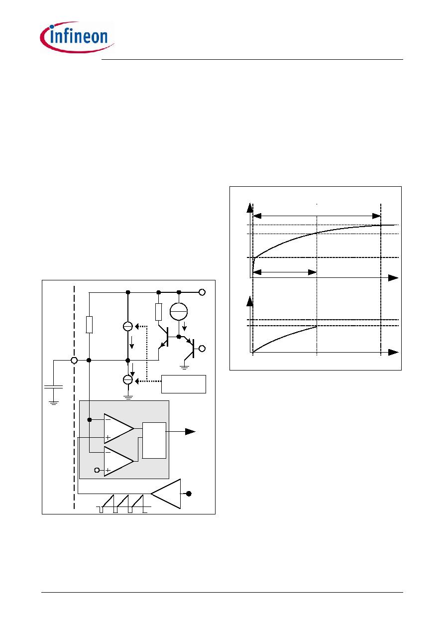
Power Management
Figure 3
Power Management
The Undervoltage Lockout monitors the external
supply voltage V
VCC
. When the SMPS is plugged to the
main line the internal Startup Cell is biased and starts
to charge the external capacitor C
VCC
which is
connected to the VCC pin. The VCC charge current
that is provided by the Startup Cell from the Drain pin is
1.05mA. When V
VCC
exceeds the on-threshold
V
CCon
=18V, bias circuit is switched on. Then the
Startup Cell is switched off by the Undervoltage
Lockout and therefore no power losses present due to
the connection of the Startup Cell to the Drain voltage.
To avoid uncontrolled ringing at switch-on a hysteresis
is implemented. The switch-off of the controller can
only take place after active mode was entered and
V
VCC
falls below 10.3V.
The maximum current consumption before the
controller is activated is about 300uA.
Internal Bias
Voltage
Reference
Power Management
5V
VCC
Undervoltage Lockout
18V
10.3
T1
Power-Down Reset
SoftS
Active Burst
Mode
Auto Restart
Mode
Startup Cell
Drain
CoolSETTM-F3
ICE3Bxx65J
Version 2.3
8
8 May 2006
When V
VCC
falls below the off-threshold V
CCoff
=10.3V
the bias circuit is switched off and the Power Down
reset let T1 discharging the soft-start capacitor C
SoftS
at
pin SoftS. Thus it is ensured that at every startup cycle
the voltage ramp at pin SoftS starts at zero.
The bias circuit is switched off if Auto Restart Mode is
entered. The current consumption is then reduced to
300uA.
Once the malfunction condition is removed, this block
will then turn back on. The recovery from Auto Restart
Mode does not require disconnecting the SMPS from
the AC line.
When Active Burst Mode is entered, some internal Bias
is switched off in order to reduce the current
consumption to about 500uA while keeping a
comparator (which trigger if V
FB
has exceeded 3.61V)
and the Soft Start capacitor clamped at 3.0 V as this is
necessary in this mode.
3.3
Startup Phase
Figure 4
Soft Start
At the beginning of the Startup Phase, the IC provides
a Soft Start duration whereby it controls the maximum
primary current by means of a duty cycle limitation. A
capacitor C
Softs
in combination with the internal pull up
resistor R
SoftS
determines the duty cycle until V
SoftS
exceeds 3.1V.
When the Soft Start begins, C
SoftS
is immediately
charged up to approx. 0.8V by T2. Therefore the Soft
Start Phase takes place between 0.8V and 3.1V.
Above V
SoftsS
= 3.1V there is no longer duty cycle
limitation DC
max
which is controlled by comparator C7
since comparator C2 blocks the gate G7 (see Figure
5).This maximum charge current in the very first stage
when V
SoftS
is below 0.8V, is limited to 0.9mA.
Figure 5
Startup Phase
By means of this extra charge stage, there is no delay
in the beginning of the Startup Phase when there is still
no switching. Furthermore Soft Start is finished at 3.1V
to have faster the maximum power capability. The duty
cycles DC
1
and DC
2
are depending on the mains and
the primary inductance of the transformer. The
limitation of the primary current by DC
2
is related to
V
SoftS
= 3.1V. But DC
1
is related to a maximum primary
current which is limited by the internal Current Limiting
with CS = 1V. Therefore the maximum Startup Phase
is divided into a Soft Start Phase until t1 and a phase
from t1 until t2 where maximum power is provided if
demanded by the FB signal.
Soft-Start
Comparator
Soft Start
&
G7
C7
C
SoftS
R
SoftS
T2
3.25k
5V
T3
0.8V
SoftS
Gate Driver
0.6V
x3.2
PWM OP
CS
3.1V
C2
Freq Jitter
Charging
current I
FJ
Freq Jitter
Discharging
current I
FJ
Freq Jitter
Control
DC
max
DC
1
DC
2
t
t
V
SoftS
max. Soft Start Phase
0.8V
3.1V
4.0V
max. Startup Phase
t1
t2
CoolSETTM-F3
ICE3Bxx65J
Version 2.3
9
8 May 2006
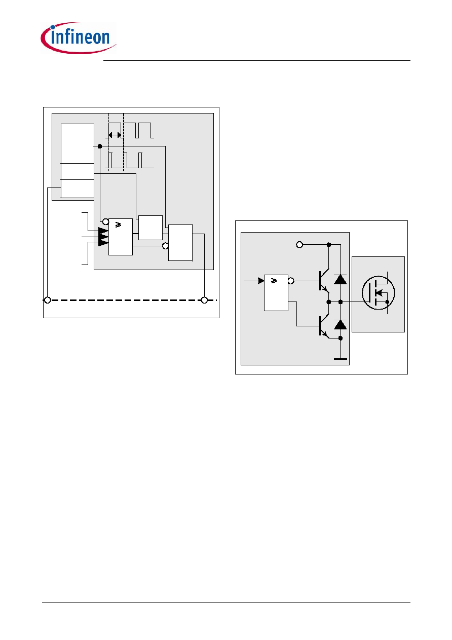
3.4
PWM Section
Figure 6
PWM Section
3.4.1
Oscillator and Jittering
The oscillator generates a fixed frequency with
frequency jittering of ±4% from the fixed frequency
(which is ±2.7kHz from 67kHz) at a jittering period T
FJ
.
The switching frequency is f
switch
= 67kHz.
A resistor, a capacitor and a current source and current
sink which determine the frequency are integrated. The
charging and discharging current of the implemented
oscillator capacitor are internally trimmed, in order to
achieve a very accurate switching frequency. The ratio
of controlled charge to discharge current is adjusted to
reach a maximum duty cycle limitation of D
max
=0.75.
Once the Soft Start period is over and when the IC goes
into normal mode, the Soft Start capacitor will be
charged and discharged through internal current
source, I
FJ
to generate a triangular waveform with a
jittering period T
FJ
which is externally adjustable by the
Soft Start capacitor, C
SoftS
(See Figure 4).
T
FJ
= k
FJ
* C
SoftS
where k
FJ
is a constant = 4 ms/uF
eg. T
FJ
= 4 ms if C
SoftS
= 1uF
3.4.2
PWM-Latch FF1
The oscillator clock output provides a set pulse to the
PWM-Latch when initiating the internal CoolMOSTM
conduction. After setting the PWM-Latch can be reset
by the PWM comparator, the Soft Start comparator or
the Current-Limit comparator. In case of resetting the
driver is shut down immediately.
3.4.3
Gate Driver
The Gate Driver is a fast totem pole gate drive which is
designed to avoid cross conduction currents.
The Gate Driver is active low at voltages below the
undervoltage lockout threshold V
VCCoff
.
Figure 7
Gate Driver
Oscillator
Duty
Cycle
max
Gate Driver
0.75
Clock
&
G9
1
G8
PWM Section
FF1
R
S
Q
Gate
Soft Start
Comparator
PWM
Comparator
Current
Limiting
Frequency
Jitter
SoftS
VCC
1
PWM-Latch
Depl. CoolMOSTM
Gate Driver
Gate

CoolSETTM-F3
ICE3Bxx65J
Version 2.3
10
8 May 2006
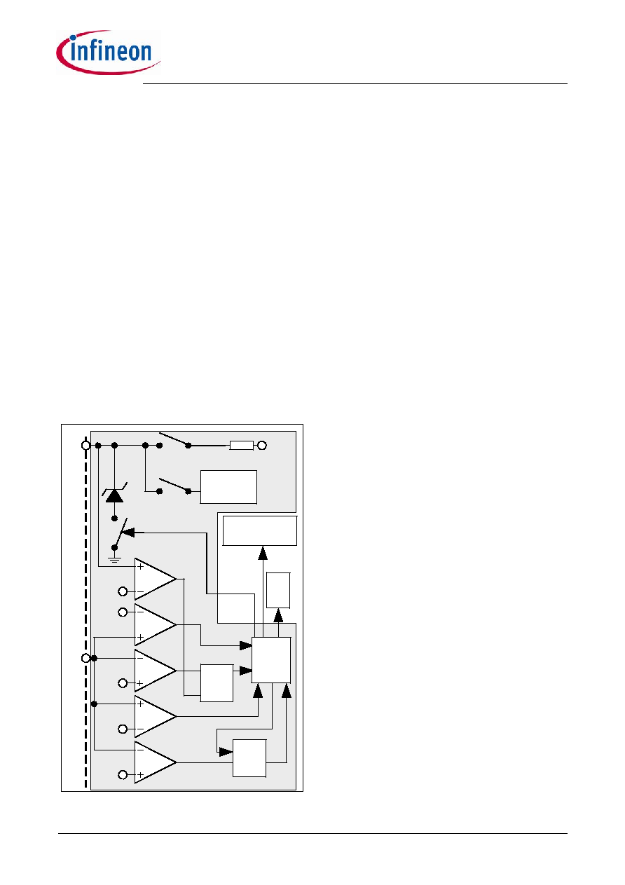
3.5
Current Limiting
Figure 8
Current Limiting
There is a cycle by cycle Current Limiting realized by
the Current-Limit comparator C10 to provide an
overcurrent detection. The source current of the
integrated Depl. CoolMOSTM is sensed via an external
sense resistor R
Sense
. By means of R
Sense
the source
current is transformed to a sense voltage V
Sense
which
is fed into the pin CS. If the voltage V
Sense
exceeds the
internal threshold voltage V
csth
the comparator C10
immediately turns off the gate drive by resetting the
PWM Latch FF1. A Propagation Delay Compensation
is added to support the immediate shut down without
delay of the integrated internal CoolMOSTM in case of
Current Limiting. The influence of the AC input voltage
on the maximum output power can thereby be avoided.
To prevent the Current Limiting from distortions caused
by leading edge spikes a Leading Edge Blanking is
integrated in the current sense path for the
comparators C10, C12 and the PWM-OP.
The output of comparator C12 is activated by the Gate
G10 if Active Burst Mode is entered. Once activated the
current limiting is thereby reduced to 0.32V. This
voltage level determines the power level when the
Active Burst Mode is left if there is a higher power
demand.
3.5.1
Leading Edge Blanking
Figure 9
Leading Edge Blanking
Each time when the integrated internal CoolMOSTM is
switched on a leading edge spike is generated due to
the primary-side capacitances and secondary-side
rectifier reverse recovery time. This spike can cause
the gate drive to switch off unintentionally. To avoid a
premature termination of the switching pulse, this spike
is blanked out with a time constant of t
LEB
= 220ns.
During this time, the gate drive will not be switched off.
3.5.2
Propagation Delay Compensation
In case of overcurrent detection, the switch-off of the
integrated internal CoolMOSTM is delayed due to the
propagation delay of the circuit. This delay causes an
overshoot of the peak current I
peak
which depends on
the ratio of dI/dt of the peak current (see Figure 10).
Figure 10
Current Limiting
The overshoot of Signal2 is bigger than of Signal1 due
to the steeper rising waveform. This change in the
slope is depending on the AC input voltage.
Propagation Delay Compensation is integrated to limit
the overshoot dependency on dI/dt of the rising primary
current. That means the propagation delay time
between exceeding the current sense threshold V
csth
and the switch off of the integrated inernal CoolMOSTM
is compensated over temperature within a wide range.
Current Limiting
C10
C12
&
0.32V
G10
Propagation-Delay
Compensation
V
csth
Active Burst
Mode
PWM Latch
FF1
10k
D1
1pF
PWM-OP
CS
Leading
Edge
Blanking
220ns
t
V
Sense
V
csth
t
LEB
= 220ns
t
I
Sense
I
Limit
t
Propagation Delay
I
Overshoot1
I
peak1
Signal1
Signal2
I
Overshoot2
I
peak2

CoolSETTM-F3
ICE3Bxx65J
Version 2.3
11
8 May 2006
Current Limiting is now possible in a very accurate way.
E.g. I
peak
= 0.5A with R
Sense
= 2. Without Propagation
Delay Compensation the current sense threshold is set
to a static voltage level V
csth
=1V. A current ramp of
dI/dt = 0.4A/µs, that means dV
Sense
/dt = 0.8V/µs, and a
propagation delay time of i.e. t
Propagation Delay
=180ns
leads then to an I
peak
overshoot of 14.4%. By means of
propagation delay compensation the overshoot is only
about 2% (see Figure 11).
Figure 11
Overcurrent Shutdown
The Propagation Delay Compensation is realized by
means of a dynamic threshold voltage V
csth
(see Figure
12). In case of a steeper slope the switch off of the
driver is earlier to compensate the delay.
Figure 12
Dynamic Voltage Threshold V
csth
3.6
Control Unit
The Control Unit contains the functions for Active Burst
Mode and Auto Restart Mode. The Active Burst Mode
and the Auto Restart Mode are combined with an
Adjustable Blanking Window which is depending on the
external Soft Start capacitor. By means of this
Adjustable Blanking Window, the IC avoids entering
into these two modes accidentally. Furthermore it also
provides a certain time whereby the overload detection
is delayed. This delay is useful for applications which
normally works with a low current and occasionally
require a short duration of high current.
3.6.1
Adjustable Blanking Window
Figure 13
Adjustable Blanking Window
V
SoftS
swings between 3.2V and 3.6V after the SMPS is
settled and S2 is on while S3 is off, this is due to the
frequency jittering function that is making use of the
Soft Start pin. If overload occurs V
FB
is exceeding 4.5V.
Auto Restart Mode can't be entered as the gate G5 is
still blocked by the comparator C3. But after V
FB
has
0,9
0,95
1
1,05
1,1
1,15
1,2
1,25
1,3
0
0,2
0,4
0,6
0,8
1
1,2
1,4
1,6
1,8
2
with compensation
without compensation
dt
dV
Sense
s
V
µ
Se
ns
e
V
V
t
V
csth
V
OSC
Signal1
Signal2
V
Sense
Propagation Delay
max. Duty Cycle
off time
t
C3
4.0V
C4
4.5V
C5
1.35V
&
G5
&
G6
3.0V
S1
Control Unit
Active
Burst
Mode
Auto
Restart
Mode
R
SoftS
5V
SoftS
FB
Frequency
Jitter
S2
S3
CoolSETTM-F3
ICE3Bxx65J
Version 2.3
12
8 May 2006
exceeded 4.5V the switch S2 is opened and S3 is
closed. The external Soft Start capacitor can now be
charged further by the integrated pull up resistor R
SoftS
via switch S3. The comparator C3 releases the gates
G5 and G6 once V
Softs
has exceeded 4.0V. Therefore
there is no entering of Auto Restart Mode possible
during this charging time of the external capacitor
C
SoftS
. The same procedure happens to the external
Soft Start capacitor if a low load condition is detected
by comparator C5 when V
FB
is falling below 1.35V.
Only after V
SoftS
has exceeded 4.0V and V
FB
is still
below 1.35V Active Burst Mode is entered.
3.6.2
Active Burst Mode
The controller provides Active Burst Mode for low load
conditions at V
OUT
. Active Burst Mode increases
significantly the efficiency at light load conditions while
supporting a low ripple on V
OUT
and fast response on
load jumps. During Active Burst Mode which is
controlled only by the FB signal the IC is always active
and can therefore immediately response on fast
changes at the FB signal. The Startup Cell is kept
switched off to avoid increased power losses for the
self supply.
Figure 14
Active Burst Mode
The Active Burst Mode is located in the Control Unit.
Figure 14 shows the related components.
3.6.2.1
Entering Active Burst Mode
The FB signal is always observed by the comparator
C5 if the voltage level falls below 1.35V. In that case the
switch S1 and S2 is released which allows the
capacitor C
SoftS
to be charged via S3 starting from the
swinging voltage level between 3.2V and 3.6V in
normal operating mode. If V
SoftS
exceeds 4.0V the
comparator C3 releases the gate G6 to enter the Active
Burst Mode. The time window that is generated by
combining the FB and SoftS signals with gate G6
avoids a sudden entering of the Active Burst Mode due
to large load jumps. This time window can be adjusted
by the external capacitor C
SoftS
.
After entering Active Burst Mode a burst flag is set and
the internal bias is switched off in order to reduce the
current consumption of the IC down to approx. 500uA.
Also, switch S1 is closed to clamped the Soft Start
voltage to 3.0V. In this Off State Phase the IC is no
longer self supplied so that therefore C
VCC
has to
provide the VCC current (see Figure 15). Furthermore
gate G11 is then released to start the next burst cycle
once V
FB
has 3.0V exceeded.
It has to be ensured by the application that the VCC
remains above the Undervoltage Lockout Level of
10.3V to avoid that the Startup Cell is accidentally
switched on. Otherwise power losses are significantly
increased. The minimum VCC level during Active Burst
Mode is depending on the load conditions and the
application. The lowest VCC level is reached at no load
conditions at V
OUT
.
3.6.2.2
Working in Active Burst Mode
After entering the Active Burst Mode the FB voltage
rises as V
OUT
starts to decrease due to the inactive
PWM section. Comparator C6a observes the FB signal
if the voltage level 3.61V is exceeded. In that case the
internal circuit is again activated by the internal Bias to
start with switching. As now in Active Burst Mode the
gate G10 is released the current limit is only 0.32V to
reduce the conduction losses and to avoid audible
noise. If the load at V
OUT
is still below the starting level
for the Active Burst Mode the FB signal decreases
down to 3.0V. At this level C6b deactivates again the
internal circuit by switching off the internal Bias. The
gate G11 is released as after entering Active Burst
Mode the burst flag is set. If working in Active Burst
Mode the FB voltage is changing like a saw tooth
between 3.0V and 3.61V (see figure 15).
3.6.2.3
Leaving Active Burst Mode
The FB voltage immediately increases if there is a high
load jump. This is observed by comparator C4. As the
current limit is ca. 32% during Active Burst Mode a
certain load jump is needed that FB can exceed 4.5V.
At this time C4 resets the Active Burst Mode which also
C3
4.0V
C4
4.5V
C6a
3.61V
C5
1.35V
FB
Control Unit
Active
Burst
Mode
3.0V
S1
Internal Bias
R
SoftS
5V
SoftS
&
G10
Current
Limiting
&
G6
C6b
3.0V
&
G11
Frequency
Jitter
S2
S3

CoolSETTM-F3
ICE3Bxx65J
Version 2.3
13
8 May 2006
blocks C12 by the gate G10. Maximum current can now
be provided to stabilize V
OUT
.
Figure 15
Signals in Active Burst Mode
3.6.3
Protection Modes
The IC provides several protection features that
increase the SMPS system's robustness and safety.
The following table shows the possible system failures
and the corresponding protection modes.
3.6.3.1
Auto Restart Mode I
Figure 16
Auto Restart Mode I
The VCC voltage is observed by comparator C13 if
20.5V is exceeded. The output of C13 is combined with
both the output of C3 which checks for V
SoftS
< 4.0V and
the output of C4 which checks for V
FB
> 4.5V. Therefore
the overvoltage detection can only be active during Soft
Start Phase (V
SoftS
< 4.0V) and when FB signal is
outside the operating range > 4.5V. This means any
1.35V
3.61V
4.5V
V
FB
3.0V
4.0V
V
SoftS
t
t
0.32V
1.0V
V
CS
10.3V
V
VCC
t
t
500uA
I
VCC
t
2mA
V
OUT
t
Max. Ripple < 1%
Blanking Window
Current limit level
during Active Burst
Mode
3.0V
Entering
Active Burst
Mode
Leaving
Active Burst
Mode
3.6V~
3.2V
VCC Overvoltage
Auto Restart Mode I
Over temperature
Auto Restart Mode I
Overload
Auto Restart Mode II
Open Loop
Auto Restart Mode II
VCC Undervoltage
Auto Restart Mode II
Short Optocoupler
Auto Restart Mode II
C3
Spike
Blanking
8.0us
Thermal Shutdown
T
j
>140∞C
Auto
Restart
Mode
Internal
Bias
Control Unit
C13
20.5V
VCC
C4
4.5V
FB
4.0V
SoftS
&
G12
&
G13
FF2
R
S
Q
UVLO
CoolSETTM-F3
ICE3Bxx65J
Version 2.3
14
8 May 2006
small voltage overshoots of V
VCC
during normal
operating cannot trigger the Auto Restart Mode I.
In Order to ensure system reliability and prevent any
false activation, a blanking time is implemented before
the IC can enter into the Auto Restart Mode I. The
output of the VCC overvoltage detection is fed into a
spike blanking with a time constant of 8.0us.
The other fault detection which can result in the Auto
Restart Mode I and has this 8.0us blanking time is the
Overtemperature detection. This block checks for a
junction temperature of higher than 140∞C for
malfunction operation.
Once Auto Restart Mode is entered, the internal bias is
switched off in order to reduce the current consumption
of the IC as much as possible. In this mode, the
average current consumption is only 300uA as the only
working blocks are the reference block and the
Undervoltage Lockout(UVLO) which controls the
Startup Cell by switching on/off at V
VCCon
/V
VCCoff
.
As there is no longer a self supply by the auxiliary
winding, VCC starts to drop. The UVLO switches on the
integrated Startup Cell when VCC falls below 10.3V. It
will continue to charge VCC up to 18V whereby it is
switched off again and the IC enters into the Start Up
Phase.
As long as all fault conditions have been removed, the
IC will automatically power up as usual with switching
cycle at the GATE output after Soft Start duration. Thus
the name Auto Restart Mode.
3.6.3.2
Auto Restart Mode II
Figure 17
Auto Restart Mode II
In case of Overload or Open Loop, FB exceeds 4.5V
which will be observed by C4. At this time, the external
Soft Start capacitor can now be charged further by the
integrated pull up resistor R
SoftS
via switch S3 (see
Figure 13). If V
SoftS
exceeds 4.0V which is observed by
C3, Auto Restart Mode II is entered as both inputs of
the gate G5 are high.
This charging of the Soft Start capacitor from
3.2V~3.6V to 4.0V defines a blanking window which
prevents the system from entering into Auto Restart
Mode II unintentionally during large load jumps. In this
event, FB will rise close to 5.0V for a short duration
before the loop regulates with FB less than 4.5V. This
is the same blanking time window as for the Active
Burst Mode and can therefore be adjusted by the
external C
SoftS
.
In case of VCC undervoltage, ie. VCC falls below
10.3V, the IC will be turned off with the Startup Cell
charging VCC as described earlier in this section. Once
VCC is charged above 18V, the IC will start a new
startup cycle. The same procedure applies when the
system is under Short Optocoupler fault condition, as it
will lead to VCC undervoltage.
C3
4.0V
C4
4.5V
&
G5
Control Unit
SoftS
Internal
Bias
Auto
Restart
Mode
FB
CoolSETTM-F3
ICE3Bxx65J
Version 2.3
15
8 May 2006
4
Electrical Characteristics
Note:
All voltages are measured with respect to ground (Pin 8). The voltage levels are valid if other ratings are
not violated.
4.1
Absolute Maximum Ratings
Note:
Absolute maximum ratings are defined as ratings, which when being exceeded may lead to destruction
of the integrated circuit. For the same reason make sure, that any capacitor that will be connected to pin 7
(VCC) is discharged before assembling the application circuit.
Parameter
Symbol
Limit Values
Unit
Remarks
min.
max.
Drain Source Voltage
V
DS
-
650
V
T
j
= 110∞C
Pulse drain current,
t
p
limited by max.
T
j
=150∞C
ICE3B0365J
I
D_Puls1
-
0.9
A
ICE3B0565J
I
D_Puls2
-
1.6
A
ICE3B1565J
I
D_Puls3
-
6.1
A
Avalanche energy,
repetitive t
AR
limited
by max. T
j
=150∞C
1)
1)
Repetetive avalanche causes additional power losses that can be calculated as P
AV
=E
AR
* f
ICE3B0365J
E
AR1
-
0.005
mJ
ICE3B0565J
E
AR2
-
0.01
mJ
ICE310565J
E
AR3
-
0.15
mJ
Avalanche current,
repetitive t
AR
limited
by max. T
j
=150∞C
1)
ICE3B0365J
I
AR1
-
0.3
A
ICE3B0565J
I
AR2
-
0.5
A
ICE3B1565J
I
AR3
-
1.5
A
VCC Supply Voltage
V
VCC
-0.3
27
V
FB Voltage
V
FB
-0.3
5.0
V
SoftS Voltage
V
SoftS
-0.3
5.0
V
CS Voltage
V
CS
-0.3
5.0
V
Junction Temperature
T
j
-40
150
∞C
Controller & CoolMOSTM
Storage Temperature
T
S
-55
150
∞C
Thermal Resistance
Junction-Ambient
R
thJA
-
90
K/W
PG-DIP-8-6
ESD Capability
V
ESD
-
2
kV
Human body model
2)
2)
According to EIA/JESD22-A114-B (discharging a 100pF capacitor through a 1.5k
series resistor)

Version 2.3
16
8 May 2006
CoolSETTM-F3
ICE3Bxx65J
4.2
Operating Range
Note:
Within the operating range the IC operates as described in the functional description.
4.3
Characteristics
4.3.1
Supply Section
Note:
The electrical characteristics involve the spread of values guaranteed within the specified supply voltage
and junction temperature range T
J
from ≠ 25
o
C to 130
o
C. Typical values represent the median values,
which are related to 25∞C. If not otherwise stated, a supply voltage of V
CC
= 18 V is assumed.
Parameter
Symbol
Limit Values
Unit
Remarks
min.
max.
VCC Supply Voltage
V
VCC
V
VCCoff
26
V
Junction Temperature of Controller
T
jCon
-25
130
∞C
Max value limited due to
integrated thermal shut down
Junction Temperature of
CoolMOSTM
T
JCoolMOS
-25
150
∞C
Parameter
Symbol
Limit Values
Unit
Test Condition
min.
typ.
max.
Start Up Current
I
VCCstart
-
300
450
µA
V
VCC
= 17V
VCC Charge Current
I
VCCcharge1
5.0
mA
V
VCC
= 0V
I
VCCcharge2
0.55
1.05
1.60
mA
V
VCC
= 1V
I
VCCcharge3
-
0.88
-
mA
V
VCC
= 17V
Leakage Current of
Start Up Cell & CoolMOS
I
StartLeak
-
0.2
50
µA
V
Drain
= 450V
at T
j
= 100∞C
Supply Current with
Inactive Gate
I
VCCsup_ng
-
1.7
2.5
mA
Soft Start pin is open
Supply Current with Active Gate I
VCCsup_g
-
2.5
3.6
mA
V
SoftS
= 3.0V
I
FB
= 0
Supply Current in
Auto Restart Mode
with Inactive Gate
I
VCCrestart
-
300
-
µA
I
FB
= 0
I
Softs
= 0
Supply Current in
Active Burst Mode
with Inactive Gate
I
VCCburst1
-
500
950
uA
V
FB
= 2.5V
V
SoftS
= 3.0V
I
VCCburst2
-
500
950
uA
V
VCC
= 11.5V
V
FB
= 2.5V
V
SoftS
= 3.0V
VCC Turn-On Threshold
VCC Turn-Off Threshold
VCC Turn-On/Off Hysteresis
V
VCCon
V
VCCoff
V
VCChys
17.0
9.6
-
18.0
10.3
7.7
19.0
11.0
-
V
V
V
CoolSETTM-F3
ICE3Bxx65J
Version 2.3
17
8 May 2006
4.3.2
Internal Voltage Reference
4.3.3
PWM Section
4.3.4
Control Unit
Parameter
Symbol
Limit Values
Unit
Test Condition
min.
typ.
max.
Trimmed Reference Voltage
V
REF
4.90
5.00
5.10
V
measured at pin FB
I
FB
= 0
Parameter
Symbol
Limit Values
Unit
Test Condition
min.
typ.
max.
Fixed Oscillator Frequency
f
OSC3
58
67
76
kHz
f
OSC4
62
67
74.5
kHz
T
j
= 25∞C
Frequency Jittering Range
f
delta
-
±2.7
-
kHz
T
j
= 25∞C
Max. Duty Cycle
D
max
0.70
0.75
0.80
Min. Duty Cycle
D
min
0
-
-
V
FB
< 0.3V
PWM-OP Gain
A
V
3.0
3.2
3.4
Max. Level of Voltage Ramp
V
Max-Ramp
-
0.6
-
V
V
FB
Operating Range Min Level V
FBmin
-
0.5
-
V
V
FB
Operating Range Max level V
FBmax
-
-
4.3
V
CS=1V limited by
Comparator C4
1)
1)
This parameter is not subject to production test - verified by design/characterization
Feedback Pull-Up Resistor
R
FB
9
14
22
k
Soft-Start Pull-Up Resistor
R
SoftS
30
45
62
k
Parameter
Symbol
Limit Values
Unit
Test Condition
min.
typ.
max.
Deactivation Level for SoftS
Comparator C7 by C2
V
SoftSC2
2.98
3.10
3.22
V
V
FB
= 5V
Clamped V
SoftS
Voltage during
Burst Mode
V
SoftSclmp_bm
2.88
3.00
3.12
V
Activation Limit of
Comparator C3
V
SoftSC3
3.85
4.00
4.15
V
V
FB
= 5V
SoftS Startup Current
I
SoftSstart
-
0.9
-
mA
V
SoftS
= 0V
Over Load & Open Loop
Detection Limit for
Comparator C4
V
FBC4
4.33
4.50
4.67
V
V
SoftS
= 4.5V
Active Burst Mode Level for
Comparator C5
V
FBC5
1.23
1.35
1.43
V
V
SoftS
= 4.5V
Active Burst Mode Level for
Comparator C6a
V
FBC6a
3.48
3.61
3.76
V
After Active Burst
Mode is entered

Version 2.3
18
8 May 2006
CoolSETTM-F3
ICE3Bxx65J
Note:
The trend of all the voltage levels in the Control Unit is the same regarding the deviation except V
VCCOVP
4.3.5
Current Limiting
4.3.6
CoolMOSTM Section
Active Burst Mode Level for
Comparator C6b
V
FBC6b
2.88
3.00
3.12
V
After Active Burst
Mode is entered
Overvoltage Detection Limit
V
VCCOVP
19.5
20.5
21.5
V
V
FB
= 5V, V
SoftS
= 3V
Thermal Shutdown
1)
T
jSD
130
140
150
∞C
Spike Blanking
t
Spike
-
8.0
-
µs
1)
The parameter is not subject to production test - verified by design/characterization
Parameter
Symbol
Limit Values
Unit
Test Condition
min.
typ.
max.
Peak Current Limitation (incl.
Propagation Delay Time)
(see Figure 11)
V
csth
1.01
1.06
1.11
V
dV
sense
/ dt = 0.6V/
µs
Peak Current Limitation during
Active Burst Mode
V
CS2
0.27
0.32
0.37
V
Leading Edge Blanking
t
LEB
-
220
-
ns
V
SoftS
= 3.0V
CS Input Bias Current
I
CSbias
-1.0
-0.2
0
µA
V
CS
= 0V
Parameter
Symbol
Limit Values
Unit
Test Condition
min.
typ.
max.
Drain Source Breakdown
Voltage
V
(BR)DSS
600
650
-
-
-
-
V
V
T
j
= 25∞C
T
j
= 110∞C
Drain Source
On-Resistance
ICE3B0365J
R
DSon1
-
-
6.45
13.70
7.50
17.00
T
j
= 25∞C
T
j
= 125∞C
1)
at I
D
= 0.3A
1)
The parameter is not subject to production test - verified by design/characterization
ICE3B0565J
R
DSon2
-
-
4.70
10.00
5.44
12.50
T
j
= 25∞C
T
j
= 125∞C
1)
at I
D
= 0.5A
ICE3B1565J
R
DSon3
-
-
1.70
3.57
1.96
4.12
T
j
= 25∞C
T
j
= 125∞C
1)
at I
D
= 1.5A
Effective output
capacitance,
energy related
ICE3B0365J
C
o(er)1
-
3.65
-
pF
V
DS
= 0V to 480V
ICE3B0565J
C
o(er)2
-
4.75
-
pF
ICE3B1565J
C
o(er)3
-
11.63
-
pF
Rise Time
t
rise
-
30
2)
2)
Measured in a Typical Flyback Converter Application
-
ns
Fall Time
t
fall
-
30
2)
-
ns
CoolSETTM-F3
ICE3Bxx65J
Version 2.3
19
8 May 2006
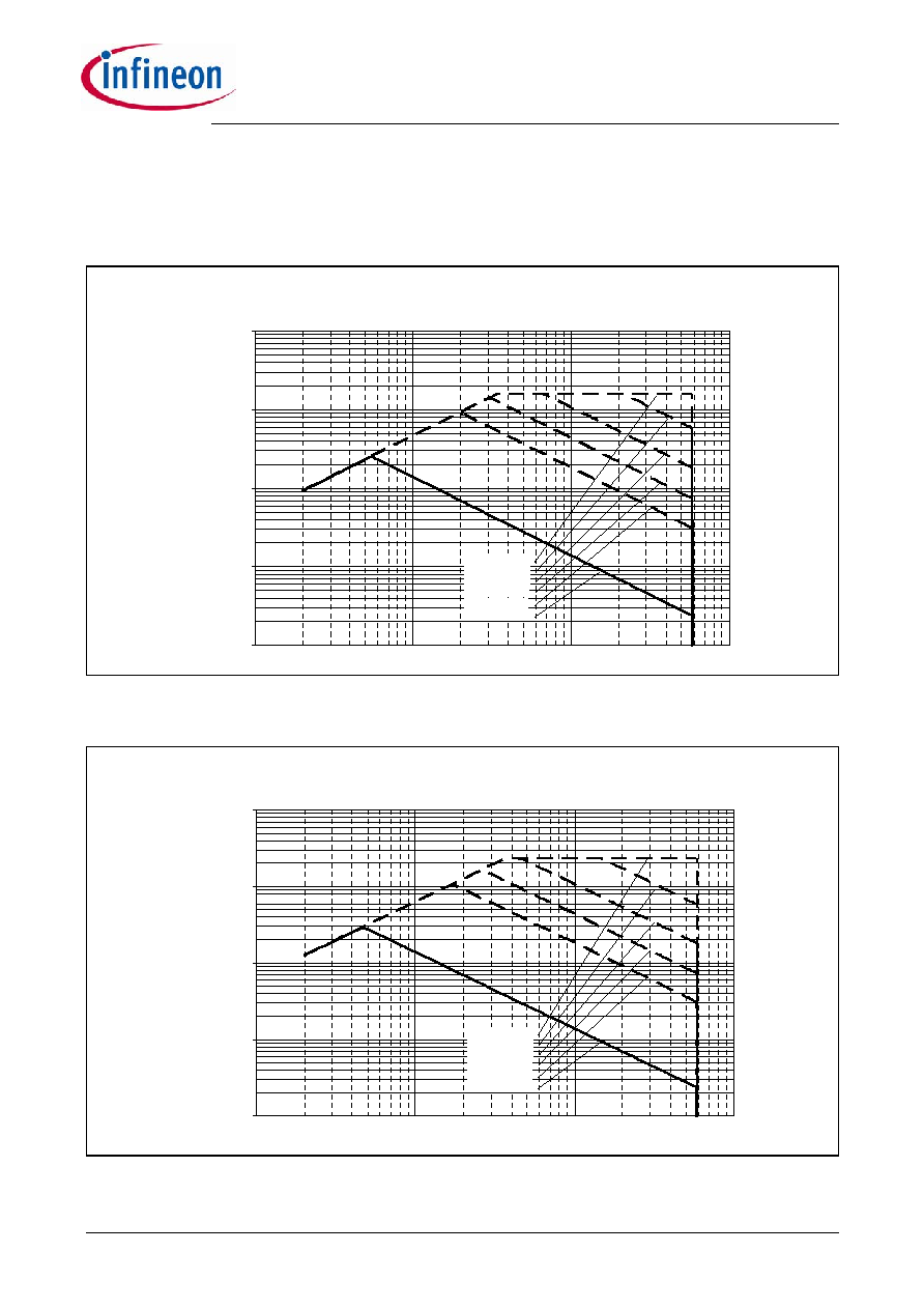
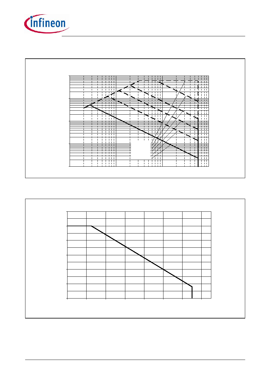
5
Temperature derating curve
Figure 18 Safe Operating area ( SOA ) curve for ICE3B0565J
Figure 19 Safe Operating area ( SOA ) curve for ICE3B0565J
Safe Operating Area for ICE3A(B)0365(J)
I
D
= f ( V
DS
)
parameter : D = 0, T
C
= 25deg.C
0.001
0.01
0.1
1
10
1
10
100
1000
V
DS
[V]
I
D
[A
]
DC
tp = 10ms
tp = 0.01ms
tp = 0.1ms
tp = 1ms
tp = 100ms
Safe Operating Area for ICE3A(B)0565(J)
I
D
= f ( V
DS
)
parameter : D = 0, T
C
= 25deg.C
0.001
0.01
0.1
1
10
1
10
100
1000
V
DS
[V]
I
D
[A]
DC
tp = 100ms
tp = 0.1ms
tp = 1ms
tp = 10ms
tp = 1000ms
Version 2.3
20
8 May 2006
CoolSETTM-F3
ICE3Bxx65J
Figure 20 Safe Operating area ( SOA ) curve for ICE3B1565J
Figure 21 SOA temperature derating coefficient curve
Safe Operating Area for ICE3A(B)1565(J)
I
D
= f ( V
DS
)
parameter : D = 0, T
C
= 25deg.C
0.001
0.01
0.1
1
10
1
10
100
1000
V
DS
[V]
I
D
[A]
DC
tp = 100ms
tp = 0.1ms
tp = 1ms
tp = 10ms
tp = 1000ms
SOA temperature derating coefficient curve for F3 & F2 CoolSET
0
20
40
60
80
100
120
0
20
40
60
80
100
120
140
Junction temperature Tc [deg.C]
S
O
A
t
e
mper
at
ure der
a
t
i
n
g c
oef
f
i
c
i
en
t
[
%
]

CoolSETTM-F3
ICE3Bxx65J
Version 2.3
21
8 May 2006
6
Outline Dimension
Figure 22 PG-DIP-8-6 ( Pb-free lead plating Platic Dual-in-Line Outline )
Dimensions in mm
PG-DIP-8-6
(Plastic Dual In-Line Outline)

Version 2.3
22
8 May 2006
CoolSETTM-F3
ICE3Bxx65J
7
Marking
Figure 23 Marking for ICE3B0365J
Figure 24 Marking for ICE3B0565J
Marking
Marking

CoolSETTM-F3
ICE3Bxx65J
Version 2.3
23
8 May 2006
Figure 25 Marking for ICE3B1565J
Marking
Version 2.3
24
8 May 2006
CoolSETTM-F3
ICE3Bxx65J
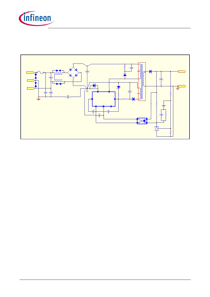
Schematic for recommended PCB layout
8
Schematic for recommended PCB layout
Figure 26 Schematic for recommended PCB layout
General guideline for PCB layout design using F3 CoolSET (refer to Figure 26):
1. "Star Ground "at bulk capacitor ground, C11:
"Star Ground "means all primary DC grounds should be connected to the ground of bulk capacitor C11
separately in one point. It can reduce the switching noise going into the sensitive pins of the CoolSET device
effectively. The primary DC grounds include the followings.
a. DC ground of the primary auxiliary winding in power transformer, TR1, and ground of C16 and Z11.
b. DC ground of the current sense resistor, R12
c. DC ground of the CoolSET device, GND pin of IC11; the signal grounds from C13, C14, C15 and collector of
IC12 should be connected to the GND pin of IC11 and then "star "connect to the bulk capacitor ground.
d. DC ground from bridge rectifier, BR1
e. DC ground from the bridging Y-capacitor, C4
2. High voltage traces clearance:
High voltage traces should keep enough spacing to the nearby traces. Otherwise, arcing would incur.
a. 400V traces (positive rail of bulk capacitor C11) to nearby trace: > 2.0mm
b. 600V traces (drain voltage of CoolSET IC11) to nearby trace: > 2.5mm
3. Filter capacitor close to the controller ground:
Filter capacitors, C13, C14 and C15 should be placed as close to the controller ground and the controller pin
as possible so as to reduce the switching noise coupled into the controller.
Guideline for PCB layout design when >3KV lightning surge test applied (refer to Figure 26):
1. Add spark gap
Spark gap is a pair of saw-tooth like copper plate facing each other which can discharge the accumulated
charge during surge test through the sharp point of the saw-tooth plate.
a. Spark Gap 3 and Spark Gap 4, input common mode choke, L1:
Gap separation is around 1.5mm (no safety concern)
C11
bulk cap
R11
D11
C12
IC12
R12
C13
C16
C15
C14
D13
R14
R23
R22
IC21
C23
R24
C22
R21
R25
GND
Vo
D21
C21
F3 CoolSET schematic for recommended PCB layout
R13
Z11
TR1
N
L
BR1
C2
Y-CAP
C3
Y-CAP
C1
X-CAP
L1
FUSE1
C4
Y-CAP
GND
Spark Gap 3
Spark Gap 4
D11
Spark Gap 1
Spark Gap 2
FB
CS
GND
NC
SOFTS/BL
VCC
F3
DRAIN
CoolSET
IC11
*

CoolSETTM-F3
ICE3Bxx65J
Schematic for recommended PCB layout
Version 2.3
25
8 May 2006
b. Spark Gap 1 and Spark Gap 2, Live / Neutral to GROUND:
These 2 Spark Gaps can be used when the lightning surge requirement is >6KV.
230Vac input voltage application, the gap separation is around 5.5mm
115Vac input voltage application, the gap separation is around 3mm
2. Add Y-capacitor (C2 and C3) in the Live and Neutral to ground even though it is a 2-pin input
3. Add negative pulse clamping diode, D11 to the Current sense resistor, R12:
The negative pulse clamping diode can reduce the negative pulse going into the CS pin of the CoolSET and
reduce the abnormal behavior of the CoolSET. The diode can be a fast speed diode such as IN4148.
The principle behind is to drain the high surge voltage from Live/Neutral to Ground without passing through the
sensitive components such as the primary controller, IC11.

Qualit‰t hat f¸r uns eine umfassende
Bedeutung. Wir wollen allen Ihren
Anspr¸chen in der bestmˆglichen
Weise gerecht werden. Es geht uns also
nicht nur um die Produktqualit‰t ≠
unsere Anstrengungen gelten
gleichermaþen der Lieferqualit‰t und
Logistik, dem Service und Support
sowie allen sonstigen Beratungs- und
Betreuungsleistungen.
Dazu gehˆrt eine bestimmte
Geisteshaltung unserer Mitarbeiter.
Total Quality im Denken und Handeln
gegen¸ber Kollegen, Lieferanten und
Ihnen, unserem Kunden. Unsere
Leitlinie ist jede Aufgabe mit ,,Null
Fehlern" zu lˆsen ≠ in offener
Sichtweise auch ¸ber den eigenen
Arbeitsplatz hinaus ≠ und uns st‰ndig
zu verbessern.
Unternehmensweit orientieren wir uns
dabei auch an ,,top" (Time Optimized
Processes), um Ihnen durch grˆþere
Schnelligkeit den entscheidenden
Wettbewerbsvorsprung zu verschaffen.
Geben Sie uns die Chance, hohe
Leistung durch umfassende Qualit‰t zu
beweisen.
Wir werden Sie ¸berzeugen.
Quality takes on an allencompassing
significance at Semiconductor Group.
For us it means living up to each and
every one of your demands in the best
possible way. So we are not only
concerned with product quality. We
direct our efforts equally at quality of
supply and logistics, service and
support, as well as all the other ways in
which we advise and attend to you.
Part of this is the very special attitude of
our staff. Total Quality in thought and
deed, towards co-workers, suppliers
and you, our customer. Our guideline is
"do everything with zero defects", in an
open manner that is demonstrated
beyond your immediate workplace, and
to constantly improve.
Throughout the corporation we also
think in terms of Time Optimized
Processes (top), greater speed on our
part to give you that decisive
competitive edge.
Give us the chance to prove the best of
performance through the best of quality
≠ you will be convinced.
h t t p : / / w w w . i n f i n e o n . c o m
Total Quality Management
Published by Infineon Technologies AG