 | ÐлекÑÑоннÑй компоненÑ: IDP15E60 | СкаÑаÑÑ:  PDF PDF  ZIP ZIP |
Äîêóìåíòàöèÿ è îïèñàíèÿ www.docs.chipfind.ru
19.05.2000
Page 1
HITFET
====
BTS 141
Smart Lowside Power Switch
Features
· Logic Level Input
· Input Protection (ESD)
·=Thermal shutdown with latch
· Overload protection
· Short circuit protection
· Overvoltage protection
·
Current limitation
· Status feedback with external input resistor
· Analog driving possible
Product Summary
Drain source voltage
V
DS
60
V
On-state resistance
R
DS(on)
28
m
Current limit
I
D(lim)
25
A
Nominal load current
I
D(ISO)
12
A
Clamping energy
E
AS
4000 mJ
Application
· All kinds of resistive, inductive and capacitive loads in switching or
linear applications
· µC compatible power switch for 12 V and 24 V DC applications
· Replaces electromechanical relays and discrete circuits
General Description
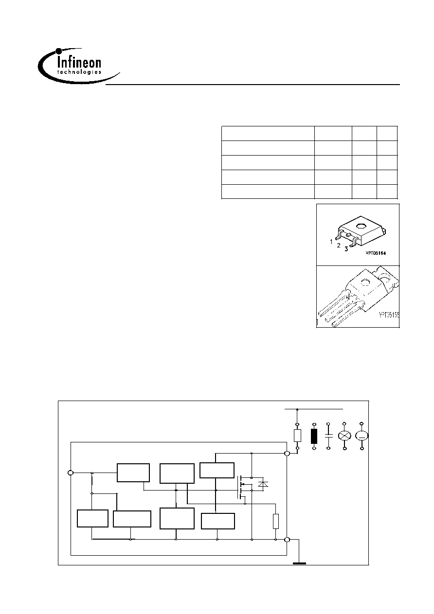
N channel vertical power FET in Smart SIPMOS chip on chip tech-
nology. Fully protected by embedded protected functions.
p rotection
O ve rvoltag e
D rain
IN
E S D
H IT F E T
S o u rce
C u rre n t
1
3
O ve r-
p ro te ctio n
te m pe rature
S h ort circ uit
p ro te ctio n
+
dv /d t
lim ita tio n
lim ita tio n
V bb
S ho rt c ircu it
p rotection
L O A D
2
O v erloa d
pro te ctio n
M

19.05.2000
Page 2
BTS 141
Maximum Ratings at Tj = 25 °C unless otherwise specified
Parameter
Symbol
Value
Unit
Drain source voltage
V
DS
60
V
Drain source voltage for short circuit protection
V
DS(SC)
32
Continuous input current
1)
-0.2V
V
IN
10V
V
IN
< -0.2V or V
IN
> 10V
I
IN
no limit
| I
IN
|
2
mA
Operating temperature
T
j
- 40 ... +150
°C
Storage temperature
T
stg
- 55 ... +150
Power dissipation
T
C
= 25 °C
P
tot
149
W
Unclamped single pulse inductive energy
I
D(ISO)
= 12 A
E
AS
4000
mJ
Electrostatic discharge voltage
(Human Body Model)
according to MIL STD 883D, method 3015.7 and
EOS/ESD assn. standard S5.1 - 1993
V
ESD
3000
V
Load dump protection V
LoadDump
2)
= V
A
+ V
S
V
IN
=low or high; V
A
=13.5 V
t
d
= 400 ms, R
I
= 2
, I
D
=0,5*12A
t
d
= 400 ms, R
I
= 2
, I
D
= 12A
V
LD
100
84
DIN humidity category, DIN 40 040
E
IEC climatic category; DIN IEC 68-1
40/150/56
Thermal resistance
junction - case:
R
thJC
0.84
K/W
junction - ambient:
R
thJA
75
SMD version, device on PCB:
3)
R
thJA
45
1In case of thermal shutdown a minimum sensor holding current of 500 µA has to be guaranteed (see also page 3).
2VLoaddump is setup without the DUT connected to the generator per ISO 7637-1 and DIN 40839
3 Device on 50mm*50mm*1.5mm epoxy PCB FR4 with 6cm 2 (one layer, 70µm thick) copper area for Drain connection.
PCB mounted vertical without blown air.

19.05.2000
Page 3
BTS 141
Electrical Characteristics
Parameter
Symbol
Values
Unit
at T
j
=25°C, unless otherwise specified
min.
typ.
max.
Characteristics
Drain source clamp voltage
T
j
= - 40 ...+ 150°C, I
D
= 10 mA
V
DS(AZ)
60
-
73
V
Off state drain current
V
DS
= 32 V, T
j
= -40...+150 °C, V
IN
= 0 V
I
DSS
-
-
20
µA
Input threshold voltage
I
D
= 2,7 mA
V
IN(th)
1.3
1.7
2.2
V
Input current - normal operation, I
D
<I
D(lim)
:
V
IN
= 10 V
I
IN(1)
-
35
100
µA
Input current - current limitation mode, I
D
=I
D(lim)
:
V
IN
= 10 V
I
IN(2)
-
270
500
Input current - after thermal shutdown, I
D
=0 A:
V
IN
= 10 V
I
IN(3)
1000
2500
4000
Input holding current after thermal shutdown
1)
T
j
= 25 °C
T
j
= 150 °C
I
IN(H)
500
300
-
-
-
-
On-state resistance
V
IN
= 5 V, I
D
= 12 A, T
j
= 25 °C
V
IN
= 5 V, I
D
= 12 A, T
j
= 150 °C
R
DS(on)
-
-
31
52
34
68
m
On-state resistance
V
IN
= 10 V, I
D
= 12 A, T
j
= 25 °C
V
IN
= 10 V, I
D
= 12 A, T
j
= 150 °C
R
DS(on)
-
-
25
45
28
56
Nominal load current (ISO 10483)
V
IN
= 10 V, V
DS
= 0.5 V, T
C
= 85 °C
I
D(ISO)
12
-
-
A
1If the input current is limited by external components, low drain currents can flow and heat the device.
Auto restart behaviour can occur.

19.05.2000
Page 4
BTS 141
Electrical Characteristics
Parameter
Symbol
Values
Unit
at T
j
=25°C, unless otherwise specified
min.
typ.
max.
Characteristics
Initial peak short circuit current limit
V
IN
= 10 V, V
DS
= 12 V
I
D(SCp)
-
100
-
A
Current limit
1)
V
IN
= 10 V, V
DS
= 12 V, t
m
= 350 µs,
T
j
= -40...+150 °C
I
D(lim)
25
35
50
Dynamic Characteristics
Turn-on time V
IN
to 90% I
D
:
R
L
= 2,2
, V
IN
= 0 to 10 V, V
bb
= 12 V
t
on
-
40
100
µs
Turn-off time V
IN
to 10% I
D
:
R
L
= 2,2
, V
IN
= 10 to 0 V, V
bb
= 12 V
t
off
-
70
170
Slew rate on 70 to 50% V
bb
:
R
L
= 2,2
, V
IN
= 0 to 10 V, V
bb
= 12 V
-dV
DS
/dt
on
-
1
3
V/µs
Slew rate off 50 to 70% V
bb
:
R
L
= 2,2
, V
IN
= 10 to 0 V, V
bb
= 12 V
dV
DS
/dt
off
-
1
3
Protection Functions
Thermal overload trip temperature
T
jt
150
165
-
°C
Unclamped single pulse inductive energy
I
D
= 12 A, T
j
= 25 °C, V
bb
= 32 V
I
D
= 12 A, T
j
= 150 °C, V
bb
= 32 V
E
AS
4000
900
-
-
-
-
mJ
Inverse Diode
Inverse diode forward voltage
I
F
= 5*12A, t
m
= 300
µS, V
IN
= 0 V
V
SD
-
1.13
-
V
1Device switched on into existing short circuit (see diagram Determination of I D(lim)). If the device is in on condition
and a short circuit occurs, these values might be exceeded for max. 50 µs.
19.05.2000
Page 5
BTS 141
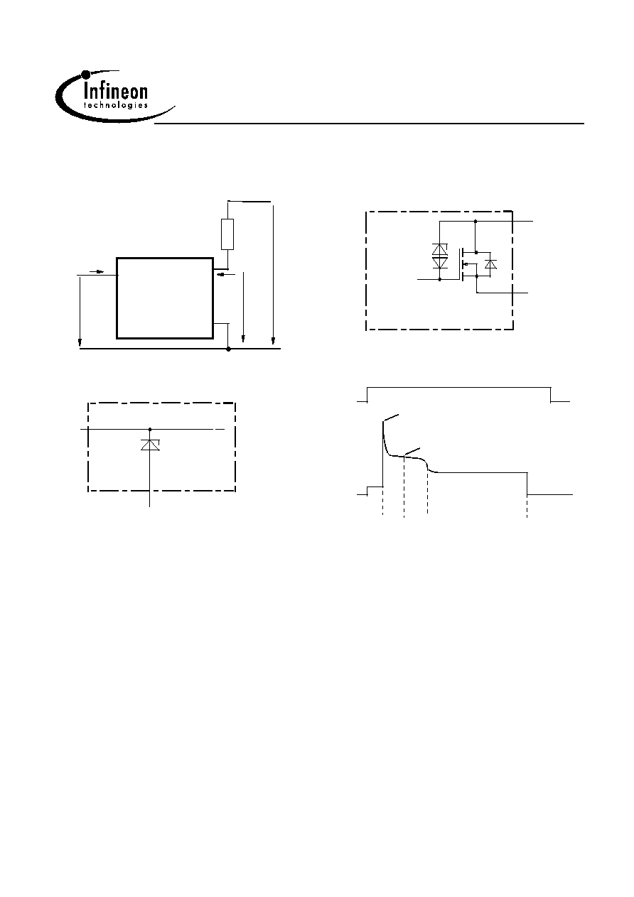
Block Diagramm
Terms
Inductive and overvoltage output clamp
HITFET
IN
D
VIN
ID
VDS
1
IIN
S
Vbb
RL
2
3
HITFET
VZ
D
S
Short circuit behaviour
V IN
ID
I D(SCp)
t 0
tm
t 2
ID(Lim)
t 1
Input circuit (ESD protection)
IN
ESD-ZD
I
Source
ESD zener diodes are not designed
for DC current > 2 mA @ V
IN
>10V.
t0: Turn on into a short circuit
tm: Measurementpoint for ID(lim)
t1: Activation of the fast temperature sensor and
regulation of the drain current to a level where
the junction temperature remains constant.
t2: Thermal shutdown caused by the second
temperature sensor, achieved by an
integrating measurement.