 | –≠–ª–µ–∫—Ç—Ä–æ–Ω–Ω—ã–π –∫–æ–º–ø–æ–Ω–µ–Ω—Ç: IGW75N60T | –°–∫–∞—á–∞—Ç—å:  PDF PDF  ZIP ZIP |
IGW75N60T
TrenchStop Series
q
Power Semiconductors
1
Rev. 2.1 Dec-04
Low Loss IGBT in Trench and Fieldstop
technology
∑
Very low V
CE(sat)
1.5 V (typ.)
∑
Maximum Junction Temperature 175 ∞C
∑
Short circuit withstand time ≠ 5
µ
s
∑
Designed
for
:
- Frequency Converters
- Uninterrupted Power Supply
∑
Trench and Fieldstop technology for 600 V applications offers :
- very tight parameter distribution
- high ruggedness, temperature stable behavior
- very high switching speed
-
low
V
CE(sat)
∑
Positive temperature coefficient in V
CE(sat)
∑
Low
EMI
∑
Low Gate Charge
∑
Complete product spectrum and PSpice Models :
http://www.infineon.com/igbt/
Type
V
CE
I
C
V
CE(sat),Tj=25∞C
T
j,max
Marking Code
Package
Ordering Code
IGW75N60T 600V 75A
1.5V
175
∞
C
G75T60 TO-247 Q67040S4726
Maximum Ratings
Parameter Symbol
Value
Unit
Collector-emitter voltage
V
C E
600
V
DC collector current, limited by T
jmax
T
C
= 25
∞
C
T
C
= 100
∞
C
I
C
150
75
Pulsed collector current, t
p
limited by T
jmax
I
C p u l s
225
Turn off safe operating area (V
CE
600V, T
j
175
∞
C)
-
225
A
Gate-emitter voltage
V
G E
±
20
V
Short circuit withstand time
1)
V
GE
= 15V, V
CC
400V, T
j
150
∞
C
t
S C
5
µ
s
Power dissipation T
C
= 25
∞
C
P
t o t
428
W
Operating junction temperature
T
j
-40...+175
Storage temperature
T
s t g
-55...+175
Soldering temperature, 1.6mm (0.063 in.) from case for 10s
-
260
∞
C
1)
Allowed number of short circuits: <1000; time between short circuits: >1s.
P-TO-247-3-1
(TO-220AC)
G
C
E
IGW75N60T
TrenchStop Series
q
Power Semiconductors
2
Rev. 2.1 Dec-04
Thermal Resistance
Parameter Symbol
Conditions
Max.
Value
Unit
Characteristic
IGBT thermal resistance,
junction ≠ case
R
t h J C
TO-247
0.35
Thermal resistance,
junction ≠ ambient
R
t h J A
TO-247
AC
40
K/W
Electrical Characteristic, at T
j
= 25
∞
C, unless otherwise specified
Value
Parameter Symbol
Conditions
min. Typ. max.
Unit
Static Characteristic
Collector-emitter breakdown voltage V
( B R ) C E S
V
G E
=0V, I
C
=0.2mA
600 - -
Collector-emitter saturation voltage
V
C E ( s a t )
V
G E
= 15V, I
C
=75A
T
j
=25
∞
C
T
j
=175
∞
C
-
-
1.5
1.9
2.0
-
Gate-emitter threshold voltage
V
G E ( t h )
I
C
=1.2mA,V
C E
=V
G E
4.1 4.9 5.7
V
Zero gate voltage collector current
I
C E S
V
C E
=600V
,
V
G E
=0V
T
j
=25
∞
C
T
j
=175
∞
C
-
-
-
-
40
1000
µA
Gate-emitter leakage current
I
G E S
V
C E
=0V,V
G E
=20V
- -
100
nA
Transconductance
g
f s
V
C E
=20V, I
C
=75A
- 41 -
S
Integrated gate resistor
R
G i n t
-
Dynamic Characteristic
Input capacitance
C
i s s
-
4620
-
Output capacitance
C
o s s
-
288
-
Reverse transfer capacitance
C
r s s
V
C E
=25V,
V
G E
=0V,
f=1MHz
-
137
-
pF
Gate charge
Q
G a t e
V
C C
=480V, I
C
=75A
V
G E
=15V
- 470 -
nC
Internal emitter inductance
measured 5mm (0.197 in.) from case
L
E
TO-247-3-1
- 7 -
nH
Short circuit collector current
1)
I
C ( S C )
V
G E
=15V,t
S C
5
µ
s
V
C C
= 400V,
T
j
150
∞
C
- 687.5 - A
1)
Allowed number of short circuits: <1000; time between short circuits: >1s.
IGW75N60T
TrenchStop Series
q
Power Semiconductors
3
Rev. 2.1 Dec-04
Switching Characteristic, Inductive Load, at T
j
=25
∞
C
Value
Parameter Symbol
Conditions
min. Typ. max.
Unit
IGBT Characteristic
Turn-on delay time
t
d ( o n )
- 33 -
Rise time
t
r
- 36 -
Turn-off delay time
t
d ( o f f )
-
330
-
Fall time
t
f
- 35 -
ns
Turn-on energy
1)
E
o n
-
2.0
-
Turn-off energy
E
o f f
-
2.5
-
Total switching energy
E
t s
T
j
=25
∞
C,
V
C C
=400V,I
C
=75A,
V
G E
=0/15V,
R
G
=5
,
L
2 )
=100nH,
C
2 )
=39pF
Energy losses include
"tail" and diode
reverse recovery.
- 4.5 -
mJ
Switching Characteristic, Inductive Load, at T
j
=175
∞
C
Value
Parameter Symbol
Conditions
min. Typ. max.
Unit
IGBT Characteristic
Turn-on delay time
t
d ( o n )
- 32 -
Rise time
t
r
- 37 -
Turn-off delay time
t
d ( o f f )
-
363
-
Fall time
t
f
- 38 -
ns
Turn-on energy
1)
E
o n
-
2.9
-
Turn-off energy
E
o f f
-
2.9
-
Total switching energy
E
t s
T
j
=175
∞
C,
V
C C
=400V,I
C
=75A,
V
G E
=0/15V,
R
G
= 5
L
2 )
=100nH,
C
2 )
=39pF
Energy losses include
"tail" and diode
reverse recovery.
- 5.8 -
mJ
1)
Includes Reverse Recovery Losses from IKW75N60T due to dynamic test circuit in Figure E.
2)
Leakage inductance L
and Stray capacity C
due to dynamic test circuit in Figure E.
IGW75N60T
TrenchStop Series
q
Power Semiconductors
4
Rev. 2.1 Dec-04
I
C
,
C
O
LL
E
C
T
O
R CU
RR
E
N
T
10Hz
100Hz
1kHz
10kHz
100kHz
0A
50A
00A
50A
200A
T
C
=110∞C
T
C
=80∞C
I
C
,
C
O
LL
E
C
T
O
R CU
RR
E
N
T
1V
10V
100V
1000V
1A
10A
100A
10µs
50µs
1ms
DC
t
p
=1µs
10ms
f,
SWITCHING FREQUENCY
V
CE
,
COLLECTOR
-
EMITTER VOLTAGE
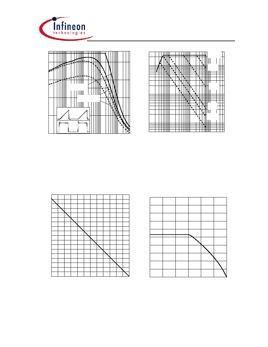
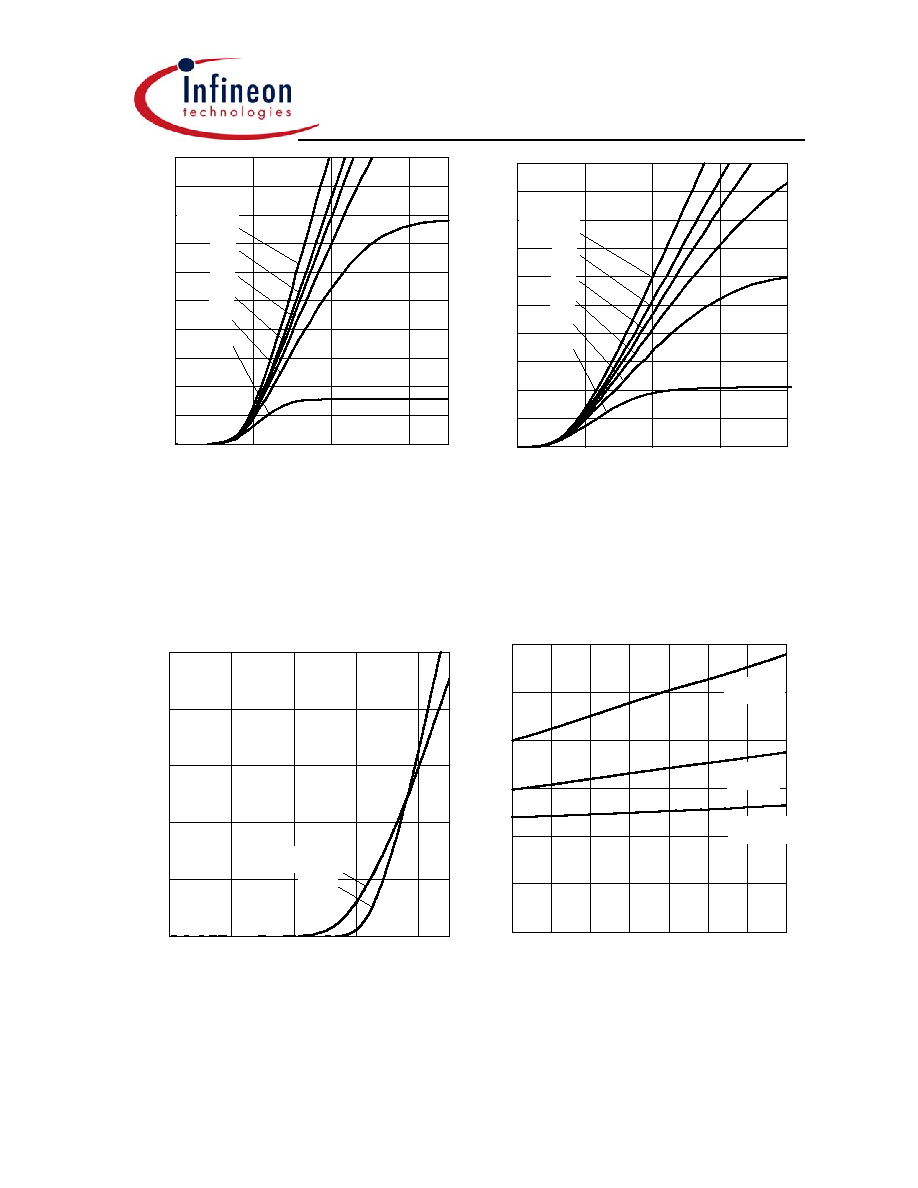
Figure 1. Collector current as a function of
switching frequency
(T
j
175
∞
C, D = 0.5, V
CE
= 400V,
V
GE
= 0/+15V, R
G
= 5
)
Figure 2. Safe operating area
(D = 0, T
C
= 25
∞
C, T
j
175
∞
C;
V
GE
=15V)
P
to
t
,
P
O
W
E
R D
I
SSI
P
A
TI
ON
25∞C
50∞C
75∞C
100∞C 125∞C 150∞C
0W
50W
100W
150W
200W
250W
300W
350W
400W
I
C
,
C
O
LL
E
C
T
O
R CU
RR
E
N
T
25∞C
75∞C
125∞C
0A
30A
60A
90A
120A
T
C
,
CASE TEMPERATURE
T
C
,
CASE TEMPERATURE
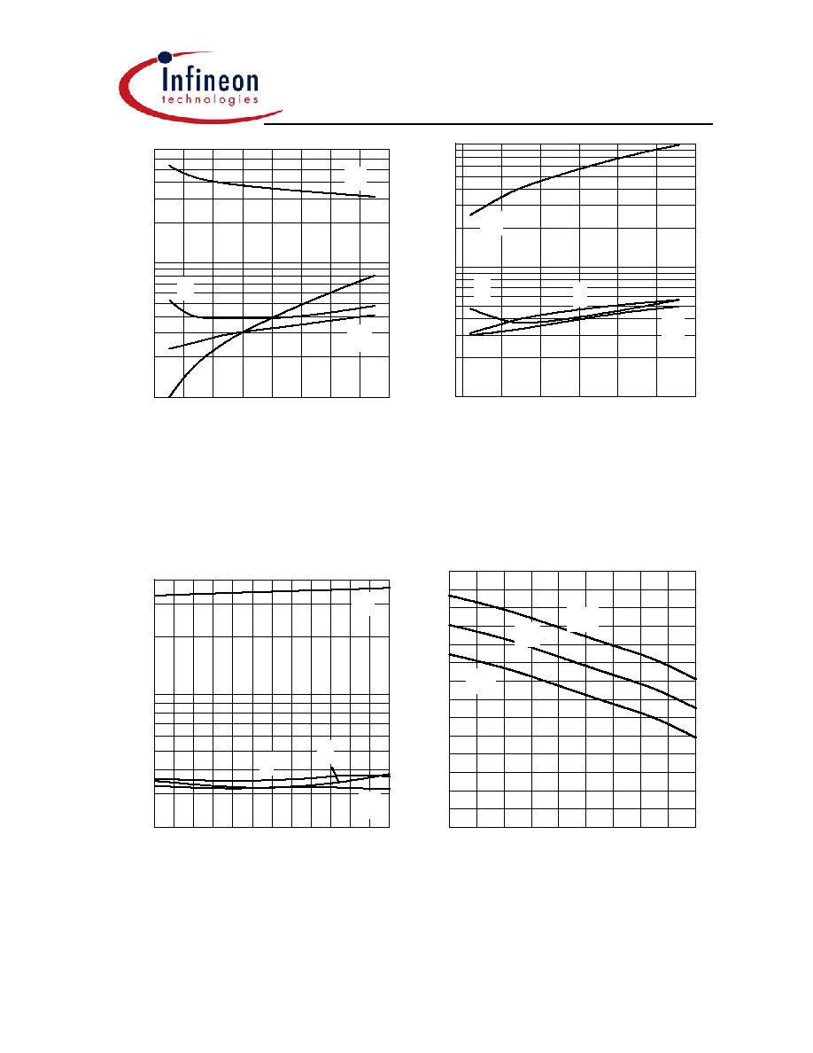
Figure 3. Power dissipation as a function of
case temperature
(T
j
175
∞
C)
Figure 4. DC Collector current as a function
of case temperature
(V
GE
15V, T
j
175
∞
C)
I
c
I
c
IGW75N60T
TrenchStop Series
q
Power Semiconductors
5
Rev. 2.1 Dec-04
I
C
,
COL
L
E
C
T
O
R
CUR
R
E
NT
0V
1V
2V
3V
0A
30A
60A
90A
120A
15V
7V
9V
11V
13V
V
GE
=20V
I
C
,
COL
L
E
C
T
O
R
CUR
R
E
NT
0V
1V
2V
3V
0A
30A
60A
90A
120A
15V
7V
9V
11V
13V
V
GE
=20V
V
CE
,
COLLECTOR
-
EMITTER VOLTAGE
V
CE
,
COLLECTOR
-
EMITTER VOLTAGE
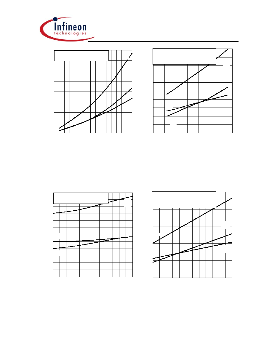
Figure 5. Typical output characteristic
(T
j
= 25∞C)
Figure 6. Typical output characteristic
(T
j
= 175∞C)
I
C
,
COL
L
E
C
T
O
R
CUR
R
E
NT
0V
2V
4 V
6V
8V
0A
20 A
40 A
60 A
80 A
25∞C
T
J
= 17 5∞C
V
CE
(sat),
COL
L
E
CT
OR
-
EM
I
T
T S
A
T
U
R
A
TI
ON
V
O
L
T
AGE
0∞C
50∞C
100∞C
150∞C
0.0V
0.5V
1.0V
1.5V
2.0V
2.5V
I
C
=75A
I
C
=150A
I
C
=37.5A
V
GE
,
GATE-EMITTER
VOLTAGE
T
J
,
JUNCTION TEMPERATURE
Figure 7. Typical transfer characteristic
(V
CE
=20V)
Figure 8. Typical collector-emitter
saturation voltage as a function of
junction temperature
(V
GE
= 15V)
IGW75N60T
TrenchStop Series
q
Power Semiconductors
6
Rev. 2.1 Dec-04
t,
S
W
IT
CHIN
G
TIME
S
0A
40A
80A
120A
10ns
100ns
t
r
t
d(on)
t
f
t
d(off)
t,
S
W
IT
CHIN
G
TIME
S
5
10
15
10ns
100ns
t
r
t
d(on)
t
f
t
d(off)
I
C
,
COLLECTOR CURRENT
R
G
,
GATE RESISTOR
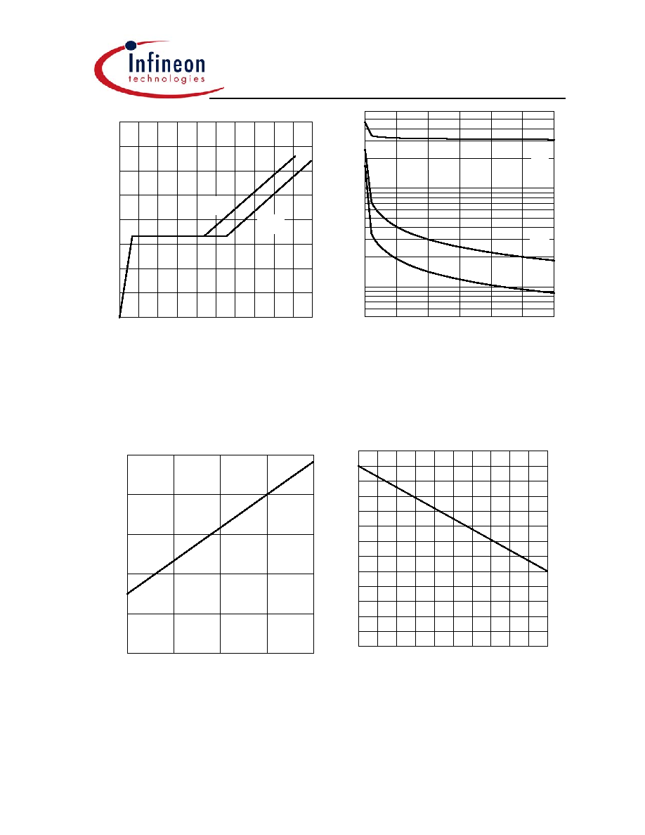
Figure 9. Typical switching times as a
function of collector current
(inductive load, T
J
=175∞C,
V
CE
= 400V, V
GE
= 0/15V, R
G
= 5,
Dynamic test circuit in Figure E)
Figure 10. Typical switching times as a
function of gate resistor
(inductive load, T
J
= 175∞C,
V
CE
= 400V, V
GE
= 0/15V, I
C
= 75A,
Dynamic test circuit in Figure E)
t,
S
W
IT
CHIN
G
TIME
S
25∞C
50∞C
75∞C
100∞C 125∞C 150∞C
100ns
t
r
t
d(on)
t
f
t
d(off)
V
GE
(
t
h
)
,
GAT
E
-
EM
IT
T
TRS
H
O
L
D
VO
L
T
AGE
-50∞C
0∞C
50∞C
100∞C
150∞C
0V
1V
2V
3V
4V
5V
6V
7V
m in.
typ.
m ax.
T
J
,
JUNCTION TEMPERATURE
T
J
,
JUNCTION TEMPERATURE
Figure 11. Typical switching times as a
function of junction temperature
(inductive load, V
CE
= 400V,
V
GE
= 0/15V, I
C
= 75A, R
G
=5,
Dynamic test circuit in Figure E)
Figure 12. Gate-emitter threshold voltage as
a function of junction temperature
(I
C
= 1.2mA)
IGW75N60T
TrenchStop Series
q
Power Semiconductors
7
Rev. 2.1 Dec-04
E
,
SW
I
T
C
H
I
N
G EN
ER
G
Y
L
O
SS
E
S
0A
20A
40A
60A
80A 100A 120A 140A
0.0mJ
4.0mJ
8.0mJ
12.0mJ
E
ts
*
E
off
*) E
on
and E
ts
include losses
due to diode recovery
E
on
*
E
,
SW
I
T
C
H
I
N
G EN
ER
G
Y
L
O
SS
E
S
0
5
10
15
0.0m J
2.0m J
4.0m J
6.0m J
8.0m J
E
ts
*
E
off
*) E
on
and E
ts
include losses
due to diode recovery
E
on
*
I
C
,
COLLECTOR CURRENT
R
G
,
GATE RESISTOR
Figure 13. Typical switching energy losses
as a function of collector current
(inductive load, T
J
= 175∞C,
V
CE
= 400V, V
GE
= 0/15V, R
G
= 5,
Dynamic test circuit in Figure E)
Figure 14. Typical switching energy losses
as a function of gate resistor
(inductive load, T
J
= 175∞C,
V
CE
= 400V, V
GE
= 0/15V, I
C
= 75A,
Dynamic test circuit in Figure E)
E
,
SW
I
T
C
H
I
N
G EN
ER
G
Y
L
O
S
S
E
S
25∞C
50∞C
75∞C
100∞C 125∞C 150∞C
0.0mJ
1.0mJ
2.0mJ
3.0mJ
4.0mJ
5.0mJ
E
ts
*
E
off
*) E
on
and E
ts
include losses
due to diode recovery
E
on
*
E
,
SW
I
T
C
H
I
N
G EN
ER
G
Y
L
O
S
S
E
S
300V 350V 400V 450V 500V 550V
0m J
2m J
4m J
6m J
8m J
E
ts
*
E
on
*
*) E
on
and E
ts
include losses
due to diode recovery
E
off
T
J
,
JUNCTION TEMPERATURE
V
CE
,
COLLECTOR
-
EMITTER VOLTAGE
Figure 15. Typical switching energy losses
as a function of junction
temperature
(inductive load, V
CE
= 400V,
V
GE
= 0/15V, I
C
= 75A, R
G
= 5,
Dynamic test circuit in Figure E)
Figure 16. Typical switching energy losses
as a function of collector emitter
voltage
(inductive load, T
J
= 175∞C,
V
GE
= 0/15V, I
C
= 75A, R
G
= 5,
Dynamic test circuit in Figure E)
IGW75N60T
TrenchStop Series
q
Power Semiconductors
8
Rev. 2.1 Dec-04
V
GE
,
GA
T
E
-
EMI
T
T
E
R V
O
LT
AG
E
0nC
100nC
200nC
300nC
400nC
0V
5V
10V
15V
480V
120V
c,
CAP
A
C
I
T
A
N
C
E
0V
10V
20V
100pF
1nF
C
rss
C
oss
C
iss
Q
GE
,
GATE CHARGE
V
CE
,
COLLECTOR
-
EMITTER VOLTAGE
Figure 17. Typical gate charge
(I
C
=75 A)
Figure 18. Typical capacitance as a function
of collector-emitter voltage
(V
GE
=0V, f = 1 MHz)
I
C
(
sc
)
, sho
r
t
ci
r
c
uit
C
O
LLE
C
T
O
R
CU
RRE
NT
12V
14V
16V
18V
0A
250A
500A
750A
1000A
t
SC
,
SH
ORT
C
I
R
CUI
T
WI
T
H
ST
AND
TI
M
E
10V
11V
12V
13V
14V
0µs
2µs
4µs
6µs
8µs
10µs
12µs
V
GE
,
GATE
-
EMITTETR VOLTAGE
V
GE
,
GATE
-
EMITETR VOLTAGE
Figure 19. Typical short circuit collector
current as a function of gate-
emitter voltage
(V
CE
400V, T
j
150
∞
C)
Figure 20. Short circuit withstand time as a
function of gate-emitter voltage
(V
CE
=600V, start at T
J
=25∞C,
T
Jmax
<150∞C)
IGW75N60T
TrenchStop Series
q
Power Semiconductors
9
Rev. 2.1 Dec-04
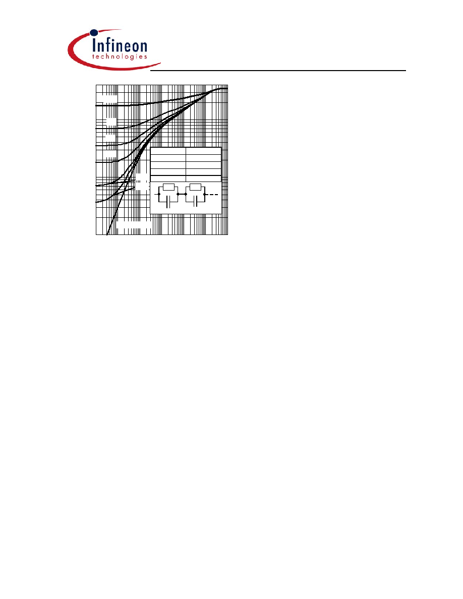
Z
th
JC
,
TRAN
SI
EN
T TH
E
R
M
A
L
R
E
SI
ST
AN
C
E
1µs
10µs 100µs 1ms
10ms 100ms
10
-3
K/W
10
-2
K/W
10
-1
K/W
single pulse
0.01
0.02
0.05
0.1
0.2
D=0.5
t
P
,
PULSE WIDTH
Figure 21. IGBT transient thermal resistance
(D = t
p
/ T)
R
, ( K / W )
,
( s )
0.1968 0.115504
0.0733 0.009340
0.0509 0.000823
0.0290 0.000119
C
1
=
1
/ R
1
R
1
R
2
C
2
=
2
/R
2
IGW75N60T
TrenchStop Series
q
Power Semiconductors
10
Rev. 2.1 Dec-04
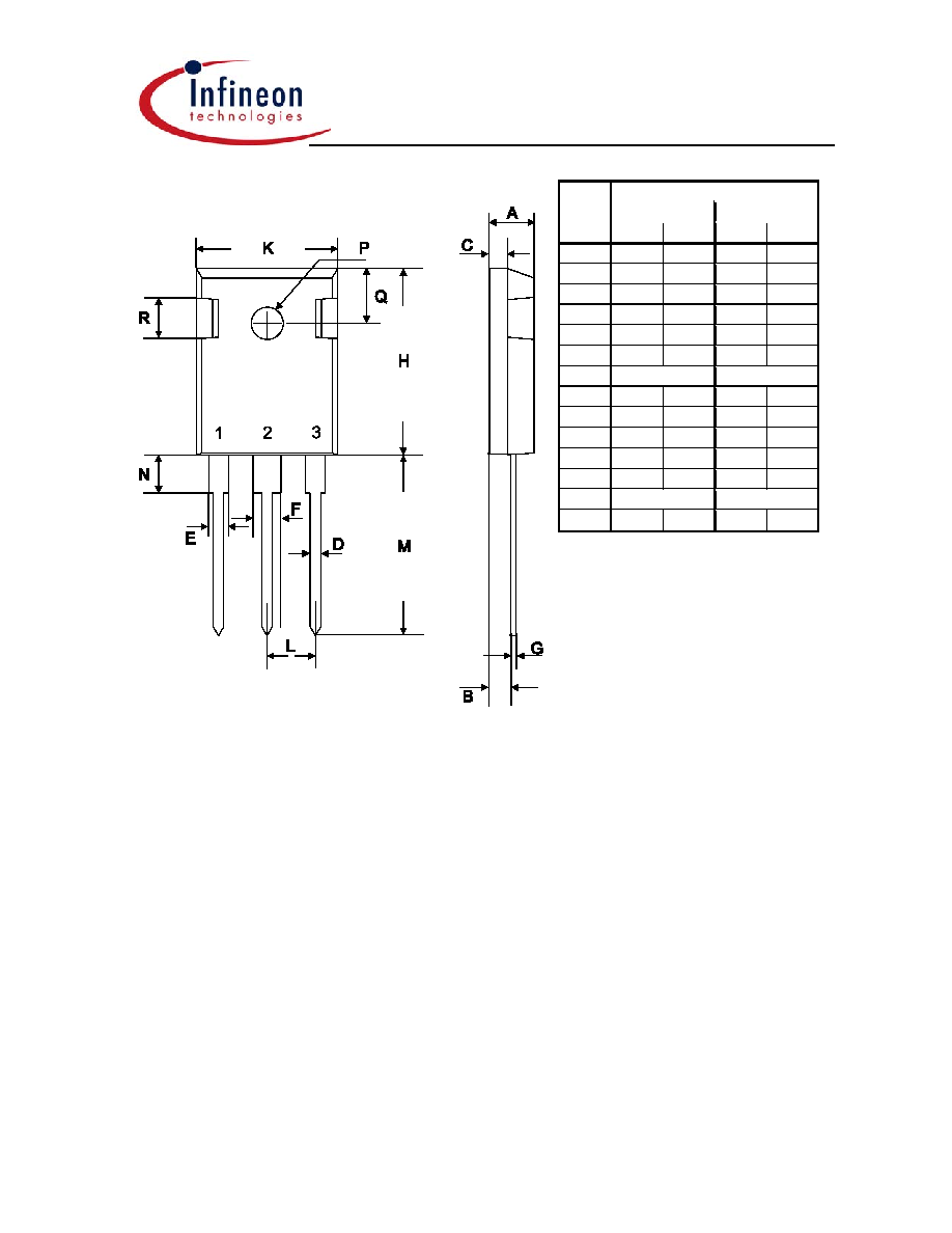
dimensions
symbol
[mm]
[inch]
min
max
min
max
A
4.78
5.28
0.1882 0.2079
B
2.29
2.51
0.0902 0.0988
C
1.78
2.29
0.0701 0.0902
D
1.09
1.32
0.0429 0.0520
E
1.73
2.06
0.0681 0.0811
F
2.67
3.18
0.1051 0.1252
G
0.76 max
0.0299 max
H
20.80
21.16
0.8189 0.8331
K
15.65
16.15
0.6161 0.6358
L
5.21
5.72
0.2051 0.2252
M
19.81
20.68
0.7799 0.8142
N
3.560
4.930
0.1402 0.1941
P
3.61
0.1421
Q
6.12
6.22
0.2409 0.2449
TO-247AC
IGW75N60T
TrenchStop Series
q
Power Semiconductors
11
Rev. 2.1 Dec-04
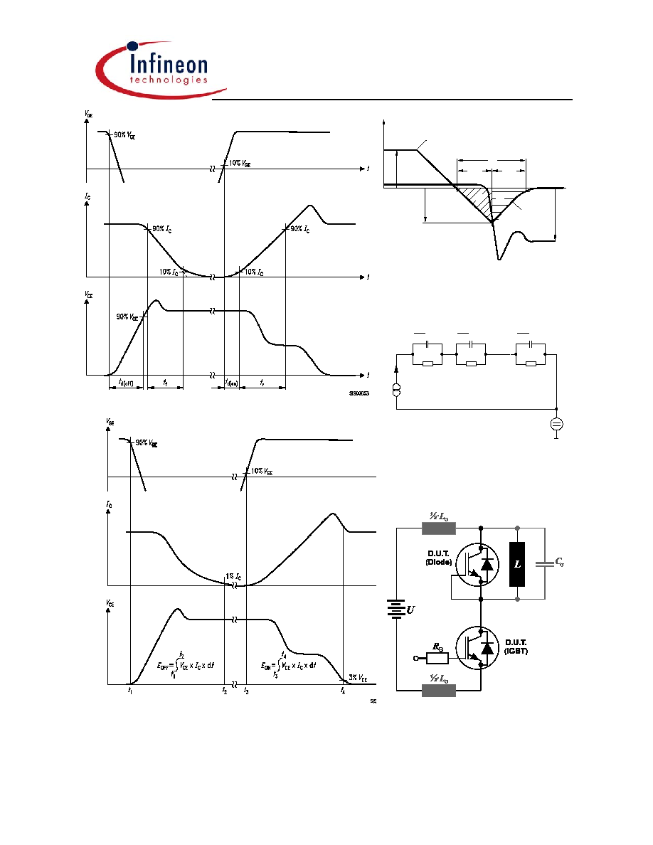
Figure A. Definition of switching times
Figure B. Definition of switching losses
I
r r m
90% I
r r m
10% I
r r m
di /dt
F
t
r r
I
F
i,v
t
Q
S
Q
F
t
S
t
F
V
R
di /dt
r r
Q =Q
Q
r r
S
F
+
t =t
t
r r
S
F
+
Figure C. Definition of diodes
switching characteristics
p(t)
1
2
n
T (t)
j
1
1
2
2
n
n
T
C
r
r
r
r
r
r
Figure D. Thermal equivalent
circuit
Figure E. Dynamic test circuit

IGW75N60T
TrenchStop Series
q
Power Semiconductors
12
Rev. 2.1 Dec-04
Published by
Infineon Technologies AG,
Bereich Kommunikation
St.-Martin-Strasse 53,
D-81541 M¸nchen
© Infineon Technologies AG 2004
All Rights Reserved.
Attention please!
The information herein is given to describe certain components and shall not be considered as warranted characteristics.
Terms of delivery and rights to technical change reserved.
We hereby disclaim any and all warranties, including but not limited to warranties of non-infringement, regarding circuits,
descriptions and charts stated herein.
Infineon Technologies is an approved CECC manufacturer.
Information
For further information on technology, delivery terms and conditions and prices please contact your nearest Infineon
Technologies Office in Germany or our Infineon Technologies Representatives worldwide (see address list).
Warnings
Due to technical requirements components may contain dangerous substances. For information on the types in question
please contact your nearest Infineon Technologies Office.
Infineon Technologies Components may only be used in life-support devices or systems with the express written
approval of Infineon Technologies, if a failure of such components can reasonably be expected to cause the failure of
that life-support device or system, or to affect the safety or effectiveness of that device or system. Life support devices or
systems are intended to be implanted in the human body, or to support and/or maintain and sustain and/or protect
human life. If they fail, it is reasonable to assume that the health of the user or other persons may be endangered.