Genesys
2001-04-05
Page 1
IPP15N03L
IPB15N03L
Preliminary data
OptiMOS
=
=
=
=
Buck converter series
Product Summary
V
DS
30
V
R
DS(on)
max. SMD version
12.6
m
I
D
42
A
Feature
N-Channel
Logic Level
Low on-resistance R
DS(on)
Excellent Gate Charge x R
DS(on)
product (FOM)
Superior thermal resistance
175°C operating temperature
dv/dt rated
Ideal for fast switching buck converters
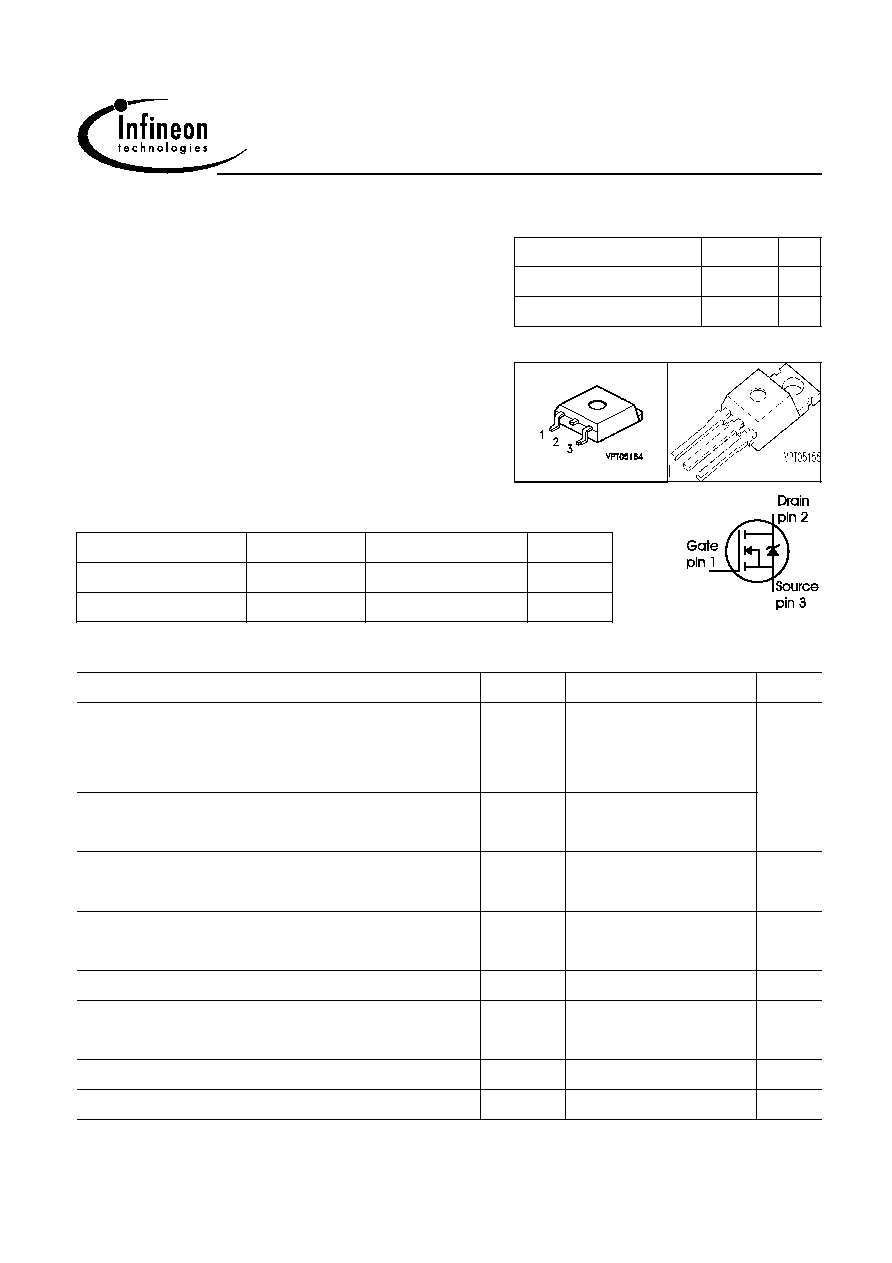
P-TO263-3-2
P-TO220-3-1
Marking
15N03L
15N03L
Type
Package
Ordering Code
IPP15N03L
P-TO220-3-1 Q67042-S4039
IPB15N03L
P-TO263-3-2 Q67040-S4344
Maximum Ratings,at T
j
= 25 °C, unless otherwise specified
Parameter
Symbol
Value
Unit
Continuous drain current
T
C
=25°C
T
C
=100°C
I
D
42
35
A
Pulsed drain current
T
C
=25°C
I
D puls
168
Avalanche energy, single pulse
I
D
=20A, V
DD
=25V, R
GS
=25
E
AS
20
mJ
Reverse diode dv/dt
I
S
=42A, V
DS
=-V, di/dt=200A/µs, T
jmax
=175°C
dv/dt
6
kV/µs
Gate source voltage
V
GS
±20
V
Power dissipation
T
C
=25°C
P
tot
64
W
Operating and storage temperature
T
j ,
T
stg
-55... +175
°C
IEC climatic category; DIN IEC 68-1
55/175/56
2001-04-05
Page 2
IPP15N03L
IPB15N03L
Preliminary data
Thermal Characteristics
Parameter
Symbol
Values
Unit
min.
typ.
max.
Characteristics
Thermal resistance, junction - case
R
thJC
-
-
2.3
K/W
SMD version, device on PCB:
@ min. footprint
@ 6 cm
2
cooling area
1)
R
thJA
-
-
-
-
62
40
Electrical Characteristics, at T
j
= 25 °C, unless otherwise specified
Parameter
Symbol
Values
Unit
min.
typ.
max.
Static Characteristics
Drain-source breakdown voltage
V
GS
=0V, I
D
=1mA
V
(BR)DSS
30
-
-
V
Gate threshold voltage, V
GS
= V
DS
I
D
=40µA
V
GS(th)
1.2
1.6
2
Zero gate voltage drain current
V
DS
=30V, V
GS
=0V, T
j
=25°C
V
DS
=30V, V
GS
=0V, T
j
=125°C
I
DSS
-
-
0.01
10
1
100
µA
Gate-source leakage current
V
GS
=20V, V
DS
=0V
I
GSS
-
1
100
nA
Drain-source on-state resistance
V
GS
=4.5V, I
D
=21A
V
GS
=4.5V, I
D
=21A, SMD version
R
DS(on)
-
-
15
14.7
19.9
19.6
m
Drain-source on-state resistance
V
GS
=10V, I
D
=21A
V
GS
=10V, I
D
=21A, SMD version
R
DS(on)
-
-
9.5
9.2
12.9
12.6
1Device on 40mm*40mm*1.5mm epoxy PCB FR4 with 6cm² (one layer, 70 µm thick) copper area for drain
connection. PCB is vertical without blown air.
2001-04-05
Page 3
IPP15N03L
IPB15N03L
Preliminary data
Electrical Characteristics, at T
j
= 25 °C, unless otherwise specified
Parameter
Symbol
Conditions
Values
Unit
min.
typ.
max.
Dynamic Characteristics
Transconductance
g
fs
V
DS
2*I
D
*R
DS(on)max
,
I
D
=35A
21
42
-
S
Input capacitance
C
iss
V
GS
=0V, V
DS
=25V,
f
=1MHz
-
895
1120 pF
Output capacitance
C
oss
-
365
455
Reverse transfer capacitance
C
rss
-
82
102
Gate resistance
R
G
-
1
-
Turn-on delay time
t
d(on)
V
DD
=15V, V
GS
=10V,
I
D
=21A, R
G
=7.8
-
6.5
9.8
ns
Rise time
t
r
-
58
87
Turn-off delay time
t
d(off)
-
24
36
Fall time
t
f
-
14.5
21.8
Gate Charge Characteristics
Gate to source charge
Q
gs
V
DD
=15V, I
D
=21A
-
3
3.8
nC
Gate to drain charge
Q
gd
-
7.4
9.3
Gate charge total
Q
g
V
DD
=15V, I
D
=21A,
V
GS
=0 to 5V
-
12.7
15.9
Output charge
Q
oss
V
DS
=15V, I
D
=21A,
V
GS
=0V
-
12.2
15.3
Gate plateau voltage
V
(plateau) V
DD
=15V, I
D
=21A
-
3.5
-
V
Reverse Diode
Inverse diode continuous
forward current
I
S
T
C
=25°C
-
-
42
A
Inverse diode direct current,
pulsed
I
SM
-
-
168
Inverse diode forward voltage V
SD
V
GS
=0V, I
F
=42A
-
0.95
1.25 V
Reverse recovery time
t
rr
V
R
=-V, I
F=
l
S
,
di
F
/dt
=100A/µs
-
22
33
ns
Reverse recovery charge
Q
rr
-
11.5
18
nC
2001-04-05
Page 4
IPP15N03L
IPB15N03L
Preliminary data
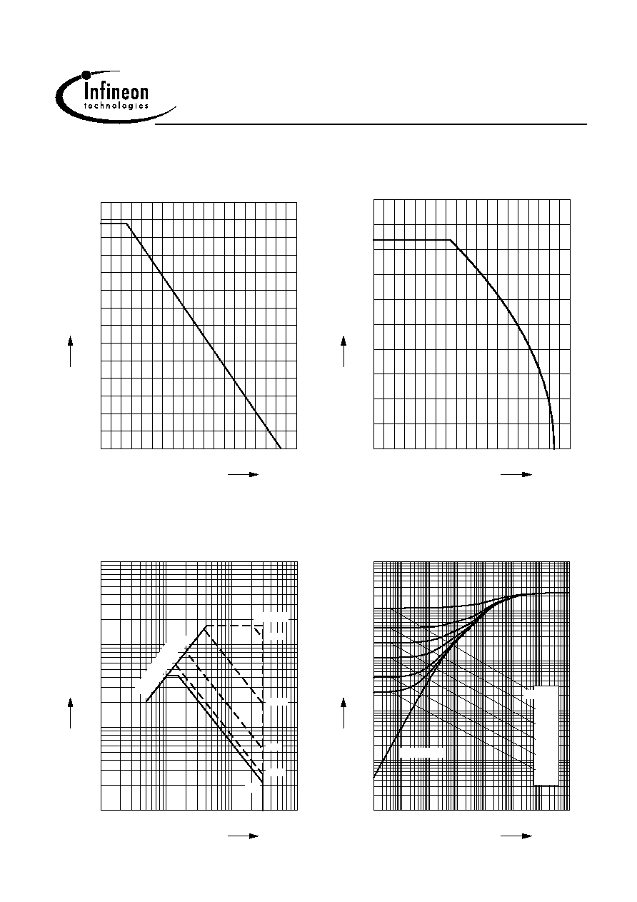
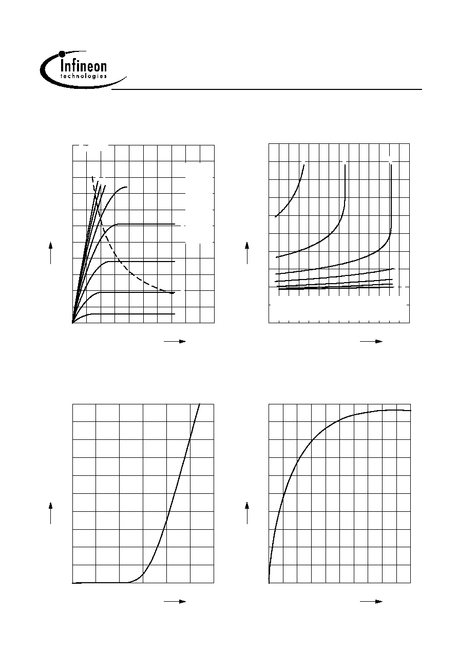
1 Power dissipation
P
tot
= f (T
C
)
0
20
40
60
80 100 120 140 160
°C
190
T
C
0
5
10
15
20
25
30
35
40
45
50
55
60
W
70
IPP15N03L
P
tot
2 Drain current
I
D
= f (T
C
)
parameter: V
GS
10 V
0
20
40
60
80 100 120 140 160
°C
190
T
C
0
5
10
15
20
25
30
35
40
A
50
IPP15N03L
I
D
3 Safe operating area
I
D
= f ( V
DS
)
parameter : D = 0 , T
C
= 25 °C
10
-1
10
0
10
1
10
2
V
V
DS
0
10
1
10
2
10
3
10
A
IPP15N03L
I
D
R
D
S(
on
)
=
V
D
S
/
I
D
DC
10 ms
1 ms
100 µs
10 µs
tp = 6.8µs
4 Transient thermal impedance
Z
thJC
= f (t
p
)
parameter : D = t
p
/T
10
-7
10
-6
10
-5
10
-4
10
-3
10
-2
10
0
s
t
p
-4
10
-3
10
-2
10
-1
10
0
10
1
10
K/W
IPP15N03L
Z
thJC
single pulse
0.01
0.02
0.05
0.10
0.20
D = 0.50
2001-04-05
Page 5
IPP15N03L
IPB15N03L
Preliminary data
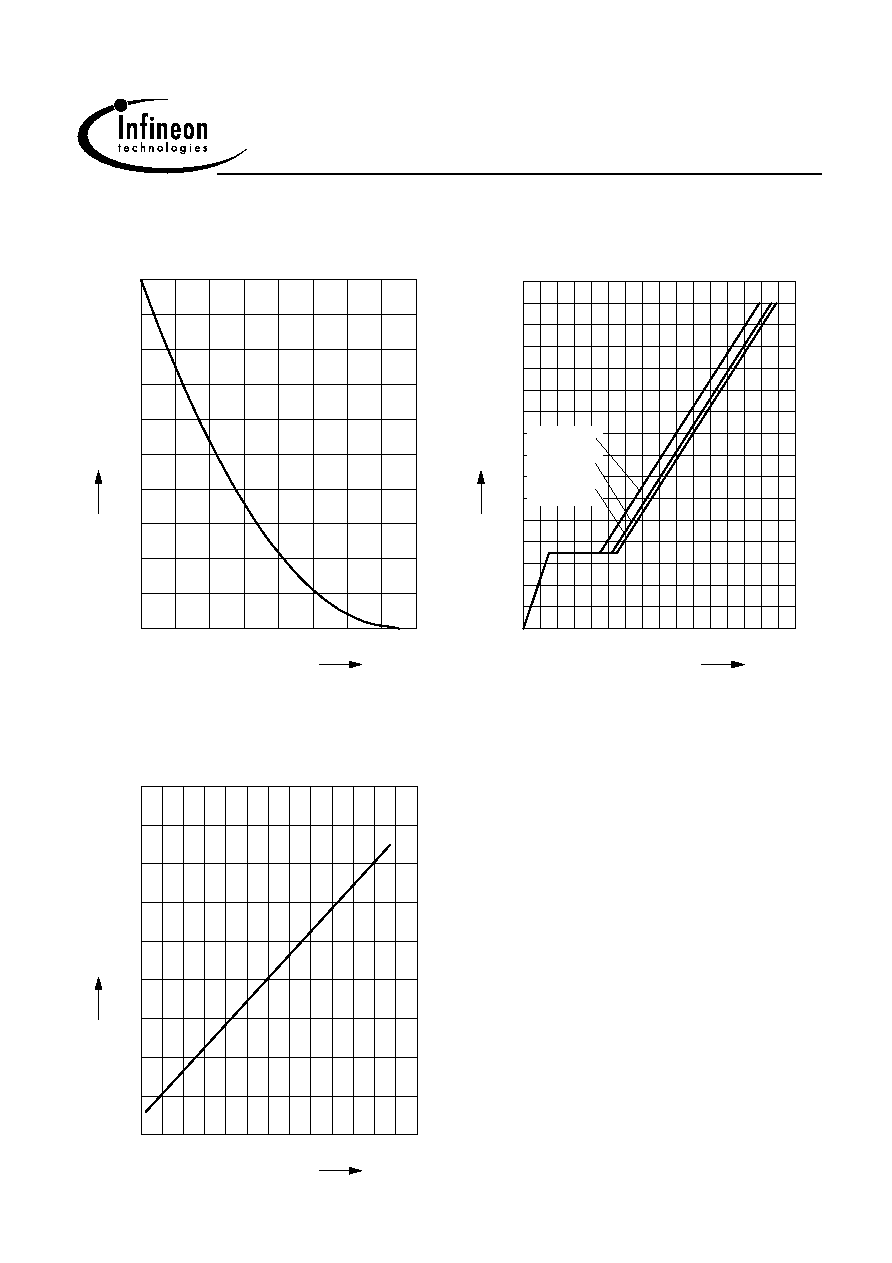
5 Typ. output characteristic
I
D
= f (V
DS
); T
j
=25°C
parameter: t
p
= 80 µs
0
0.5
1
1.5
2
2.5
3
3.5
4
V
5
V
DS
0
10
20
30
40
50
60
70
80
90
A
110
IPP15N03L
I
D
VGS [V]
a
a
3.0
b
b
3.5
c
c
4.0
d
d
4.5
e
e
5.0
f
f
5.5
g
g
6.0
h
P
tot
= 64W
h
10.0
6 Typ. drain-source on resistance
R
DS(on)
= f (I
D
)
parameter: V
GS
0
10
20
30
40
50
A
70
I
D
0
0.005
0.01
0.015
0.02
0.025
0.03
0.035
0.04
0.05
IPP15N03L
R
DS(on)
V
GS
[V] =
b
b
3.5
c
c
4.0
d
d
4.5
e
e
5.0
f
f
5.5
g
g
6.0
h
h
10.0
7 Typ. transfer characteristics
I
D
= f ( V
GS
); V
DS
2 x I
D
x R
DS(on)max
parameter: t
p
= 80 µs
0
1
2
3
4
V
6
V
GS
0
10
20
30
40
50
60
70
80
A
100
I
D
8 Typ. forward transconductance
g
fs
= f(I
D
); T
j
=25°C
parameter: g
fs
0
10
20
30
40
50
60
70
80
A
100
I
D
0
5
10
15
20
25
30
35
40
S
50
g
fs

2001-04-05
Page 6
IPP15N03L
IPB15N03L
Preliminary data
9 Drain-source on-state resistance
R
DS(on)
= f (T
j
)
parameter : I
D
= 21 A, V
GS
= 10 V
-60
-20
20
60
100
140 °C
200
T
j
0
2
4
6
8
10
12
14
16
18
20
22
24
30
IPP15N03L
R
DS(on)
typ
98%
10 Gate threshold voltage
V
GS(th)
= f (Tj)
parameter: V
GS
= V
DS
, I
D
= 40 µA
-60
-20
20
60
100
°C
160
T
j
0
0.5
1
1.5
V
2.5
V
GS(th)
min.
typ.
max.
11 Typ. capacitances
C = f (V
DS
)
parameter: V
GS
=0V, f=1 MHz
0
5
10
15
20
V
30
V
DS
1
10
2
10
3
10
4
10
V
pF
C
iss
C
oss
C
rss
12 Forward character. of reverse diode
I
F
= f (V
SD
)
parameter: Tj , t
p
= 80 µs
0
0.4
0.8
1.2
1.6
2
2.4
V
3
V
SD
0
10
1
10
2
10
3
10
A
IPP15N03L
I
F
T
j
= 25 °C typ
T
j
= 25 °C (98%)
T
j
= 175 °C typ
T
j
= 175 °C (98%)
2001-04-05
Page 7
IPP15N03L
IPB15N03L
Preliminary data
13 Typ. avalanche energy
E
AS
= f (T
j
)
par.: I
D
= 20 A, V
DD
= 25 V, R
GS
= 25
25
45
65
85
105
125
145
°C
185
T
j
0
2
4
6
8
10
12
14
16
mJ
20
E
AS
14 Typ. gate charge
V
GS
= f (Q
Gate
)
parameter: I
D
= 21 A pulsed
0
4
8
12
16
20
24
nC
32
Q
Gate
0
2
4
6
8
10
12
V
16
IPP15N03L
V
GS
0.2 V
DS max
0.5 V
DS max
0.8 V
DS max
15 Drain-source breakdown voltage
V
(BR)DSS
= f (T
j
)
parameter: I
D
=10 mA
-60
-20
20
60
100
140
°C
200
T
j
27
28
29
30
31
32
33
34
V
36
IPP15N03L
V
(BR)DSS

2001-04-05
Page 8
IPP15N03L
IPB15N03L
Preliminary data
Published by
Infineon Technologies AG,
Bereichs Kommunikation
St.-Martin-Strasse 53,
D-81541 München
© Infineon Technologies AG 1999
All Rights Reserved.
Attention please!
The information herein is given to describe certain components and shall not be considered as warranted
characteristics.
Terms of delivery and rights to technical change reserved.
We hereby disclaim any and all warranties, including but not limited to warranties of non-infringement,
regarding circuits, descriptions and charts stated herein.
Infineon Technologies is an approved CECC manufacturer.
Information
For further information on technology, delivery terms and conditions and prices please contact your nearest
Infineon Technologies Office in Germany or our Infineon Technologies Reprensatives worldwide (see address list).
Warnings
Due to technical requirements components may contain dangerous substances.
For information on the types in question please contact your nearest Infineon Technologies Office.
Infineon Technologies Components may only be used in life-support devices or systems with the express
written approval of Infineon Technologies, if a failure of such components can reasonably be expected to
cause the failure of that life-support device or system, or to affect the safety or effectiveness of that device
or system Life support devices or systems are intended to be implanted in the human body, or to support
and/or maintain and sustain and/or protect human life. If they fail, it is reasonable to assume that the health
of the user or other persons may be endangered.