LB 5413, LV 5413, LT 5413
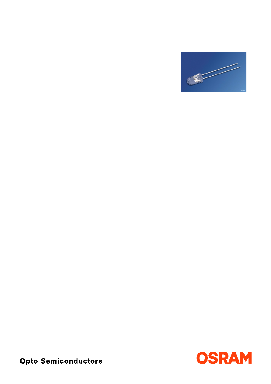
Hyper 5 mm (T1 æ) LED, Non Diffused
Hyper-Bright LED
Vorl‰ufige Daten / Preliminary Data
2001-03-01
1
Besondere Merkmale
∑ Geh‰usetyp: nicht eingef‰rbtes, klares 5 mm
(T1 æ) Geh‰use
∑ Besonderheit des Bauteils: enge
Abstrahlcharakteristik f¸r groþe Lichtst‰rken
∑ Wellenl‰nge: 470 nm (blau), 505 nm (verde),
528 nm (true green)
∑ Abstrahlwinkel: engwinklig (15∞)
∑ Technologie: InGaN
∑ optischer Wirkungsgrad: 2 lm/W (blau),
6 lm/W (verde), 8 lm/W (true green)
∑ Gruppierungsparameter: Lichtst‰rke
∑ Lˆtmethode: Wellenlˆten (TTW)
∑ Verpackung: Sch¸ttgut, gegurtet lieferbar
∑ ESD-Festigkeit: ESD-sicher bis 2 kV nach
EOS/ESD-5.1-1993
Anwendungen
∑ Ampelanwendungen
∑ Hinterleuchtung (LCD, Schalter, Tasten,
Displays, Werbebeleuchtung,
Allgemeinbeleuchtung)
∑ Innenbeleuchtung im Automobilbereich
(z.B. Tastenbeleuchtung, u. ‰.)
∑ Ersatz von Kleinst-Gl¸hlampen
Features
∑ package: colorless, clear 5 mm (T1 æ)
package
∑ feature of the device: narrow viewing angle for
more brightness
∑ wavelength: 470 nm (blue), 505 nm (verde),
528 nm (true green)
∑ viewing angle: narrow (15∞)
∑ technology: InGaN
∑ optical efficiency: 2 lm/W (blue),
6 lm/W (verde), 8 lm/W (true green)
∑ grouping parameter: luminous intensity
∑ soldering methods: TTW soldering
∑ packing: bulk, available taped on reel
∑ ESD-withstand voltage: up to 2 kV acc. to
EOS/ESD-5.1-1993
Applications
∑ traffic lights
∑ backlighting (LCD, switches, keys, displays,
illuminated advertising, general lighting)
∑ interior automotive lighting (e.g. key
backlighting, etc.)
∑ substitution of micro incandescent lamps
2001-03-01
2
LB 5413, LV 5413, LT 5413
Anm.:
- gesamter Farbbereich, Lieferung in Einzelgruppen (siehe Seite 5)
Die Standardlieferform von Serientypen beinhaltet eine untere bzw. eine obere Familiengruppe oder
mindestens zwei Einzelgruppen.
In einer Verpackungseinheit / Gurt ist immer nur eine Helligkeitsgruppe enthalten.
Die technologiebedingte Helligkeits-Streuung der heutigen LED-Herstellprozesse ¸ber einen l‰ngeren
Fertigungszeitraum (Halbleitermaterial - Chipherstellung - Montageprozesss) erlaubt keine Zusage einer
einzelnen Helligkeitsgruppe. Daher m¸ssen mindestens zwei Helligkeitsgruppen vorgesehen werden!
Note:
- Total color tolerance range, delivery in single groups (please see page 5)
The standard shipping format for serial types includes a lower or upper family group or at least two individual
groups.
No packing unit / tape ever contains more than one luminous intensity group.
Luminosity variations caused by the technology used in current LED manufacturing processes over a
protracted manufacturing period (semiconductor material - chip fabrication - assembly process) mean that it is
not possible to assign LEDs to a single luminous intensity group. For this reason at least two luminous intensity
groups must be provided!
Typ
Type
Emissions-
farbe
Color of
Emission
Geh‰usefarbe
Color of
Package
Lichtst‰rke
Luminous
Intensity
I
F
= 20 mA
I
V
(mcd)
Lichtstrom
Luminous
Flux
I
F
= 20 mA
V
(mlm)
Bestellnummer
Ordering Code
LB 5413-TV
LB 5413-VBW
LB 5413-T
LB 5413-U
LB 5413-V
LB 5413-AW
LB 5413-BW
blue
colorless clear
280 ... 1120
710 ... 2800
280 ... 450
450 ... 710
710 ... 1120
1120 ... 1800
1800 ... 2800
120 (typ.)
300 (typ.)
60 (typ.)
100 (typ.)
150 (typ.)
240 (typ.)
380 (typ.)
Q62703-Q5930
Q62703-Q5931
LV 5413-VBW
LV 5413-BWDW
LV 5413-V
LV 5413-AW
LV 5413-BW
LV 5413-CW
LV 5413-DW
verde
colorless clear
710 ... 2800
1800 ... 7100
710 ... 1120
1120 ... 1800
1800 ... 2800
2800 ... 4500
4500 ... 7100
470 (typ.)
1200 (typ.)
230 (typ.)
370 (typ.)
590 (typ.)
900 (typ.)
1400 (typ.)
Q62703-Q5932
Q62703-Q5933
LT 5413-VBW
LT 5413-BWDW
LT 5413-V
LT 5413-AW
LT 5413-BW
LT 5413-CW
LT 5413-DW
true green
colorless clear
710 ... 2800
1800 ... 7100
710 ... 1120
1120 ... 1800
1800 ... 2800
2800 ... 4500
4500 ... 7100
470 (typ.)
1200 (typ.)
230 (typ.)
370 (typ.)
590 (typ.)
900 (typ.)
1400 (typ.)
Q62703-Q5934
Q62703-Q5935
LB 5413, LV 5413, LT 5413
2001-03-01
3
Grenzwerte
Maximum Ratings
Bezeichnung
Parameter
Symbol
Symbol
Wert
Value
Einheit
Unit
LB
LV, LT
Betriebstemperatur
Operating temperature range
T
op
≠ 55 ... + 100
∞C
Lagertemperatur
Storage temperature range
T
stg
≠ 55 ... + 100
∞C
Sperrschichttemperatur
Junction temperature
T
j
+ 100
∞C
Durchlassstrom
Forward current
I
F
20
mA
Stoþstrom
Surge current
t
10
µ
s,
D
= 0.005
I
FM
200
250
mA
Sperrspannung
Reverse voltage
V
R
5
V
Leistungsaufnahme
Power consumption
T
A
25 ∞C
P
tot
85
mW
W‰rmewiderstand
Thermal resistance
Sperrschicht/Umgebung
Junction/ambient
Sperrschicht/Lˆtpad
Junction/solder point
Montage auf PC-Board FR 4 (Padgrˆþe
16 mm
2
)
mounted on PC board FR 4 (pad size
16 mm
2
)
Minimale Beinchenl‰nge
Minimum lead length
R
th JA
R
th JS
400
180
K/W
K/W
2001-03-01
4
LB 5413, LV 5413, LT 5413
Kennwerte (
T
A
= 25 ∞C)
Characteristics
Bezeichnung
Parameter
Symbol
Symbol
Werte
Values
Einheit
Unit
LB
LV
LT
Wellenl‰nge des emittierten Lichtes
(typ.)
Wavelength at peak emission
I
F
= 20 mA
peak
465
503
523
nm
Dominantwellenl‰nge
1)
(typ.)
Dominant wavelength
I
F
= 20 mA
dom
470
± 6
505
± 7
528
± 9
nm
Spektrale Bandbreite bei 50 %
I
rel max
(typ.)
Spectral bandwidth at 50 %
I
rel max
I
F
= 20 mA
25
30
33
nm
Abstrahlwinkel bei 50 %
I
V
(Vollwinkel)
(typ.)
Viewing angle at 50 %
I
V
2
15
15
15
Grad
deg.
Durchlassspannung
2)
(typ.)
Forward voltage
(max.)
I
F
= 20 mA
V
F
V
F
3.5
4.1
3.3
4.1
3.3
4.1
V
V
Sperrstrom
(typ.)
Reverse current
(max.)
V
R
= 5 V
I
R
I
R
0.01
10
0.01
10
0.01
10
µ
A
µ
A
Temperaturkoeffizient von
peak
(typ.)
Temperature coefficient of
peak
I
F
= 20 mA; ≠10∞C
T
100∞C
TC
peak
0.04
0.03
0.04
nm/K
Temperaturkoeffizient von
dom
(typ.)
Temperature coefficient of
dom
I
F
= 20 mA; ≠10∞C
T
100∞C
TC
dom
0.02
0.02
0.03
nm/K
Temperaturkoeffizient von
V
F
(typ.)
Temperature coefficient of
V
F
I
F
= 20 mA; ≠10∞C
T
100∞C
TC
V
≠ 2.9
≠ 3.2
≠ 3.6
mV/K
Optischer Wirkungsgrad
(typ.)
Optical efficiency
I
F
= 20 mA
opt
2
6
8
lm/W
1)
Wellenl‰ngengruppen werden mit einer Stromeinpr‰gedauer von 25 ms und einer Genauigkeit von ±1 nm ermittelt.
Wavelength groups are tested at a current pulse duration of 25 ms and a tolerance of ±1 nm.
2)
Spannungswerte werden mit einer Stromeinpr‰gedauer von 1 ms und einer Genauigkeit von ±0.1 V ermittelt.
Voltages are tested at a current pulse duration of 1 ms and a tolerance of ±0.1 V.
LB 5413, LV 5413, LT 5413
2001-03-01
5
1)
Wellenl‰ngengruppen / Wavelength groups
Helligkeitswerte werden mit einer Stromeinpr‰gedauer von 25 ms und einer Genauigkeit von
±
11% ermittelt.
Luminous intensity is tested at a current pulse duration of 25 ms and a tolerance of
±
11%.
Gruppe
Group
blue
verde
true green
Einheit
Unit
min.
max. min.
max. min.
max.
3
464
468
498
503
519
525
nm
4
468
472
503
507
525
531
nm
5
472
476
507
512
531
537
nm
Helligkeits-Gruppierungsschema
Luminous Intensity Groups
Lichtgruppe
Luminous Intensity Group
Lichtst‰rke
Luminous Intensity
I
V
(mcd)
Lichtstrom
Luminous Flux
V
(mlm)
T
U
V
AW
BW
CW
DW
280 ... 450
450 ... 710
710 ... 1120
1120 ... 1800
1800 ... 2800
2800 ... 4500
4500 ... 7100
60 (typ.)
100 (typ.)
150 (typ.)
240 (typ.)
380 (typ.)
900 (typ.)
1400 (typ.)
2001-03-01
6
LB 5413, LV 5413, LT 5413
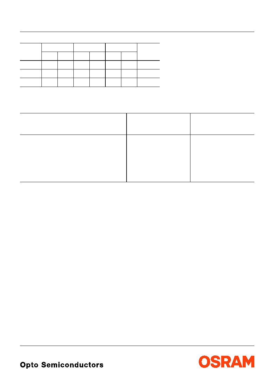
Relative spektrale Emission
I
rel
=
f
(
),
T
A
= 25 ∞C,
I
F
= 20 mA
Relative Spectral Emission
V(
) = spektrale Augenempfindlichkeit
Standard eye response curve
Abstrahlcharakteristik
I
rel
=
f
(
)
Radiation Characteristic
0
400
true green
550
450
500
600
650
nm
700
OHL00492
I
20
40
60
80
%
100
rel
verde
blue
V
OHL00493
0∞
20∞
40∞
60∞
80∞
100∞
120∞
0.4
0.6
0.8
1.0
00∞
90∞
80∞
70∞
60∞
50∞
0∞
10∞
20∞
30∞
40∞
0
0.2
0.4
0.6
0.8
1.0
LB 5413, LV 5413, LT 5413
2001-03-01
7
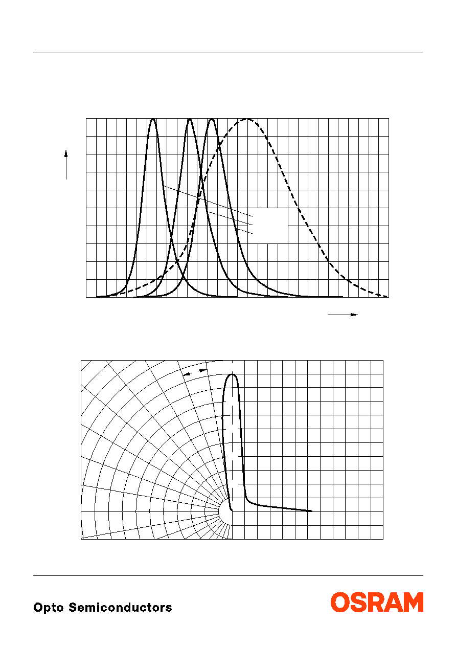
Durchlassstrom
I
F
=
f
(
V
F
)
Forward Current
T
A
= 25 ∞C
Maximal zul‰ssiger Durchlassstrom
I
F
=
f
(
T
)
Max. Permissible Forward Current
Relative Lichtst‰rke
I
V
/
I
V(20 mA)
=
f
(
I
F
)
Relative Luminous Intensity
T
A
= 25 ∞C
Maximal zul‰ssiger Durchlassstrom
I
F
=
f
(
T
)
Max. Permissible Forward Current
OHL00495
10
-1
2.5
3
3.5
4
4.5 V 5
0
10
1
10
10
2
5
5
mA
5
2
true green
verde,
blue
I
F
V
F
OHL01398
0
0
∞C
mA
F
I
T
5
10
15
20
25
30
20
40
60
80
100
temp. ambient
A
T
OHL00494
10
-2
-1
10
0
10
10
1
5
5
-1
10
10
0
10
1
10
mA
2
I
F
V
V (20 mA)
I
I
OHL01399
0
0
20
40
60
80 ∞C 100
T
I
F
5
10
15
20
25
30
mA
temp. solder point
S
T
LB 5413, LV 5413, LT 5413
2001-03-01
8
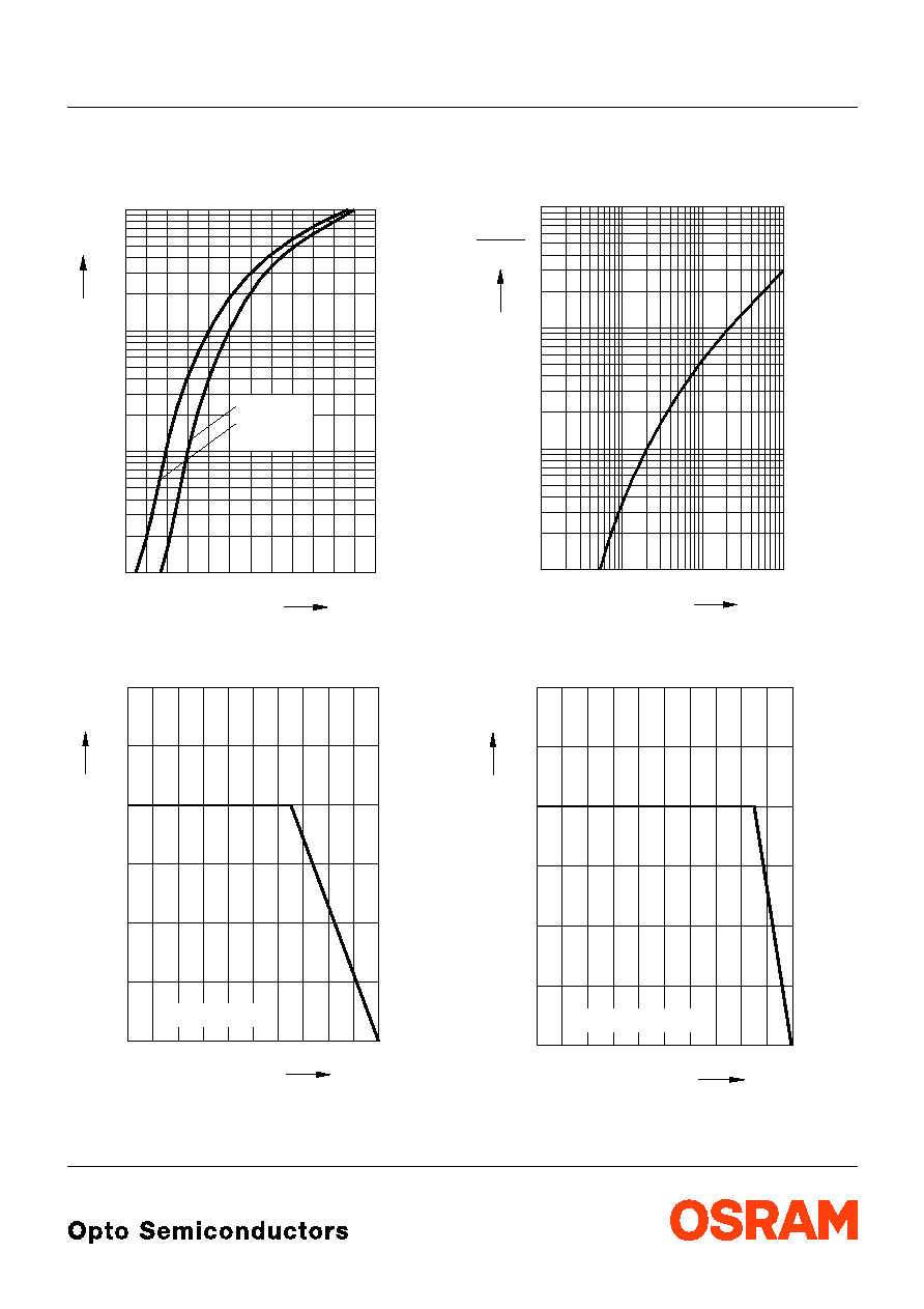
Relative Lichtst‰rke
I
V
/
I
V(25 ∞C)
=
f
(
T
A
)
Relative Luminous Intensity
I
F
= 20 mA
Dominante Wellenl‰nge
dom
=
f
(
I
F
)
Dominant Wavelength
LV
, T
A
= 25 ∞C
Dominante Wellenl‰nge
dom
=
f
(
I
F
)
Dominant Wavelength
LB
, T
A
= 25 ∞C
Dominante Wellenl‰nge
dom
=
f
(
I
F
)
Dominant Wavelength
LT
, T
A
= 25 ∞C
OHL00870
0
-10
V
V (25 ∞C)
I
I
∞C
V
A
T
10
30
50
70
100
0.2
0.4
0.6
0.8
1.2
I
OHL00503
502
dom
0
F
10
20
30
40 mA 50
503
504
505
506
507
508
509
510
511
nm
verde
I
OHL00500
469.0
dom
0
F
10
20
30
40 mA 50
469.5
470.0
470.5
471.0
471.5
472.5
nm
blue
I
OHL00882
521
dom
0
F
10
20
30
40 mA 50
523
525
527
529
531
533
535
537
nm
541
true green
539
LB 5413, LV 5413, LT 5413
2001-03-01
9
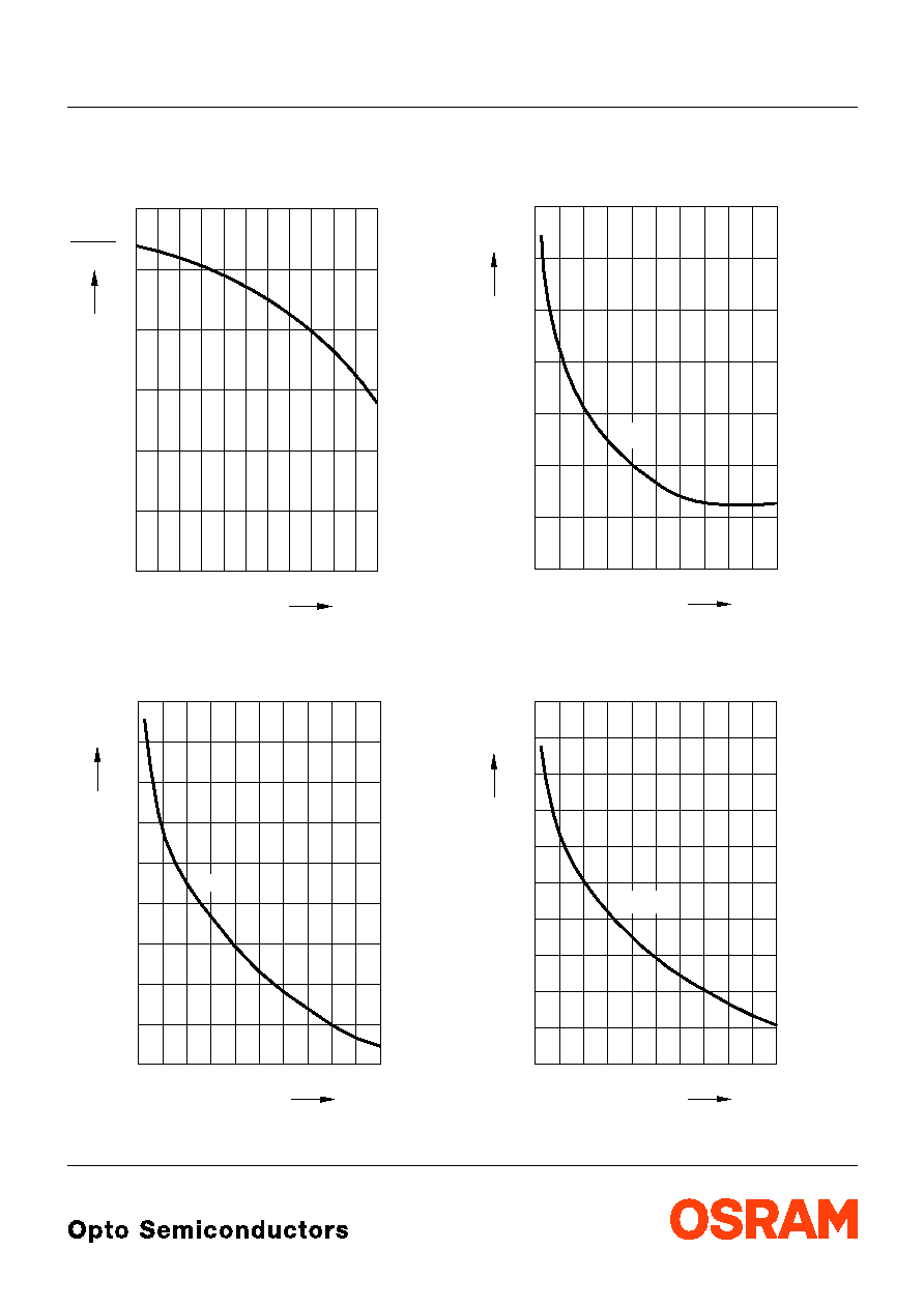
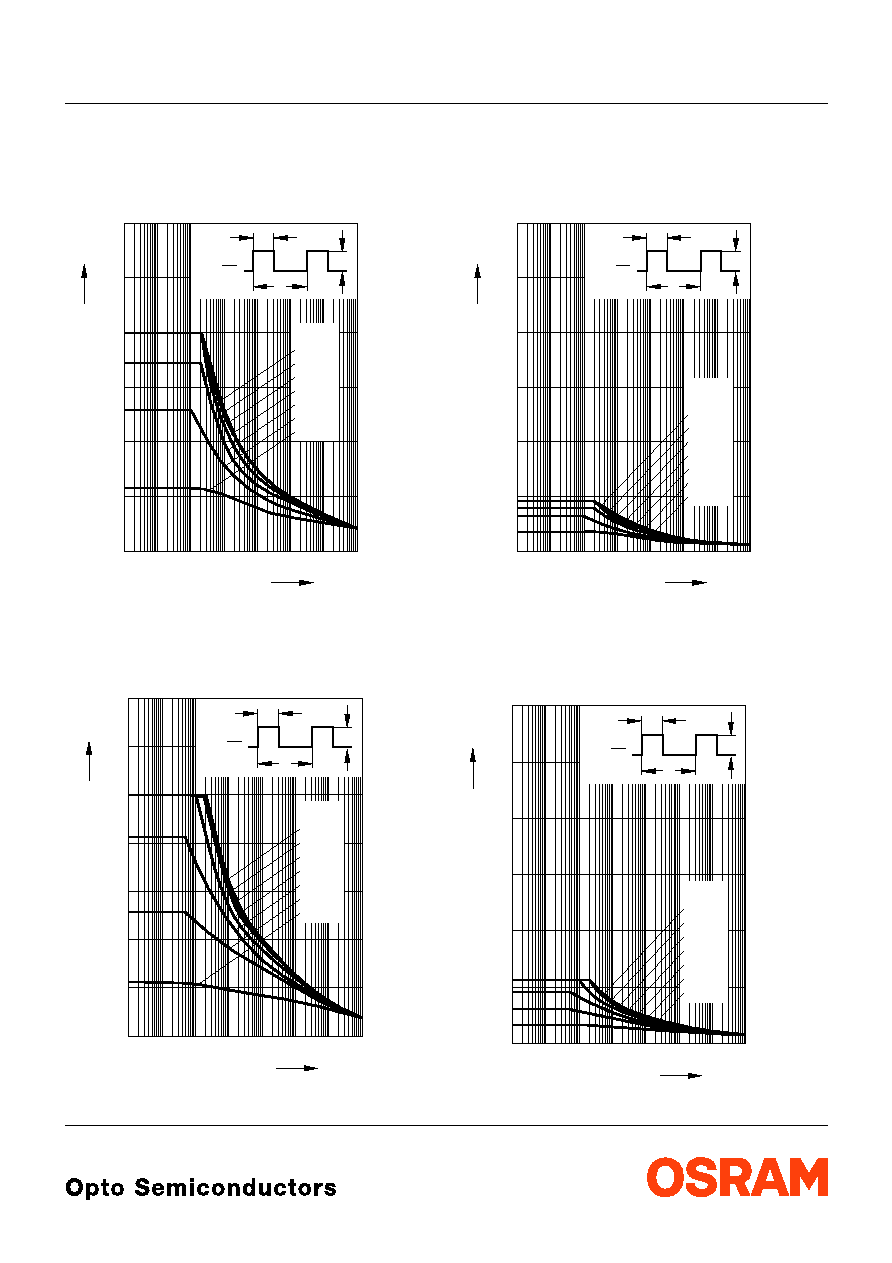
Zul‰ssige Impulsbelastbarkeit
I
F
=
f
(
t
p
)
Permissible Pulse Handling Capability
Duty cycle
D
= parameter,
T
A
= 25 ∞C
LB
Zul‰ssige Impulsbelastbarkeit
I
F
=
f
(
t
p
)
Permissible Pulse Handling Capability
Duty cycle
D
= parameter,
T
A
= 25 ∞C
LV, LT
Zul‰ssige Impulsbelastbarkeit
I
F
=
f
(
t
p
)
Permissible Pulse Handling Capability
Duty cycle
D
= parameter,
T
A
= 85 ∞C
LB
Zul‰ssige Impulsbelastbarkeit
I
F
=
f
(
t
p
)
Permissible Pulse Handling Capability
Duty cycle
D
= parameter,
T
A
= 85 ∞C
LV, LT
OHL01409
0
F
I
10
10
-5
-4
-3
10
10
-2
10
-1
10
0
s
10
1
10
2
p
t
0.05
0.10
0.15
0.20
0.25
0.30
0.05
0.5
0.2
0.1
D
0.02
0.01
0.005
=
A
D
T
t
=
P
t
T
P
I
F
OHL01411
0
F
I
10
10
-5
-4
-3
10
10
-2
10
-1
10
0
s
10
1
10
2
p
t
0.05
0.5
0.2
0.1
D
0.02
0.01
0.005
=
0.05
0.15
0.10
0.25
0.20
A
0.35
0.30
D
T
t
=
P
t
T
P
I
F
OHL01410
0
F
I
10
10
-5
-4
-3
10
10
-2
10
-1
10
0
s
10
1
10
2
p
t
0.05
0.10
0.15
0.20
0.25
0.30
0.05
0.5
0.2
0.1
D
0.02
0.01
0.005
=
A
D
T
t
=
P
t
T
P
I
F
OHL01412
0
F
I
10
10
-5
-4
-3
10
10
-2
10
-1
10
0
s
10
1
10
2
p
t
0.05
0.10
0.15
0.20
0.25
0.30
0.05
0.5
0.2
0.1
D
0.02
0.01
0.005
=
A
D
T
t
=
P
t
T
P
I
F
2001-03-01
10
LB 5413, LV 5413, LT 5413
Maþzeichnung
Package Outlines
Maþe werden wie folgt angegeben: mm (inch) / Dimensions are specified as follows: mm (inch).
Kathodenkennung:
k¸rzerer Lˆtspieþ
Cathode mark:
short solder lead
Gewicht / Approx. weight: 0.35 g
0.4 (0.016)
0.6 (0.024)
5.5 (0.217)
5.9 (0.232)
Area not flat
8.2 (0.323)
9.0 (0.354)
¯
4.8 (0.189)
¯
5.1 (0.201)
7.8 (0.307)
7.5 (0.295)
27.0 (1.063)
29.0 (1.142)
spacing
2.54 (0.100)
0.8 (0.031)
0.4 (0.016)
0.4 (0.016)
0.6 (0.024)
1.2 (0.047)
1.8 (0.071)
Cathode
GEXY6713
LB 5413, LV 5413, LT 5413
2001-03-01
11
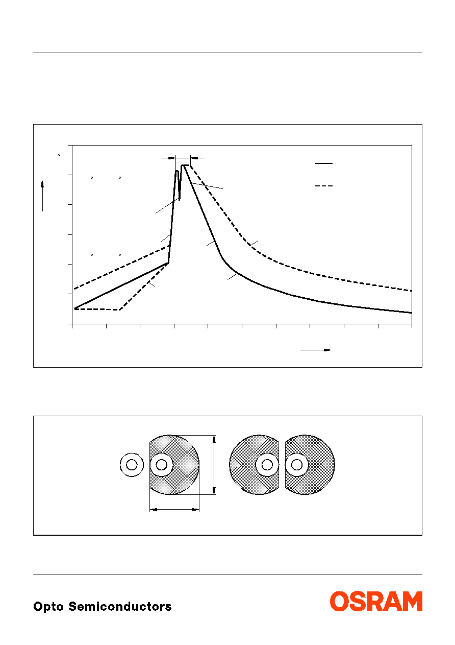
Lˆtbedingungen
Soldering Conditions
Wellenlˆten (TTW)(nach CECC 00802)
TTW Soldering(acc. to CECC 00802)
Empfohlenes Lˆtpaddesign
Wellenlˆten (TTW)
Recommended Solder Pad
TTW Soldering
Maþe werden wie folgt angegeben: mm (inch) / Dimensions are specified as follows: mm (inch).
OHLY0598
0
0
50
100
150
200
250
50
100
150
200
250
300
T
t
C
s
235 C
10 s
C
... 260
1. Welle
1. wave
2. Welle
2. wave
5 K/s
2 K/s
ca 200 K/s
C
C
... 130
100
2 K/s
Zwangsk¸hlung
forced cooling
Normalkurve
standard curve
Grenzkurven
limit curves
4 (0.157)
OHLPY985
4.8 (1.890)
2001-03-01
12
LB 5413, LV 5413, LT 5413
Published by OSRAM Opto Semiconductors GmbH & Co. OHG
Wernerwerkstrasse 2, D-93049 Regensburg
© All Rights Reserved.
Attention please!
The information describes the type of component and shall not be considered as assured characteristics.
Terms of delivery and rights to change design reserved. Due to technical requirements components may contain
dangerous substances. For information on the types in question please contact our Sales Organization.
If printed or downloaded, please find the latest version in the Internet.
Packing
Please use the recycling operators known to you. We can also help you ≠ get in touch with your nearest sales office.
By agreement we will take packing material back, if it is sorted. You must bear the costs of transport. For packing
material that is returned to us unsorted or which we are not obliged to accept, we shall have to invoice you for any costs
incurred.
Components used in life-support devices or systems must be expressly authorized for such purpose! Critical
components
1
may only be used in life-support devices or systems
2
with the express written approval of OSRAM OS.
1
A critical component is a component used in a life-support device or system whose failure can reasonably be expected
to cause the failure of that life-support device or system, or to affect its safety or the effectiveness of that device or
system.
2
Life support devices or systems are intended (a) to be implanted in the human body, or (b) to support and/or maintain
and sustain human life. If they fail, it is reasonable to assume that the health of the user may be endangered.
Revision History: 2001-03-01
Previous Version:
2001-03-01
Page
Subjects (major changes since last revision)