
Data Sheet
1
2001-04-09
2-Phase Stepper-Motor Driver
Bipolar-IC
TLE 4729 G
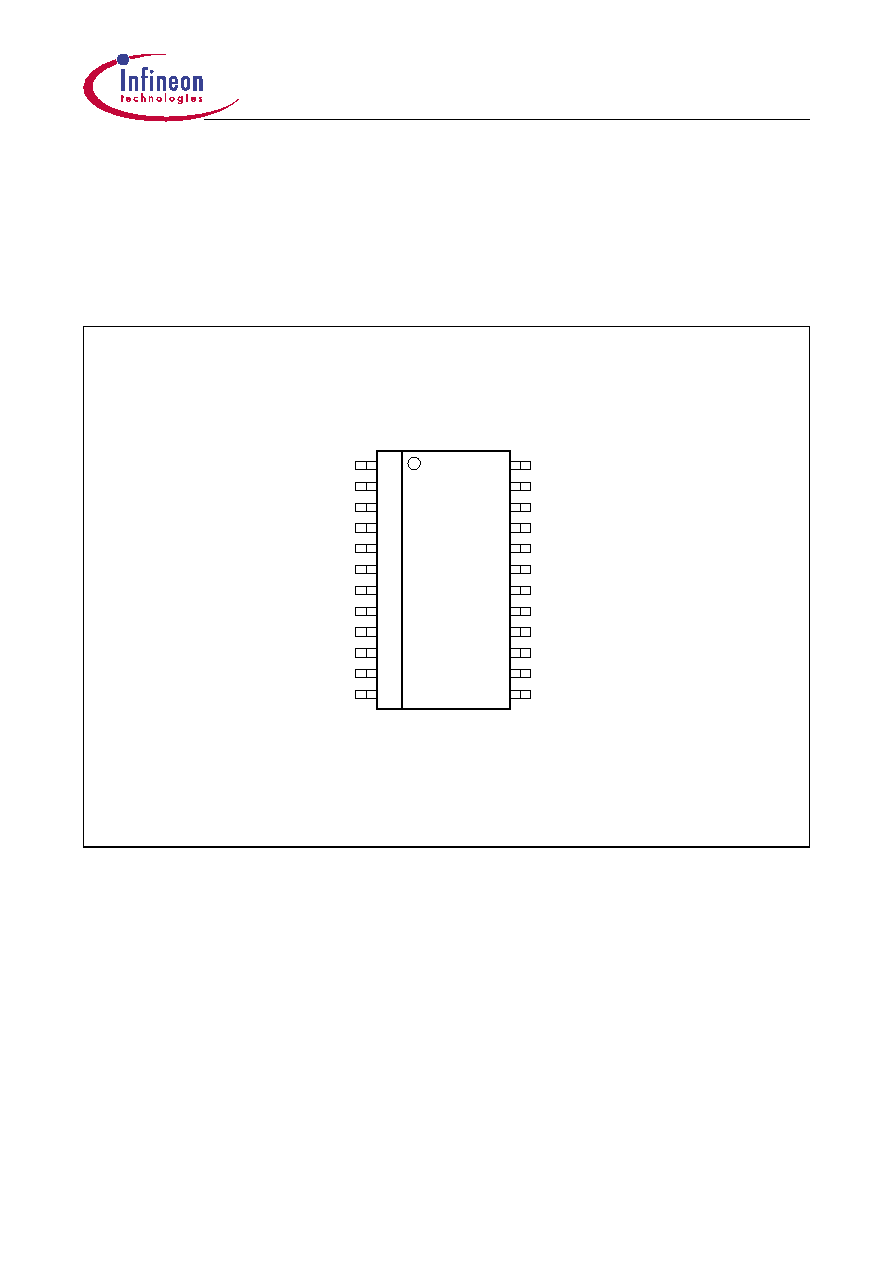
P-DSO-24-1, -3
Features
∑ 2
◊
0.7 amp. full bridge outputs
∑ Integrated driver, control logic and current control
(chopper)
∑ Very low current consumption in inhibit mode
∑ Fast free-wheeling diodes
∑ Max. supply voltage 45 V
∑ Output stages are free of crossover current
∑ Offset-phase turn-ON of output stages
∑ All outputs short-circuit proof
∑ Error-flag for overload, open load, over-temperature
∑ SMD package P-DSO-24-3
Functional Description
TLE 4729 G is a bipolar, monolithic IC for driving bipolar stepper motors, DC motors and
other inductive loads that operate by constant current. It is fully pin and function
compatible except the current programming is inverse to the TLE 4729 G with an
additional inhibit feature. The control logic and power output stages for two bipolar
windings are integrated on a single chip which permits switched current control of motors
with 0.7 A per phase at operating voltages up to 16 V.
The direction and value of current are programmable for each phase via separate control
inputs. In the case of low at all four current program inputs the device is switched to
inhibit mode automatically. A common oscillator generates the timing for the current
control and turn-on with phase offset of the two output stages. The two output stages in
full-bridge configuration include fast integrated freewheeling diodes and are free of
crossover current. The device can be driven directly by a microprocessor in several
modes by programming phase direction and current control of each bridge
independently.
Type
Ordering Code
Package
TLE 4729 G
Q67006-A9225
P-DSO-24-3 (SMD)
TLE 4729 G
Data Sheet
2
2001-04-09
With the two error outputs the TLE 4729 G signals malfunction of the device. Setting the
control inputs high resets the error flag and by reactivating the bridges one by one the
location of the error can be found.
Pin Configuration
(top view)
Figure 1
10
12
11
8
9
7
6
3
5
4
2
1
24
23
22
21
20
19
18
17
16
15
14
13
GND
OSC
GND
GND
GND
Q11
AEP02195
10
11
Phase 1
Q12
1
R
V
S
+
21
20
Phase 2
2
R
Error 1
GND
GND
GND
GND
Q21
Error 2
Q22
TLE 4729 G

TLE 4729 G
Data Sheet
3
2001-04-09
Pin Definitions and Functions
Pin
Function
1, 2, 23, 24
Digital control inputs
I
X0,
I
X1 for the magnitude of the current of the
particular phase.
1)
"No current" in both bridges inhibits the circuit and current consumption will sink below
50
µ
A (inhibit-mode)
3
Input phase 1; controls the current through phase winding 1.
On H-potential the phase current flows from Q11 to Q12, on L-potential
in the reverse direction.
5 ... 8,
17 ... 20
Ground; all pins are connected at leadframe internally.
4
Oscillator; works at approx. 25 kHz if this pin is wired to ground across
2.2 nF.
10
Resistor
R
1
for sensing the current in phase 1.
9, 12
Push-pull outputs Q11, Q12 for phase 1 with integrated free-wheeling
diodes.
11
Supply voltage; block to ground, as close as possible to the IC, with a
stable electrolytic capacitor of at least 47
µ
F in parallel with a ceramic
capacitor of 100 nF.
14
Error 2 output; signals with "low" the errors: short circuit to ground of
one or more outputs or over-temperature.
13, 16
Push-pull outputs Q22, Q21 for phase 2 with integrated free-wheeling
diodes.
15
Resistor
R
2
for sensing the current in phase 2.
21
Error 1 output; signals with "low" the errors: open load or short circuit to
+
V
S
of one or more outputs or short circuit of the load or over-
temperature.
22
Input phase 2; controls the current flow through phase winding 2. On
H-potential the phase current flows from Q21 to Q22, on L-potential in
the reverse direction.
I
set
= 450 mA with
R
sense
= 1
I
X1
I
X0
Phase Current
Example of Motor Status
L L
0
No current
1)
L H
0.155
◊
I
set
Hold
H L
I
set
Normal mode
H H
1.55
◊
I
set
Accelerate

TLE 4729 G
Data Sheet
4
2001-04-09
Block Diagram
Figure 2
D11
D12
D14
D13
T11
T13
T12
T14
Function
Logic
Phase 1
Oscillator
Phase 2
Function
Inhibit
Logic
T21
T23
D23
D21
T22
T24
D24
D22
Error-Flag
Generation
TLE 4729 G
Phase 1
Error 1
Phase 2
Error 2
V
S
+
Q21
Q22
21
20
OSC
C
OSC
V
+
S
R
1
R
2
Q11
Q12
R
sense
sense
R
GND
AEB02196
10
11
TLE 4729 G
Data Sheet
5
2001-04-09
Absolute Maximum Ratings
T
j
= ≠ 40 to 150
∞
C
Parameter
Symbol
Limit Values
Unit Remarks
min.
max.
Supply voltage
V
S
≠ 0.3
45
V
≠
Error outputs
V
Err
I
Err
≠ 0.3
≠
45
3
V
mA
≠
≠
Output current
I
Q
≠ 1
1
A
≠
Ground current
I
GND
≠ 2
≠
A
≠
Logic inputs
V
I
XX
≠ 15
15
V
I
XX; Phase 1, 2
Oscillator voltage
V
OSC
≠ 0.3
6
V
≠
R
1
, R
2
input voltage
V
RX
≠ 0.3
5
V
≠
Junction temperature
T
j
≠ 40
150
∞
C
Storage temperature
T
stg
≠ 50
150
∞
C
≠
Thermal resistances
Junction-ambient
Junction-ambient
(soldered on a 35
µ
m thick
20 cm
2
PC board copper
area)
Junction-case
R
th ja
R
th ja
R
th jc
≠
≠
≠
75
50
15
K/W
K/W
K/W
≠
≠
Measured on pin 5
Operating Range
Supply voltage
V
S
5
16
V
≠
Case temperature
T
C
≠ 40
110
∞
C
Measured on pin 5
P
diss
= 2 W
Output current
I
Q
≠ 800
800
mA
≠
Logic inputs
V
I
XX
≠ 5
+ 6
V
I
XX; Phase 1, 2
Error outputs
V
Err
I
Err
≠
0
25
1
V
mA
≠
≠

TLE 4729 G
Data Sheet
6
2001-04-09
Characteristics
V
S
= 6 to 16 V;
T
j
= ≠ 40 to 130
∞
C
Parameter
Symbol
Limit Values
Unit Test Condition
min.
typ.
max.
Current Consumption
From +
V
S
From +
V
S
I
S
I
S
≠
20
≠
30
50
50
µ
A
mA
I
XX = L;
V
S
= 12 V;
T
j
85
∞
C
I
Q1, 2
= 0 A
Oscillator
Output charging current
Charging threshold
Discharging threshold
Frequency
I
OSC
V
OSCL
V
OSCH
f
OSC
90
0.8
1.7
18
120
1.3
2.3
24
150
1.9
2.9
30
µ
A
V
V
kHz
≠
≠
≠
C
OSC
= 2.2 nF
Phase Current (
V
S
= 9 ... 16 V)
Mode "no current"
Voltage threshold of
current Comparator at
R
sense
in mode:
Hold
Setpoint
Accelerate
I
Q
V
ch
V
cs
V
ca
≠
40
410
630
0
70
450
700
≠
100
510
800
mA
mV
mV
mV
I
X0 = L;
I
X1 = L
I
X0 = H;
I
X1 = L
I
X0 = L;
I
X1 = H
I
X0 = H;
I
X1 = H
Logic Inputs (Phase X)
Threshold
Hysteresis
L-input current
L-input current
H-input current
V
I
V
IHy
I
IL
I
IL
I
IH
1.2
≠
≠ 10
≠ 100
≠ 1
1.7
200
≠ 1
≠ 20
0
2.2
≠
1
≠ 5
10
V
mV
µ
A
µ
A
µ
A
≠
≠
V
I
= 1.2 V
V
I
= 0 V
V
I
= 5 V
Logic Inputs (
I
X1;
I
X0)
Threshold
Hysteresis
L-input current
H-input current
V
I
V
IHy
I
IL
I
IH
0.8
≠
≠ 100
5
1.7
200
≠
20
2.2
≠
+ 5
50
V
mV
µ
A
µ
A
≠
≠
V
I
= 0 V
V
I
= 5 V

TLE 4729 G
Data Sheet
7
2001-04-09
Error Outputs
Saturation voltage
Leakage current
V
ErrSat
I
ErrL
50
≠
200
≠
500
10
mV
µ
A
I
Err
= 1 mA
V
Err
= 25 V
Thermal Protection
Shutdown
Prealarm
Delta
Hysteresis shutdown
Hysteresis prealarm
T
jsd
T
jpa
T
j
T
jsdhy
T
jpahy
140
120
10
≠
≠
150
130
20
20
20
160
140
30
≠
≠
∞
C
∞
C
K
K
K
I
Q1, 2
= 0 A
V
Err
= L
T
j
=
T
jsd
≠
T
jpa
≠
≠
Power Outputs
Diode Transistor Sink Pair
(D13, T13; D14, T14; D23, T23; D24, T24)
Saturation voltage
Saturation voltage
Reverse current
Forward voltage
Forward voltage
V
satI
V
satI
I
RI
V
FI
V
FI
0.1
0.2
500
0.6
0.7
0.3
0.5
1000
0.9
1.0
0.5
0.8
1500
1.2
1.3
V
V
µ
A
V
V
I
Q
= ≠ 0.45 A
I
Q
= ≠ 0.7 A
V
S
=
V
Q
= 40 V
I
Q
= 0.45 A
I
Q
= 0.7 A
Diode Transistor Source Pair
(T11, D11; T12, D12; T21, D21; T22, D22)
Saturation voltage
Saturation voltage
Saturation voltage
Saturation voltage
Reverse current
Forward voltage
Forward voltage
Diode leakage current
V
satuC
V
satuD
V
satuC
V
satuD
I
Ru
V
Fu
V
Fu
I
SL
0.6
0.1
0.7
0.2
400
0.7
0.8
0
1.0
0.3
1.2
0.5
800
1.0
1.1
3
1.2
0.6
1.5
0.8
1200
1.3
1.4
10
V
V
V
V
µ
A
V
V
mA
I
Q
= 0.45 A; charge
I
Q
= 0.45 A;
discharge
I
Q
= 0.7 A; charge
I
Q
= 0.7 A;
discharge
V
S
= 40 V,
V
Q
= 0 V
I
Q
= ≠ 0.45 A
I
Q
= ≠ 0.7 A
I
F
= ≠ 0.7 A
Characteristics (cont'd)
V
S
= 6 to 16 V;
T
j
= ≠ 40 to 130
∞
C
Parameter
Symbol
Limit Values
Unit Test Condition
min.
typ.
max.

TLE 4729 G
Data Sheet
8
2001-04-09
For details see next four pages.
These parameters are not 100% tested in production, but guaranteed by design.
Error Output Timing
Time Phase X to
I
XX
Time
I
XX to Phase X
Delay Phase X to Error 2
Delay Phase X to Error 1
Delay
I
XX to Error 2
Reset delay after Phase X
Reset delay after
I
XX
t
PI
t
IP
t
PEsc
t
PEol
t
IEsc
t
RP
t
RI
≠
≠
≠
≠
≠
≠
≠
5
12
45
15
30
3
1
20
100
100
50
80
10
5
µ
s
µ
s
µ
s
µ
s
µ
s
µ
s
µ
s
≠
Characteristics (cont'd)
V
S
= 6 to 16 V;
T
j
= ≠ 40 to 130
∞
C
Parameter
Symbol
Limit Values
Unit Test Condition
min.
typ.
max.

TLE 4729 G
Data Sheet
9
2001-04-09
Diagrams
Timing between
I
XX and Phase X to prevent setting the error flag
Operating conditions:
+
V
S
= 14 V,
T
j
= 25
∞
C,
I
err
= 1 mA, load = 3.3 mH, 1
If
t
PI
< typ. 5
µ
s, an error "open load" will be set.
If
t
IP
< typ. 12
µ
s, an error "open load" will be set.
t
PI
AET02197
Phase X
XX
a)
t
IP
Phase X
XX
AET02198
b)

TLE 4729 G
Data Sheet
10
2001-04-09
This time strongly depends on +
V
S
and inductivity of the load, see diagram below.
Time
t
IP
vs. Load Inductivity
Propagation Delay of the Error Flag
Operating conditions:
+
V
S
= 14 V,
T
j
= 25
∞
C,
I
err
= 1 mA, load = 3.3 mH, 1
20
10
0
0
20
5
10
15
40
30
60
mH
L
16 V
12 V
9 V
t
IP
s
µ
25
30
S
V = 6 V
AED02199
t
PEsc
Error 2
AED02200
Phase X
a)
I
XX = H, error condition: short circuit to GND.
typ.
t
PEsc
: 45
µ
s

TLE 4729 G
Data Sheet
11
2001-04-09
t
IEsc
is also measured under the condition: begin of short circuit to GND till error flag set.
t
PEol
Error 1
AET02201
Phase X
b)
I
XX = H, error condition: open load (equivalent: short circuit to +
V
S
).
typ.
t
PEol
: 15
µ
s
t
IEsc
Error 2
AET02202
XX
c) Phase X = H or L, const.; error condition: short circuit to GND.
typ.
t
IEsc
: 30
µ
s

TLE 4729 G
Data Sheet
12
2001-04-09
t
RP
AET02203
Error X
Phase x
d)
I
XX = H, reset of error flag when error condition is not true.
typ.
t
RP
: 3
µ
s
t
RI
AET02204
Error X
XX
typ.
t
RI
: 1
µ
s
e) Phase X = H or L, const.; reset of error flag when error condition is not true.
TLE 4729 G
Data Sheet
13
2001-04-09
Quiescent Current
I
S
vs. Supply Voltage
V
S
;
bridges not chopping;
T
j
= 25
∞
C
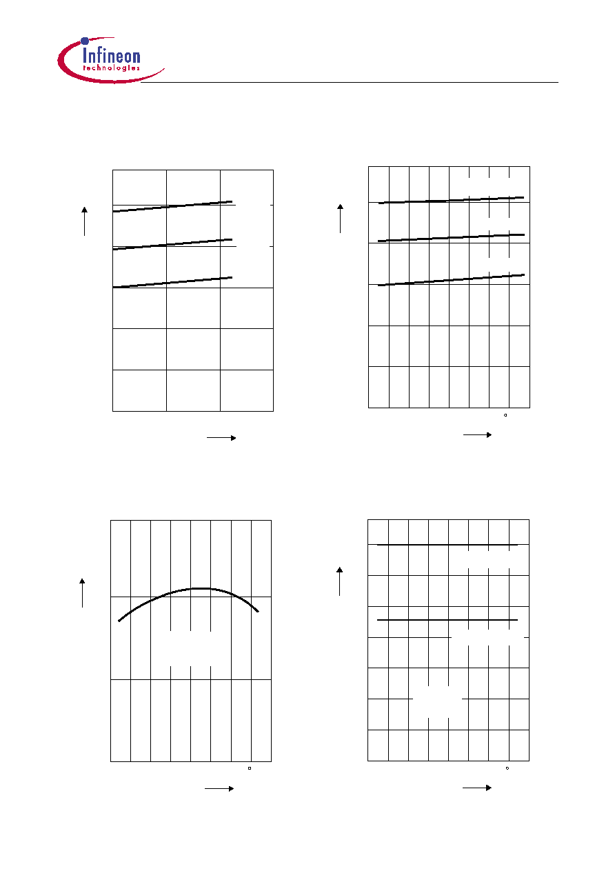
Oscillator Frequency
f
Osc
vs.
Junction Temperature
T
j
Quiesc. Current
I
S
vs. Junct. Temp.
T
j
;
bridges not chopping,
V
S
= 14 V
Output Current
I
QX
vs.
Junction Temperature
T
j
AED02205
5
0
V
mA
V
S
10
15
20
40
60
=
QX
0.70 A
20
10
30
50
S
0.45 A
0.07 A
-50
15
0
20
V
C
OSC
S
150
100
50
C
T
j
Osc
kHz
f
25
30
AED02207
= 14 V
= 2.2 nF
-50
0
0
10
20
30
150
100
50
C
T
j
0.07 A
S
mA
40
50
60
0.70 A
0.45 A
QX
=
AED02206
500
-50
0
0
300
100
400
200
R
X
V
S
= 14 V
150
100
50
C
T
j
700
800
600
QX
mA
X1 = H, X0 = H
AED02208
X1 = H, X0 = L
= 1

TLE 4729 G
Data Sheet
14
2001-04-09
Output Saturation Voltages
V
sat
vs. Output Current
I
Q
Typical Power Dissipation
P
tot
vs.
Output Current
I
Q
(non stepping)
Forward Current
I
F
of Free-Wheeling Diodes
vs. Forward Voltages
V
F
Permissible Power Dissipation
P
tot
vs.
Case Temp.
T
C
(measured at pin 5)
V
0
0
0.2
0.5
1.0
0.6
0.4
0.8
A
Q
satuD
V
V
satl
satuC
sat
V
= 14 V
V
1.5
V
T
j
S
= 25 C
2.0
AED02209
both phases active
0
0
0.2
1
2
0.6
0.4
0.8
A
Q
S
V = 14 V
tot
P
= 10 mH
L
OSC
phase x
phase x
C
3
T
C
W
R
= 25 C
= 2.2 nF
= 2
4
AED02211
AED02210
0
0
V
F
0.5
1.0
1.5
V
0.2
0.4
0.6
0.8
1.0
A
F
V
Fl
V
Fu
j
T = 25 ∞C
10
0
-25
0
25
6
2
4
8
125
75
C 175
T
C
120 C
jmax
T
150 C
=
tot
P
12
W
16
AED02212

TLE 4729 G
Data Sheet
15
2001-04-09
Input Characteristics of
I
XX
, Phase X
Quiescent Current
I
S
vs. Supply Voltage
V
S
;
inhibit mode;
T
j
= 25
∞
C
Output Leakage Current
-20
=
-120
-4
-6
-2
-60
-100
-40
-80
j
T
2
0
6
4 V
xx
V
40 C
25 C
150 C
xx
i
A
0
20
40
Phase X
xx
AED02213
µ
AED02215
5
0
100
50
0
10
15 V
S
250
200
150
S
20
µ
A
V
0
-0.8
-0.4
0
0.4
10
20
30 V
V
Q
40
S
V = 16 V
mA
0.8
R
1.2
S
V = 40 V
AED02214

TLE 4729 G
Data Sheet
16
2001-04-09
Figure 3
Application Circuit
Microcontroller
1
2
3
21
14
24
23
22
Phase 1
Error 1
Error 2
Phase 2
10
11
20
21
TLE 4729 G
M
Stepper
Motor
5,6,7,8,
17,18,19,20
10
15
4
R
2
1
1
1
R
22 nF
Q11
Q12
Q21
Q22
13
16
12
9
OSC
GND
S
V
100 nF
100
µ
F
11
+12V
AES02216

TLE 4729 G
Data Sheet
17
2001-04-09
Figure 4
Test Circuit
V
V
V
Err
2.2 nF
Osc
OSC
OSC
Error
Err
X
XX, Phase X
Rl
Fu
sense
V
C
SL
GND
GND
R
1
Rsense
V
Fl
Output
V
+
S
Q
satu
V
V
V
satl
AES02217
Ru
100 nF
100 F
S
V
S
µ
TLE 4729 G

TLE 4729 G
Data Sheet
18
2001-04-09
Figure 5
Full Step Operation
H
L
H
L
H
L
L
H
H
L
L
H
Phase 1
Q1
Q2
Phase 2
t
t
t
t
t
t
AED02218
t
t
accelerate mode
normal mode
acc
i
set
i
-
-
full step operation
21
20
11
10
acc
i
set
i
-
acc
i
-
set
i
i
set
acc
i

TLE 4729 G
Data Sheet
19
2001-04-09
Figure 6
Half Step Operation
AED02219
accelerate mode
normal mode
half step operation
21
20
Phase 2
L
L
H
H
H
L
Q2
-
-
-
i
set
acc
i
i
set
acc
i
acc
i
Q1
-
Phase 1
set
i
set
i
L
acc
i
H
10
11
H
H
L
L
t
t
t
t
t
t
t
t

TLE 4729 G
Data Sheet
20
2001-04-09
Figure 7
Current Control in Chop-Mode
V
Osc H
L
Osc
V
Osc
V
0
0
Rsense 1
Rsense
2
V
Q12
V
S
+
0
ca
V
S
+ V
Q11
V
V
+
S
V
Q22
+
V
Q21
V
S
Q1
i
acc
Q2
t
t
t
t
t
t
t
V
FU
satl
V
satu D
V
satu C
V
phase x
phase x
Operating conditions:
V
R
L
S
= 14 V
= 10 mH
= 4
= H
Phase x
AED02220
0
XX
= H
acc
i

TLE 4729 G
Data Sheet
21
2001-04-09
Figure 8
Phase Reversal and Inhibit
Osc
V
Rsense 1
S
+V
Q11
V
Phase 1
t
t
t
t
phase 1
phase 1
Operating conditions:
V
R
L
S
= L for t <
= 14 V
= 1 mH
= 4
= H for t >
AED02221
t
t
2.3 V
1.3 V
0 V
Oscillator
High Imped.
Phase change-over
H
L
Phase
0
High
Impedance
set
slow current decay
set
-
1
T
fast current
decay
=
2X
T
1
1
T
11
11
10
High
Impedance
+
V
Q12
V
S
slow current decay
= L

TLE 4729 G
Data Sheet
22
2001-04-09
Calculation of Power Dissipation
The total power dissipation
P
tot
is made up of
Saturation losses
P
sat
(transistor saturation voltage and diode forward voltages),
Quiescent losses
P
q
(quiescent current times supply voltage) and
Switching losses
P
s
(turn-ON / turn-OFF operations).
The following equations give the power dissipation for chopper operation without phase
reversal.
This is the worst case, because full current flows for the entire time and switching losses
occur in addition.
P
tot
= 2
◊
P
sat
+
P
q
+ 2
◊
P
s
where
P
sat
I
N
{
V
satI
◊
d
+
V
Fu
(1 ≠
d
) +
V
satuC
◊
d
+
V
satuD
(1 ≠
d
)}
P
q
=
I
q
◊
V
S
I
N
= Nominal current (mean value)
I
q
= Quiescent current
i
D
= Reverse current during turn-on delay
i
R
= Peak reverse current
t
p
= Conducting time of chopper transistor
t
ON
= Turn-ON time
t
OFF
= Turn-OFF time
t
DON
= Turn-ON delay
t
DOFF
= Turn-OFF delay
T
= Cycle duration
d
= Duty cycle
t
p
/
T
V
satl
= Saturation voltage of sink transistor (TX3, TX4)
V
satuC
= Saturation voltage of source transistor (TX1, TX2) during charge cycle
V
satuD
= Saturation voltage of source transistor (TX1, TX2) during discharge cycle
V
Fu
= Forward voltage of free-wheeling diode (DX1, DX2)
V
S
= Supply voltage
P
q
V
S
T
-------
i
D
t
DON
◊
2
-------------------------
i
D
i
R
+
(
)
t
ON
◊
4
--------------------------------------
I
N
2
-----
t
DOFF
t
OFF
+
(
)
+
+
Ó
˛
Ì
˝
Ï
¸

TLE 4729 G
Data Sheet
23
2001-04-09
Figure 9
Figure 10
Voltage and Current on Chopper Transistor
Dx3
Dx4
Dx1
Dx2
V
S
+
Tx3
Tx1
Tx4
Tx2
L
V
C
sense
R
AET02222
t
OFF
D OFF
t
P
t
ON
t
D ON
t
V
satl
N
Turn-OFF
Turn-ON
S
V
Fu
V
+
Fu
S
V + V
t
i
R
i
D
AET02223
Voltage and
Current on
Chopper
Transistor

TLE 4729 G
Data Sheet
24
2001-04-09
Application Hints
The TLE 4729 G is intended to drive both phases of a stepper motor. Special care has
been taken to provide high efficiency, robustness and to minimize external components.
Power Supply
The TLE 4729 G will work with supply voltages ranging from 5 V to 16 V at pin
V
S
.
Surges exceeding 16 V at
V
S
wont harm the circuit up to 45 V, but whole function is not
guaranteed. As soon as the voltage drops below approximately 16 V the TLE 4729 G
works promptly again.
As the circuit operates with chopper regulation of the current, interference generation
problems can arise in some applications. Therefore the power supply should be
decoupled by a 0.1
µ
F ceramic capacitor located near the package. Unstabilized
supplies may even afford higher capacities.
Inhibit Mode
In the case of low at all four current program inputs
I
XX the device will switch into inhibit
condition; the current consumption is reduced to very low values.
When starting operation again, i.e. putting at least one
I
XX to high potential, the Error 1
output signals an open load error if the corresponding phase input is high. The error is
reset by first recirculation in chop mode.
Current Sensing
The current in the windings of the stepper motor is sensed by the voltage drop across
R
sense
. Depending on the selected current internal comparators will turn off the sink
transistor as soon as the voltage drop reaches certain thresholds (typical 0 V, 0.07 V,
0.45 V and 0.7 V). These thresholds are not affected by variations of
V
S
. Consequently
instabilized supplies will not affect the performance of the regulation. For precise current
level it must be considered, that internal bounding wire (typ. 60 m
) is a part of
R
sense
.
Due to chopper control fast current rises (up to 10 A/
µ
s) will occur at the sensing
resistors. To prevent malfunction of the current sensing mechanism
R
sense
should be
pure ohmic. The resistors should be wired to GND as directly as possible. Capacitive
loads such as long cables (with high wire to wire capacity) to the motor should be
avoided for the same reason.
Synchronizing Several Choppers
In some applications synchrone chopping of several stepper motor drivers may be
desirable to reduce acoustic interference. This can be done by forcing the oscillator of
the TLE 4729 G by a pulse generator overdriving the oscillator loading currents
(approximately
±
120
µ
A). In these applications low level should be between 0 V and
0.8 V while high level should between 3 V and 5 V.

TLE 4729 G
Data Sheet
25
2001-04-09
Application Hints (cont'd)
Optimizing Noise Immunity
Unused inputs should always be wired to proper voltage levels in order to obtain highest
possible noise immunity.
To prevent crossconduction of the output stages the TLE 4729 G uses a special break
before make timing of the power transistors. This timing circuit can be triggered by short
glitches (some hundred nanoseconds) at the phase inputs causing the output stage to
become high resistive during some microseconds. This will lead to a fast current decay
during that time. To achieve maximum current accuracy such glitches at the phase
inputs should be avoided by proper control signals.
To lower EMI a ceramic capacitor of max. 3 nF is advisable from each output to GND.
Thermal Shut Down
To protect the circuit against thermal destruction, thermal shut down has been
implemented.
Error Monitoring
The error outputs signal corresponding to the logic table the errors described below.
Over-Temperature is implemented as pre-alarm; it appears approximately 20 K before
thermal shut down. To detect an open load, the recirculation of the inductive load is
watched. If there is no recirculation after a phase change-over, an internal error flipflop
is set. Because in most kinds of short circuits there won't flow any current through the
motor, there will be no recirculation after a phase change-over, and the error flipflop for
open load will be set, too. Additionally an open load error is signaled after a phase
change-over during hold mode.
Logic Table
Kind of Error
Error Output
Error 1
Error 2
a) No error
H
H
b) Short circuit to GND
H
L
c) Open load
1)
1)
Also possible: short circuit to +
V
S
or short circuit of the load.
L
H
d) b) and c) simultaneously
H
L
e) Temperature prealarm
L
L

TLE 4729 G
Data Sheet
26
2001-04-09
Only in the case of a short circuit to GND, the most probably kind of a short circuit in
automotive applications, the malfunction is signaled dominant (see d) in logic table) by
a separate error flag. Simultaneously the output current is disabled after 30
µ
s to prevent
disturbances.
A phase change-over or putting both current control inputs of the affected bridge on low
potential resets the error flipflop. Being a separate flipflop for every bridge, the error can
be located in easy way.

TLE 4729 G
Data Sheet
27
2001-04-09
Package Outlines
15.6
-0.4
24
13
1
12
Index Marking
1)
1.27
2)
0.35
+0.15
0.2 24x
-0.2
2.65 max
0.1
0.2
-0.1
2.45
1)
-0.2
7.6
0.35 x 45∞
8∞
max
0.23
+0.09
10.3
±0.3
0.4
+0.8
1) Does not include plastic or metal protrusions of 0.15 max rer side
2) Does not include dambar protrusion of 0.05 max per side
GPS05144
P-DSO-24-3
(Plastic Dual Small Outline Package)
SMD = Surface Mounted Device
Dimensions in mm
Sorts of Packing
Package outlines for tubes, trays etc. are contained in our
Data Book "Package Information".