
SCT 595
Low-Drop Voltage Regulator
Data Sheet
TLE 4295
Data Sheet Rev. 1.0
1
2002-02-13
Features
∑ Three versions: 3.0 V, 3.3 V, 5.0 V
∑ Output voltage tolerance
£ ± 4%
∑ Very low drop voltage
∑ Output current: 30 mA
∑ Power fail output
∑ Low quiescent current consumption
∑ Wide operation range: up to 45 V
∑ Wide temperature range: ≠ 40
∞C £
T
j
£ 150 ∞C
∑ Output protected against short circuit
∑ Overtemperature protection
∑ Reverse polarity proof
∑ Very small SMD-Package SCT-595
New type
Functional Description
The TLE 4295 G is a monolithic integrated low-drop voltage regulator in the very small
SMD package SCT-595. It is designed to supply e.g. microprocessor systems under the
severe conditions of automotive applications. Therefore the device is equipped with
additional protection functions against over load, short circuit and reverse polarity. At
overtemperature the regulator is automatically turned off by the integrated thermal
protection circuit.
Input voltages up to 40 V are regulated to
V
Q,nom
= 3.0 V (V30 version) 3.3 V (V33
version) or 5.0 V (V50 version). The output is able to drive a load of more than 30 mA
while it regulates the output voltage within a 4% accuracy.
The power fail output (open collector) is switched to low in case of undervoltage overload
or saturation of the output transistor.
Type
Ordering Code
Package
TLE 4295G V30
Q67006-A9410
SCT-595 (SMD)
TLE 4295G V33
Q67006-A9409
SCT-595 (SMD)
TLE 4295G V50
Q67006-A9395
SCT-595 (SMD)

TLE 4295
Data Sheet Rev. 1.0
2
2002-02-13
Figure 1
Pin Configuration (top view)
Pin Definitions and Functions
Pin No.
Symbol
Function
1
PF
Power Fail; L for under-voltage
2
GND
Ground; connected to pin 5
3
I
Input voltage
4
Q
Output voltage; must be blocked by a capacitor
C
Q
≥ 2.2 mF, ESR £ 5 W to GND
5
GND
Ground; connected to pin 2
AEP02661
5
4
1
2
3
GND
PF
Q
GND

TLE 4295
Data Sheet Rev. 1.0
3
2002-02-13
Figure 2
Block Diagram
Q
GND
PF
Temperature
Control
Band-Gap
Referenz
Control and
Protection
Saturation
Circuit
+
_
1
2, 5
4
3
AEB02662

TLE 4295
Data Sheet Rev. 1.0
4
2002-02-13
Note: Maximum ratings are absolute ratings; exceeding any one of these values may
cause irreversible damage to the integrated circuit.
Absolute Maximum Ratings
≠ 40
∞C <
T
j
< 150
∞C
Parameter
Symbol
Limit Values
Unit
Remarks
min.
max.
Input
Voltage
V
I
≠ 42
45
V
≠
Current
I
I
≠
≠
mA
internally limited
Output
Voltage
V
Q
≠ 6
30
V
≠
Current
I
Q
≠
≠
mA
internally limited
Power Fail
Voltage
V
PF
≠ 0.3
45
V
≠
Current
I
PF
≠ 500
*
mA
* internally limited
Temperatures
Junction temperature
T
j
≠ 40
150
∞C
≠
Storage temperature
T
stg
≠ 50
150
∞C
≠
Thermal Resistances
Junction pin
R
thj-pin
≠
30
K/W
measured to pin 5
Junction ambient
1)
R
thja
≠
179
K/W
zero airflow
zero heat sink area
1)
Worst case regarding peak temperature.

TLE 4295
Data Sheet Rev. 1.0
5
2002-02-13
Operating Range
Parameter
Symbol
Limit Values
Unit
Remarks
min.
max.
Input voltage
V
I
V
Q,nom
+ 0.5 V
45
V
≠
Output current
I
Q
≠
≠
mA
internally limited
Junction temperature
T
j
≠ 40
150
∞C
≠

TLE 4295
Data Sheet Rev. 1.0
6
2002-02-13
Electrical Characteristics
V
I
= 13.5 V; ≠ 40
∞C <
T
j
< 150
∞C; unless otherwise specified
Parameter
Symbol
Limit Values
Unit
Test Condition
min.
typ.
max.
Output
Output voltage
V30 version
V
Q
2.88
3.0
3.12
V
1 mA
<
I
Q
< 30 mA
V
I
= 13.5 V
Output voltage
V30 version
V
Q
2.88
3.0
3.12
V
I
Q
= 10 mA
4 V <
V
I
< 40 V
Output voltage
V33 version
V
Q
3.17
3.30
3.43
V
1 mA
<
I
Q
< 30 mA
V
I
= 13.5 V
Output voltage
V33 version
V
Q
3.17
3.30
3.43
V
I
Q
= 10 mA
4.3 V <
V
I
< 40 V
Output voltage
V50 version
V
Q
4.80
5.00
5.20
V
1 mA <
I
Q
< 30 mA
V
I
= 13.5 V
Output voltage
V50 version
V
Q
4.80
5.00
5.20
V
I
Q
= 10 mA
6 V <
V
I
< 40 V
Output current limitation
I
Q
30
≠
≠
mA
1)
Drop voltage
V
dr
≠
0.25
0.40
V
I
Q
= 20 mA
1)
Output capacitor
C
Q
2.2
≠
≠
mF
ESR
£ 5 W
at 10 kHz
Current Consumption
Current consumption
I
q
=
I
I
≠
I
Q
I
q
≠
2
4
mA
I
Q
< 30 mA
Current consumption
I
q
=
I
I
≠
I
Q
I
q
≠
120
200
mA
I
Q
< 1 mA

TLE 4295
Data Sheet Rev. 1.0
7
2002-02-13
Regulator Performance
Load regulation
|
,V
Q
|
≠
10
25
mV
1 mA
<
I
Q
<
25 mA;
T
j
= 25
∞C
Load regulation
|
,V
Q
|
≠
10
30
mV
1 mA
<
I
Q
<
25 mA
Line regulation
|
,V
Q
|
≠
5
25
mV
,V
I
=
V
Q,nom
+ 0.5 V
to 36 V;
I
Q
= 5 mA;
T
j
= 25
∞C
Line regulation
|
,V
Q
|
≠
10
30
mV
,V
I
=
V
Q,nom
+ 0.5 V
to 36 V;
I
Q
= 5 mA
Power-Supply-Ripple-
Rejection
PSRR
≠
60
≠
dB
f
r
= 100 Hz;
V
r
= 0.5
V
SS
Power Fail Output
Power fail threshold
V
QPF
≠
4.86
≠
V
TLE 4295GV50
≠
3.20
≠
V
TLE 4295GV33
≠
2.91
≠
V
TLE 4295GV30
Power Fail Headroom
V
Qnom
-
V
QPF
50
140
300
mV
TLE 4295GV50
33
100
200
mV
TLE 4295GV33
30
90
180
mV
TLE 4295GV30
Power fail low voltage
V
PFL
≠
150
300
mV
I
PF
= 0.1 mA
Pull up resistor
R
PF
70
100
130
k
W
internal connected to
V
Q
1)
Measured when the output voltage
V
Q
has dropped 100 mV from the nominal value.
Electrical Characteristics (cont'd)
V
I
= 13.5 V; ≠ 40
∞C <
T
j
< 150
∞C; unless otherwise specified
Parameter
Symbol
Limit Values
Unit
Test Condition
min.
typ.
max.

TLE 4295
Data Sheet Rev. 1.0
8
2002-02-13
Figure 3
Application Circuit
AES02663
TLE 4295G
4
3
1
2, 5
Q
PF
GND
Q
C
2.2
µ
F
C
100 nF
Power
Fail
3.0 V/3.3 V/5.0 V
V
Q, nom
+0.5 V to 45 V
TLE 4295
Data Sheet Rev. 1.0
9
2002-02-13
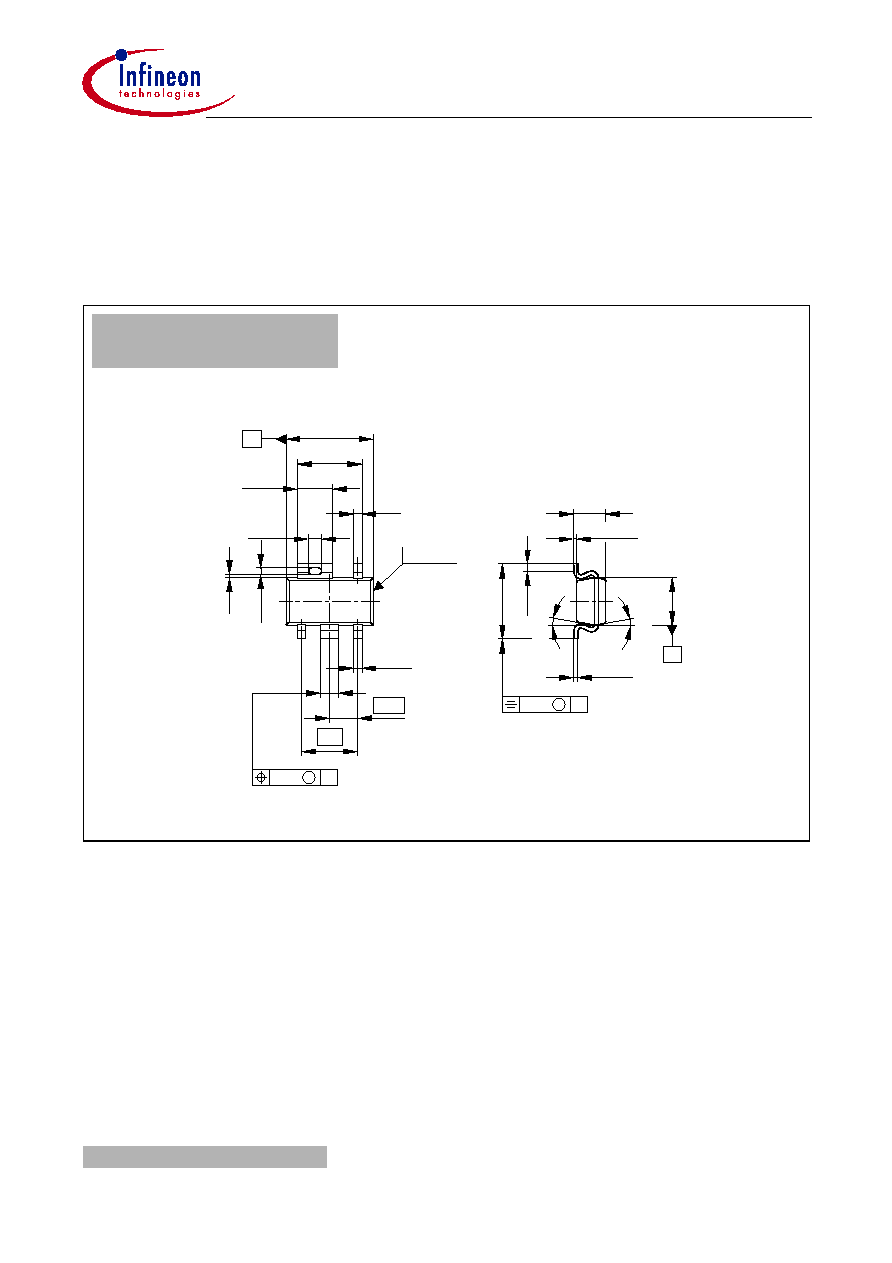
Package Outlines
acc. to
+0.2
1.9
0.6
-0.05
+0.1
+0.1
-0.05
0.3
B
A
0.25
M
B
1.1 max
2.6 max
10∞max
0.1 max
A
M
0.20
2.9
±0.2
1.6
±0.1
DIN 6784
(2.2)
(0.3)
1.2
-0.05
+0.1
0.95
-0.06
+0.1
0.15
10∞max
0.25 min
(0.4)
1)
(0.23)
1)
(0.13)
1)
Contour of slot depends on profile
of gull-wing lead form
3
4
5
2
1
SCT-595
(Plastic Dual Small Outline)
Sorts of Packing
Package outlines for tubes, trays etc. are contained in our
Data Book "Package Information".
Dimensions in mm
SMD = Surface Mounted Device

TLE 4295
Data Sheet Rev. 1.0
10
2002-02-13
Edition 2002-02-13
Published by Infineon Technologies AG,
St.-Martin-Strasse 53,
D-81541 M¸nchen, Germany
©
Infineon Technologies AG 2002.
All Rights Reserved.
Attention please!
The information herein is given to describe
certain components and shall not be consid-
ered as warranted characteristics.
Terms of delivery and rights to technical
change reserved.
We hereby disclaim any and all warranties,
including but not limited to warranties of non-
infringement, regarding circuits, descriptions
and charts stated herein.
Infineon Technologies is an approved CECC
manufacturer.
Information
For further information on technology, deliv-
ery terms and conditions and prices please
contact your nearest Infineon Technologies
Office in Germany or our Infineon Technolo-
gies Representatives worldwide (see ad-
dress list).
Warnings
Due to technical requirements components
may contain dangerous substances. For in-
formation on the types in question please
contact your nearest Infineon Technologies
Office.
Infineon Technologies Components may only
be used in life-support devices or systems
with the express written approval of Infineon
Technologies, if a failure of such components
can reasonably be expected to cause the fail-
ure of that life-support device or system, or to
affect the safety or effectiveness of that de-
vice or system. Life support devices or sys-
tems are intended to be implanted in the hu-
man body, or to support and/or maintain and
sustain and/or protect human life. If they fail, it
is reasonable to assume that the health of the
user or other persons may be endangered.