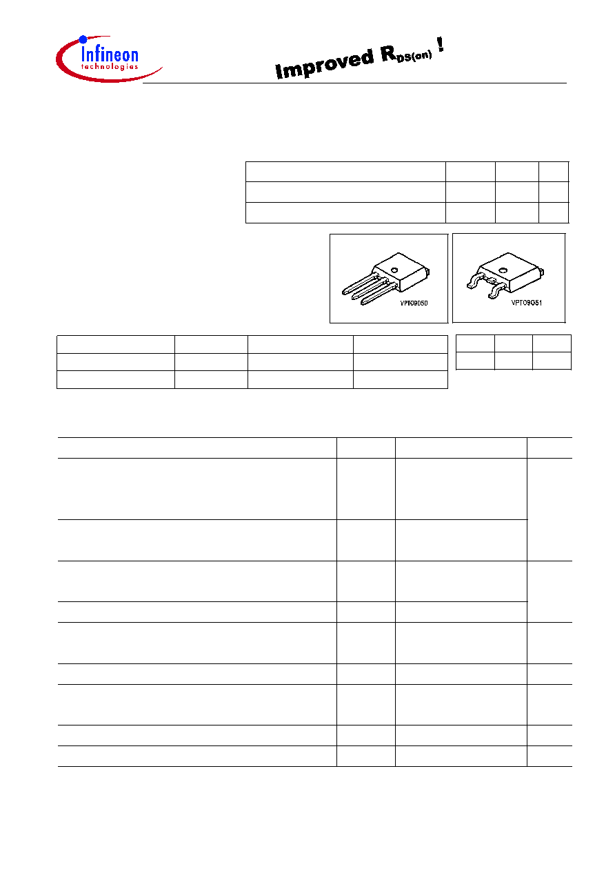
SPD 09N05
Data Sheet
1
06.99
SIPMOS
Æ
Power Transistor
Product Summary
Drain source voltage
55
V
DS
V
Drain-Source on-state resistance
0.1
R
DS(on)
I
D
Continuous drain current
9.2
A
Features
∑
N channel
∑
Enhancement mode
∑
Avalanche rated
∑
d
v/dt rated
∑
175∞C operating temperature
Pin 1
Pin 2
Pin 3
G
D
S
Packaging
Type
Package
Ordering Code
SPD09N05
Tape and Reel
P-TO252
Q67040-S4136
SPU09N05
Tube
Q67040-S4130-A2
P-TO251
MaximumRatings , at
Tj = 25 ∞C, unless otherwise specified
Parameter
Symbol
Unit
Value
Continuous drain current
T
C
= 25 ∞C
T
C
= 100 ∞C
9.2
6.5
I
D
A
Pulsed drain current
T
C
= 25 ∞C
I
Dpulse
37
Avalanche energy, single pulse
I
D
= 9.2 A,
V
DD
= 25 V,
R
GS
= 25
mJ
E
AS
35
Avalanche energy, periodic limited by
T
jmax
2.4
E
AR
Reverse diode d
v/dt
I
S
= 9.2 A,
V
DS
= 40 V, d
i/dt = 200 A/µs
d
v/dt
6
kV/µs
Gate source voltage
V
GS
±
20
V
Power dissipation
T
C
= 25 ∞C
P
tot
24
W
Operating and storage temperature
T
j ,
T
stg
∞C
-55... +175
55/175/56
IEC climatic category; DIN IEC 68-1

SPD 09N05
Data Sheet
2
06.99
Thermal Characteristics
Parameter
Values
Symbol
Unit
typ.
max.
min.
Characteristics
R
thJC
-
-
6.25
K/W
Thermal resistance, junction - case
-
Thermal resistance, junction - ambient, leded
R
thJA
-
100
-
-
-
-
75
50
SMD version, device on PCB:
@ min. footprint
@ 6 cm
2
cooling area
1)
R
thJA
Electrical Characteristics, at
Tj = 25 ∞C, unless otherwise specified
Parameter
Symbol
Unit
Values
min.
max.
typ.
Static Characteristics
Drain- source breakdown voltage
V
GS
= 0 V,
I
D
= 0.25 mA
-
V
(BR)DSS
55
-
V
Gate threshold voltage,
V
GS
=
V
DS
I
D
= 10 µA
V
GS(th)
4
3
2.1
Zero gate voltage drain current
V
DS
= 50 V,
V
GS
= 0 V,
T
j
= 25 ∞C
V
DS
= 50 V,
V
GS
= 0 V,
T
j
= 150 ∞C
-
-
I
DSS
µA
1
100
0.1
-
Gate-source leakage current
V
GS
= 20 V,
V
DS
= 0 V
I
GSS
-
10
nA
100
Drain-Source on-state resistance
V
GS
= 10 V,
I
D
= 6.5 A
R
DS(on)
-
0.093
0.1
1 Device on 40mm*40mm*1.5mm epoxy PCB FR4 with 6 cm2 (one layer, 70µm thick) copper area for drain
connection. PCB is vertical without blown air.

SPD 09N05
Data Sheet
3
06.99
Electrical Characteristics, at
Tj = 25 ∞C, unless otherwise specified
Parameter
Symbol
Values
Unit
min.
typ.
max.
Dynamic Characteristics
Transconductance
V
DS
2*
I
D
*
R
DS(on)max
,
I
D
= 6.5 A
g
fs
3
4.5
-
S
Input capacitance
V
GS
= 0 V,
V
DS
= 25 V,
f = 1 MHz
C
iss
-
215
270
pF
Output capacitance
V
GS
= 0 V,
V
DS
= 25 V,
f = 1 MHz
C
oss
-
75
95
Reverse transfer capacitance
V
GS
= 0 V,
V
DS
= 25 V,
f = 1 MHz
C
rss
-
45
60
Turn-on delay time
V
DD
= 30 V,
V
GS
= 10 V,
I
D
= 9.2 A,
R
G
= 50
t
d(on)
-
15
25
ns
Rise time
V
DD
= 30 V,
V
GS
= 10 V,
I
D
= 9.2 A,
R
G
= 50
t
r
-
20
30
Turn-off delay time
V
DD
= 30 V,
V
GS
= 10 V,
I
D
= 9.2 A,
R
G
= 50
t
d(off)
-
30
45
Fall time
V
DD
= 30 V,
V
GS
= 10 V,
I
D
= 9.2 A,
R
G
= 50
t
f
-
25
40

SPD 09N05
Data Sheet
4
06.99
Electrical Characteristics, at
Tj = 25 ∞C, unless otherwise specified
Parameter
Symbol
Values
Unit
min.
typ.
max.
Dynamic Characteristics
Gate to source charge
V
DD
= 40 V,
I
D
= 9.2 A
2
nC
1.3
Q
gs
-
-
3.5
Q
gd
Gate to drain charge
V
DD
= 40 V,
I
D
= 9.2 A
5.25
Gate charge total
V
DD
= 40 V,
I
D
= 9.2 A,
V
GS
= 0 to 10 V
-
7
11
Q
g
Gate plateau voltage
V
DD
= 40 V,
I
D
= 9.2 A
V
(plateau)
5.9
-
V
-
Reverse Diode
Inverse diode continuous forward current
T
C
= 25 ∞C
I
S
-
-
9.2
A
Inverse diode direct current,pulsed
T
C
= 25 ∞C
I
SM
-
-
37
Inverse diode forward voltage
V
GS
= 0 V,
I
F
= 18.5 A
V
SD
-
1.05
V
1.8
Reverse recovery time
V
R
= 30 V,
I
F
=
I
S
, d
i
F
/d
t = 100 A/µs
t
rr
-
50
ns
75
Reverse recovery charge
V
R
= 30 V,
I
F=
l
S
, d
i
F
/d
t = 100 A/µs
Q
rr
-
µC
0.085
0.13
SPD 09N05
Data Sheet
5
06.99
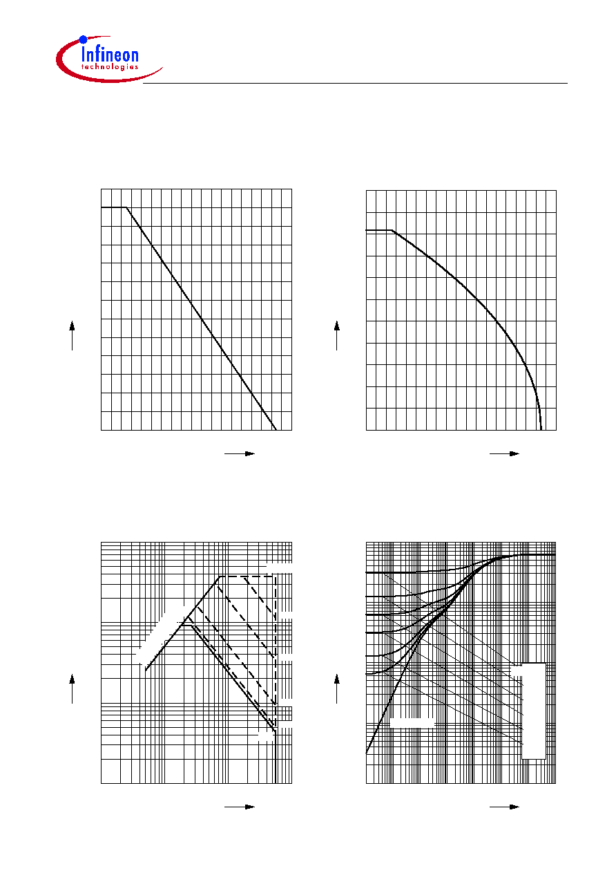
Power Dissipation
P
tot
=
f (T
C
)
0
20
40
60
80
100 120 140 160 ∞C 190
T
C
0
2
4
6
8
10
12
14
16
18
20
22
W
26
SPD09N05
P
tot
Drain current
I
D
=
f (T
C
)
parameter:
V
GS
10 V
0
20
40
60
80
100 120 140 160 ∞C 190
T
C
0
1
2
3
4
5
6
7
8
9
A
11
SPD09N05
I
D
Transient thermal impedance
Z
thJC
=
f (t
p
)
parameter :
D = t
p
/
T
10
-7
10
-6
10
-5
10
-4
10
-3
10
-2
10
0
s
t
p
-3
10
-2
10
-1
10
0
10
1
10
K/W
SPD09N05
Z
thJC
single pulse
0.01
0.02
0.05
0.10
0.20
D = 0.50
Safe operating area
I
D
=
f (V
DS
)
parameter :
D = 0 , T
C
= 25 ∞C
10
-1
10
0
10
1
10
2
V
V
DS
-1
10
0
10
1
10
2
10
A
SPD09N05
I
D
R
DS(on)
=
V
DS
/
I
D
DC
10 ms
1 ms
100 µs
10 µs
t
p
= 2.5µs
SPD 09N05
Data Sheet
6
06.99
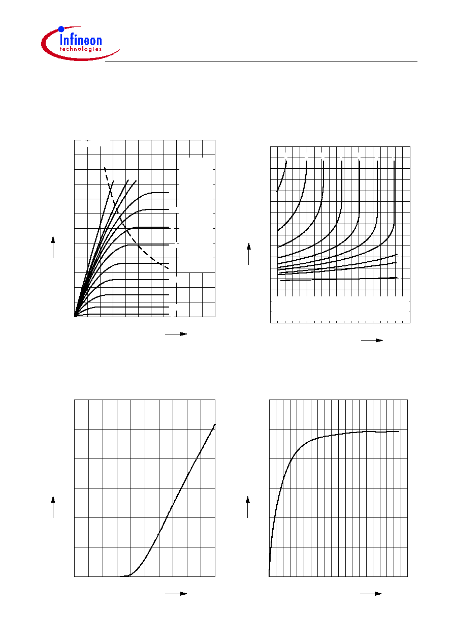
Typ. output characteristics
I
D
=
f (V
DS
)
parameter:
t
p
= 80 µs
0.0
1.0
2.0
3.0
4.0
V
5.5
V
DS
0
2
4
6
8
10
12
14
16
18
20
A
24
SPD09N05
I
D
V
GS
[V]
a
a
4.0
b
b
4.5
c
c
5.0
d
d
5.5
e
e
6.0
f
f
6.5
g
g
7.0
h
h
7.5
i
i
8.0
j
j
9.0
k
k
10.0
l
P
tot
= 24W
l
20.0
Typ. drain-source-on-resistance
R
DS(on)
=
f (I
D
)
parameter:
V
GS
0
2
4
6
8
10
12
14
16 A
19
I
D
0.00
0.04
0.08
0.12
0.16
0.20
0.24
0.32
SPD09N05
R
DS(on)
V
GS
[V] =
c
c
5.0
d
d
5.5
e
e
6.0
f
f
6.5
g
g
7.0
h
h
7.5
i
i
8.0
j
j
9.0
k
k
10.0
l
l
20.0
Typ. transfer characteristics
I
D
=
f (V
GS
)
parameter:
t
p
= 80 µs
V
DS
2 x
I
D
x
R
DS(on) max
0
1
2
3
4
5
6
7
8
V
10
V
GS
0
5
10
15
20
A
30
I
D
Typ. forward transconductance
g
fs
= f(I
D
)
; T
j
= 25∞C
parameter:
g
fs
0
2
4
6
8
10
12
14
16
A
20
I
D
0
1
2
3
4
S
6
g
fs
SPD 09N05
Data Sheet
7
06.99
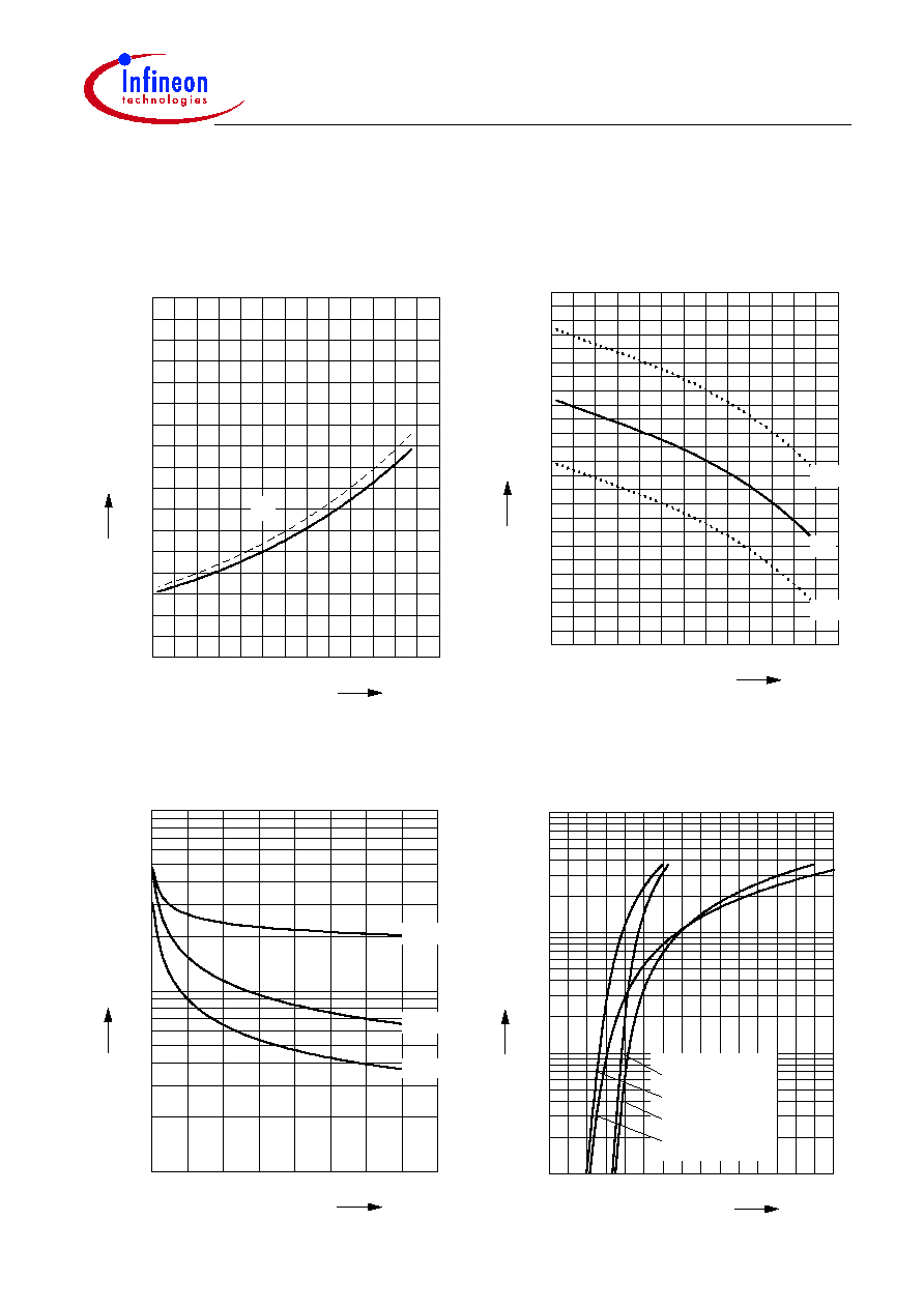
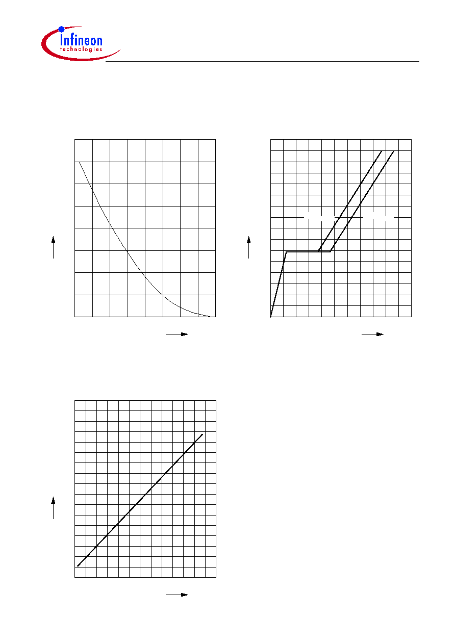
Drain-source on-resistance
R
DS(on)
=
f (T
j
)
parameter :
I
D
= 6.5 A,
V
GS
= 10 V
-60
-20
20
60
100
140
∞C
200
T
j
0.00
0.04
0.08
0.12
0.16
0.20
0.24
0.28
0.34
SPD09N05
R
DS(on)
typ
98%
Gate threshold voltage
V
GS(th)
=
f (T
j
)
parameter :
V
GS
=
V
DS
,
I
D
= 10 µA
-60
-20
20
60
100
140
V
200
T
j
0.0
0.4
0.8
1.2
1.6
2.0
2.4
2.8
3.2
3.6
4.0
4.4
V
5.0
V
GS(th)
min
typ
max
Typ. capacitances
C =
f (V
DS
)
parameter:
V
GS
= 0 V,
f = 1 MHz
0
5
10
15
20
25
30
V
40
VDS
1
10
2
10
3
10
pF
C
Ciss
Coss
Crss
Forward characteristics of reverse diode
I
F
=
f (V
SD
)
parameter:
T
j
,
t
p
= 80 µs
0.0
0.4
0.8
1.2
1.6
2.0
2.4
V
3.0
V
SD
-1
10
0
10
1
10
2
10
A
SPD09N05
I
F
T
j
= 25 ∞C typ
T
j
= 25 ∞C (98%)
T
j
= 175 ∞C typ
T
j
= 175 ∞C (98%)
SPD 09N05
Data Sheet
8
06.99
Typ. gate charge
V
GS
=
f (Q
Gate
)
parameter:
I
D puls
= 9.2 A
0
2
4
6
8
nC
11
Q
Gate
0
2
4
6
8
10
12
V
16
SPD09N05
V
GS
DS max
V
0,8
DS max
V
0,2
Avalanche Energy
E
AS
=
f (T
j
)
parameter:
I
D
= 9.2 A,
V
DD
= 25 V
R
GS
= 25
20
40
60
80
100
120
140
∞C
180
T
j
0
5
10
15
20
25
30
mJ
40
E
AS
Drain-source breakdown voltage
V
(BR)DSS
=
f (T
j
)
-60
-20
20
60
100
140
∞C
200
T
j
50
52
54
56
58
60
62
64
V
66
SPD09N05
V
(BR)DSS