2000-05-29
Page 1
SPP06N80C2
Preliminary data
Cool MOSTM
Power Transistor
C
Power Semiconductors
O
O L
MOS
Feature
∑
New revolutionary high voltage technology
∑
Ultra low gate charge
∑
Periodic avalanche rated
∑
Extreme d
v/dt rated
∑
Ultra low effective capacitances
∑
Improved noise immunity
Product Summary
V
DS
800
V
R
DS(on)
900
m
W
I
D
6
A
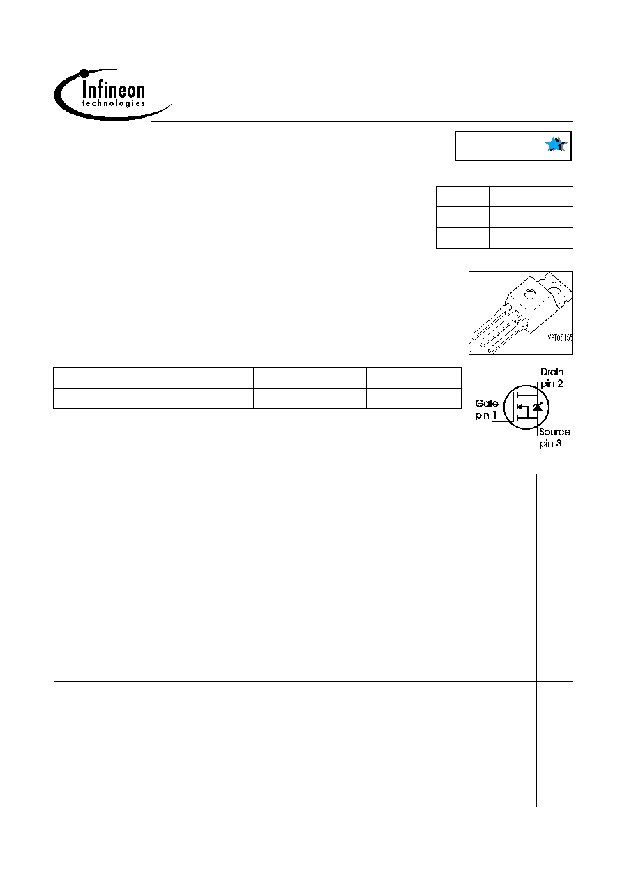
P-TO220-3-1
Type
Package
Ordering Code
SPP06N80C2
P-TO220-3-1
Q67040-S4351
Marking
SPP06N80C2
Maximum Ratings, at
T
j
= 25 ∞C, unless otherwise specified
Parameter
Symbol
Value
Unit
Continuous drain current
T
C
= 25 ∞C
T
C
= 100 ∞C
I
D
6
3.8
A
Pulsed drain current,
t
p
limited by
T
jmax
I
D puls
18
Avalanche energy, single pulse
I
D
=1.5A,
V
DD
=50V
E
AS
230
mJ
Avalanche energy, repetitive
t
AR
limited by
T
jmax
1)
I
D
=6A,
V
DD
=50V
E
AR
0.2
Avalanche current, repetitive
t
AR
limited by
T
jmax
I
AR
6
A
Reverse diode d
v/dt
I
S
=6A,
V
DS
<
V
DD
, d
i/dt=100A/µs, T
jmax
=150∞C
d
v/dt
6
V/ns
Gate source voltage
V
GS
±20
V
Power dissipation
T
C
= 25 ∞C
P
tot
83
W
Operating and storage temperature
T
j ,
T
stg
-55... +150
∞C

2000-05-29
Page 2
SPP06N80C2
Preliminary data
Thermal Characteristics
Parameter
Symbol
Values
Unit
min.
typ.
max.
Characteristics
Thermal resistance, junction - case
R
thJC
-
-
1.5
K/W
Thermal resistance, junction - ambient, leaded
R
thJA
-
-
62
Linear derating factor
-
-
0.67
W/K
Soldering temperature,
1.6 mm (0.063 in.) from case for 10s
T
sold
-
-
260
∞C
Electrical Characteristics, at
T
j
= 25 ∞C, unless otherwise specified
Static Characteristics
Drain-source breakdown voltage
V
GS
=0V,
I
D
=0.25mA
V
(BR)DSS
800
-
-
V
Drain-source avalanche breakdown voltage
V
GS
=0V,
I
D
=6A
V
(BR)DS
-
870
-
Gate threshold voltage,
V
GS
=
V
DS
I
D
=250µA
V
GS(th)
2
3
4
Zero gate voltage drain current
V
DS
= 800 V,
V
GS
= 0 V,
T
j
= 25 ∞C
V
DS
= 800 V,
V
GS
= 0 V,
T
j
= 150 ∞C
I
DSS
-
-
0.5
-
10
100
µA
Gate-source leakage current
V
GS
=20V,
V
DS
=0V
I
GSS
-
-
100
nA
Drain-source on-state resistance
V
GS
=10V,
I
D
=3.8A,
T
j
=25∞C
R
DS(on)
-
780
900
m
W
Gate input resistance
f = 1 MHz, open drain
R
G
-
0.7
-
W
1Repetitve avalanche causes additional power losses that can be calculated as P
AV
=
E
AR
*
f.

2000-05-29
Page 3
SPP06N80C2
Preliminary data
Electrical Characteristics , at
T
j
= 25 ∞C, unless otherwise specified
Parameter
Symbol
Conditions
Values
Unit
min.
typ.
max.
Characteristics
Transconductance
g
fs
V
DS
≥
2*
I
D
*
R
DS(on)max
,
I
D
=3.8A
-
4
-
S
Input capacitance
C
iss
V
GS
=0V,
V
DS
=25V,
f=1MHz
-
785
-
pF
Output capacitance
C
oss
-
390
-
Reverse transfer capacitance
C
rss
-
20
-
Effective output capacitance,
1)
energy related
C
o(er)
V
GS
=0V,
V
DS
=0V to 640 V
-
22
-
pF
Effective output capacitance,
2)
time related
C
o(tr)
-
42
-
Turn-on delay time
t
d(on)
V
DD
=400V,
V
GS
=0/10V,
I
D
=6A,
R
G
=12
W
,
T
j
=125∞C
-
25
-
ns
Rise time
t
r
-
15
-
Turn-off delay time
t
d(off)
-
48
60
Fall time
t
f
-
8
13
Gate Charge Characteristics
Gate to source charge
Q
gs
V
DD
=640V,
I
D
=6A
-
2.5
-
nC
Gate to drain charge
Q
gd
-
9.8
-
Gate charge total
Q
g
V
DD
=640V,
I
D
=6A,
V
GS
=0 to 10V
-
19.4
25
Gate plateau voltage
V
(plateau)
V
DD
=640V,
I
D
=6A
-
6
-
V
1C
o(er)
is a fixed capacitance that gives the same stored energy as
C
oss
while
V
DS
is rising from 0 to 80%
V
DSS
.
2C
o(tr)
is a fixed capacitance that gives the same charging time as
C
oss
while
V
DS
is rising from 0 to 80%
V
DSS
.
2000-05-29
Page 4
SPP06N80C2
Preliminary data
Electrical Characteristics, at
T
j
= 25 ∞C, unless otherwise specified
Parameter
Symbol
Conditions
Values
Unit
min.
typ.
max.
Reverse Diode
Inverse diode continuous
forward current
I
S
T
C
=25∞C
-
-
6
A
Inverse diode direct current,
pulsed
I
SM
-
-
18
Inverse diode forward voltage
V
SD
V
GS
=0V,
I
F
=
I
S
-
1
1.2
V
Reverse recovery time
t
rr
V
R
=400V,
I
F
=
I
S
,
d
i
F
/d
t=100A/µs
-
520
-
ns
Reverse recovery charge
Q
rr
-
5
-
µC
Peak reverse recovery current
I
rrm
-
17
-
A
Peak rate of fall of reverse
recovery current
di
rr
/
dt
-
400
-
A/µs
Transient Thermal Characteristics
Symbol
Value
Unit
Symbol
Value
Unit
typ.
typ.
Transient thermal impedance
Thermal resistance
R
th1
0.023
K/W
R
th2
0.033
R
th3
0.067
R
th4
0.189
R
th5
0.208
R
th6
0.076
Thermal capacitance
C
th1
0.000135
Ws/K
C
th2
0.000438
C
th3
0.000313
C
th4
0.00149
C
th5
0.00738
C
th6
0.068
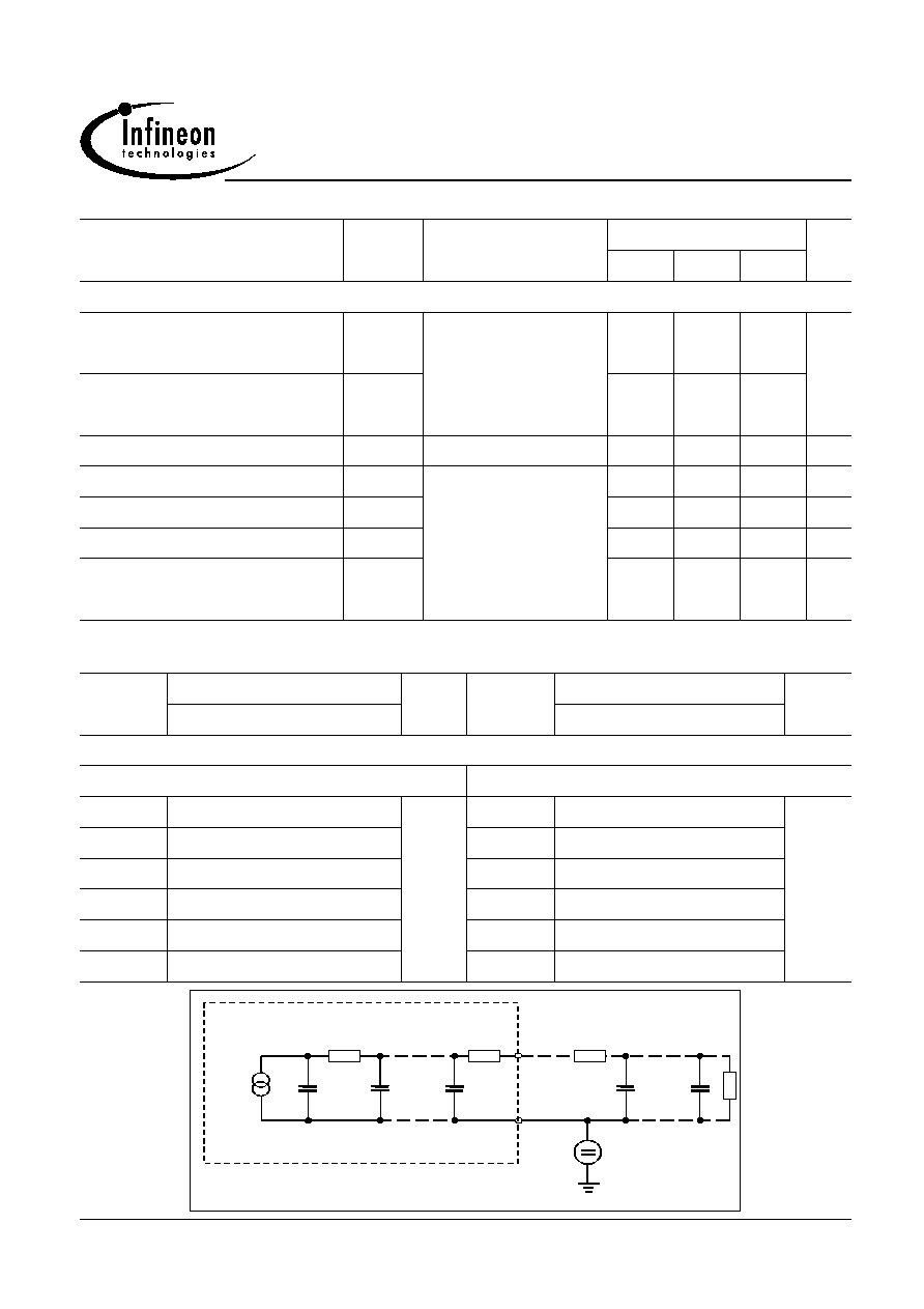
E xternal H eatsink
T
j
T
case
T
am b
C
th1
C
th2
R
th1
R
th,n
C
th,n
P
tot
(t)
2000-05-29
Page 5
SPP06N80C2
Preliminary data
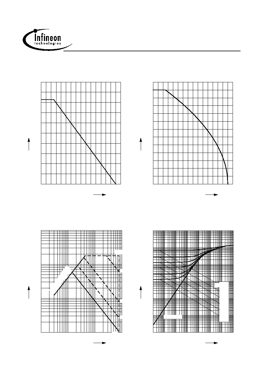
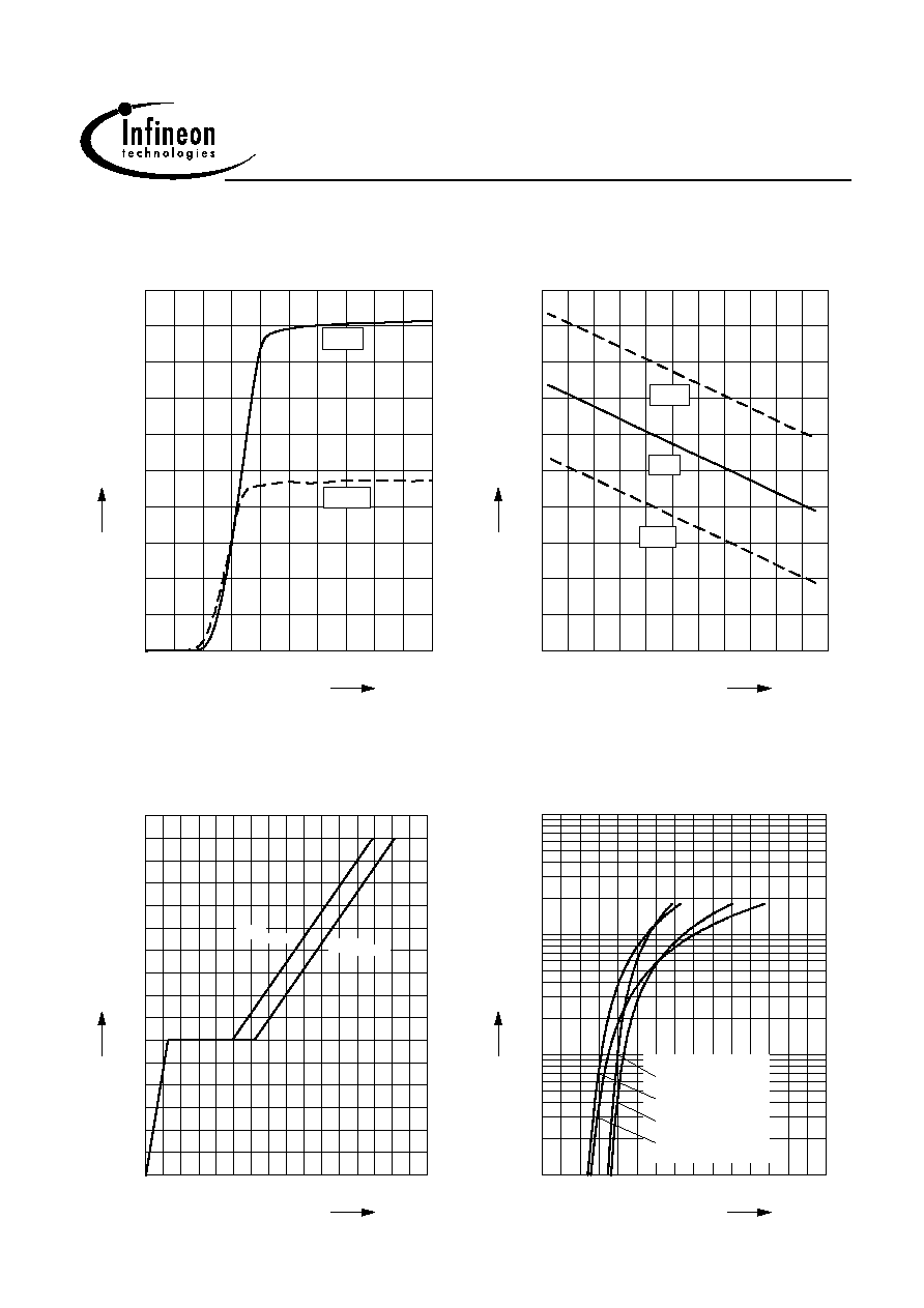
1 Power dissipation
P
tot
=
f (T
C
)
0
20
40
60
80
100
120
∞C
160
T
C
0
10
20
30
40
50
60
70
80
W
100
SPP06N80C2
P
tot
2 Drain current
I
D
=
f (T
C
)
parameter:
V
GS
≥
10 V
0
20
40
60
80
100
120
∞C
160
T
C
0.0
0.5
1.0
1.5
2.0
2.5
3.0
3.5
4.0
4.5
5.0
5.5
A
6.5
SPP06N80C2
I
D
4 Transient thermal impedance
Z
thJC
=
f (t
p
)
parameter :
D = t
p
/
T
10
-7
10
-6
10
-5
10
-4
10
-3
10
-2
10
0
s
t
p
-5
10
-4
10
-3
10
-2
10
-1
10
0
10
1
10
K/W
SPP06N80C2
Z
thJC
single pulse
0.01
0.02
0.05
0.10
0.20
D = 0.50
3 Safe operating area
I
D
=
f ( V
DS
)
parameter :
D = 0 , T
C
=25∞C
10
0
10
1
10
2
10
3
V
V
DS
-1
10
0
10
1
10
2
10
A
SPP06N80C2
I
D
R
D
S
(o
n)
=
V
D
S
/
I
D
DC
10 ms
1 ms
100 µs
t
p
= 32.0µs
2000-05-29
Page 6
SPP06N80C2
Preliminary data
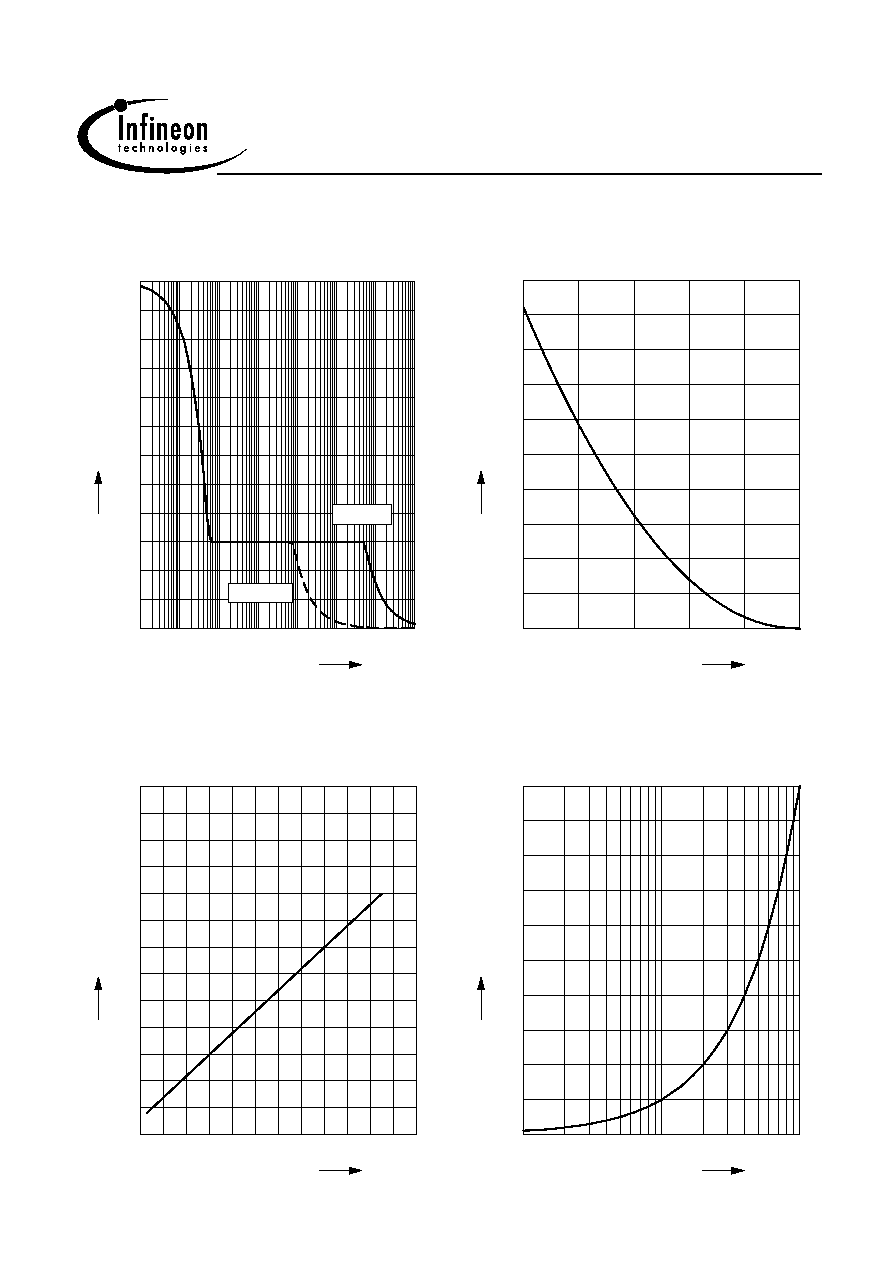
5 Typ. output characteristic
I
D
=
f (V
DS
);
T
j
=25∞C
parameter:
t
p
= 10 µs,
V
GS
0
5
10
15
20
V
30
V
DS
0
2
4
6
8
10
12
14
16
A
20
I
D
5V
6V
7V
8V
20V
10V
6 Typ. output characteristic
I
D
=
f (V
DS
);
T
j
=150∞C
parameter:
t
p
= 10 µs,
V
GS
0
5
10
15
20
V
30
V
DS
0
1
2
3
4
5
6
7
8
9
A
11
I
D
4V
4.5V
5V
5.5V
6V
7V
20V
10V
8V
7 Typ. drain-source on resistance
R
DS(on)
=
f(I
D
)
parameter:
T
j
=150∞C,
V
GS
0
2
4
6
8
A
11
I
D
1.0
1.5
2.0
2.5
3.0
3.5
4.0
W
5.0
R
DS
(
on)
4V
4.5V
5V
5.5V
6V
7V
8V
10V
20V
8 Drain-source on-state resistance
R
DS(on)
=
f (T
j
)
parameter :
I
D
= 3.8 A,
V
GS
= 10 V
-60
-20
20
60
100
∞C
180
T
j
0.0
0.5
1.0
1.5
2.0
2.5
3.0
3.5
4.0
4.5
W
5.5
SPP06N80C2
R
DS(on)
typ
98%
2000-05-29
Page 7
SPP06N80C2
Preliminary data
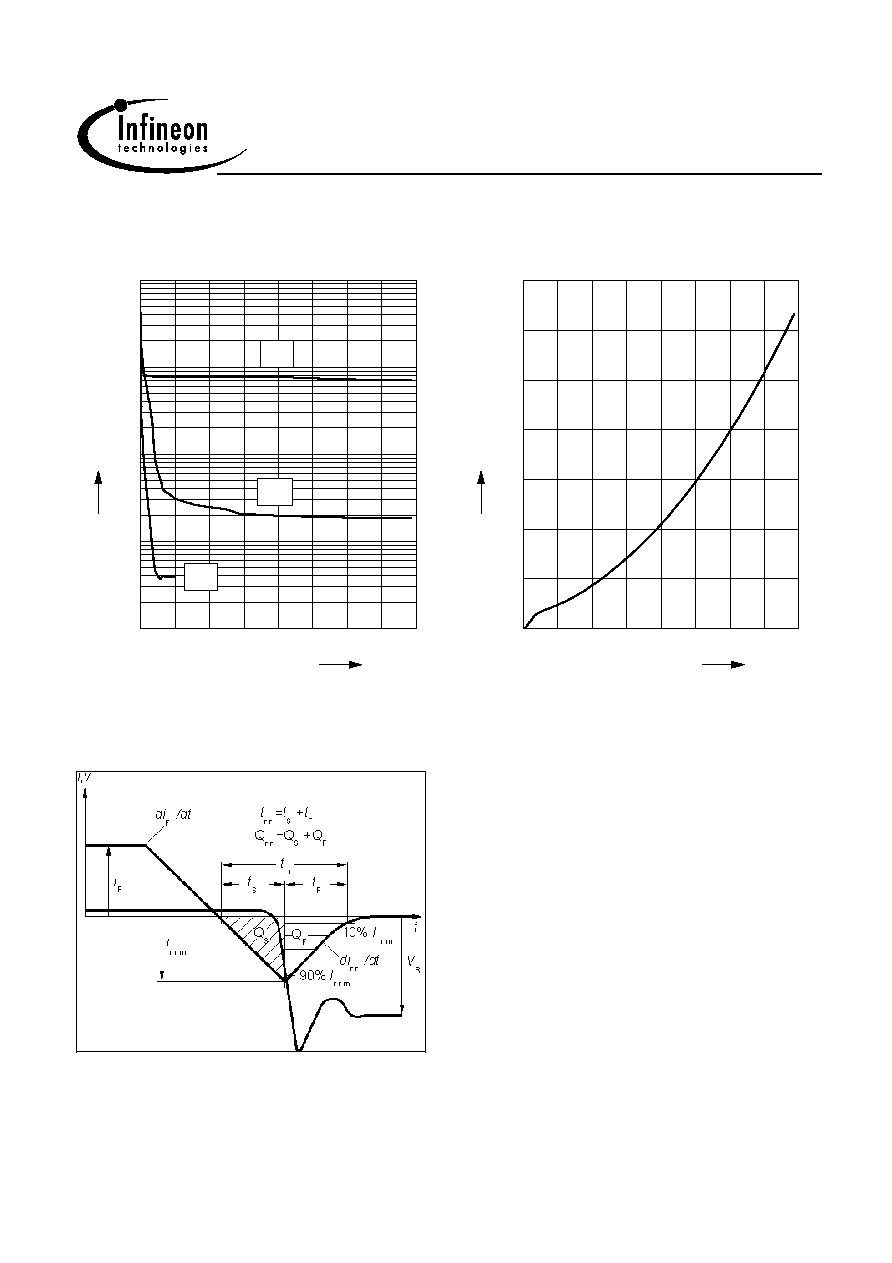
9 Typ. transfer characteristics
I
D
=
f ( V
GS
);
V
DS
≥
2 x
I
D
x
R
DS(on)max
parameter:
t
p
= 10 µs
0
2
4
6
8
10
12
14
16
V
20
V
GS
0
2
4
6
8
10
12
14
16
A
20
I
D
25∞C
150∞C
10 Gate threshold voltage
V
GS(th)
=
f (T
j
)
parameter:
V
GS
=
V
DS
,
I
D
= 250 µA
-60
-20
20
60
100
∞C
160
T
j
0.0
0.5
1.0
1.5
2.0
2.5
3.0
3.5
4.0
V
5.0
V
GS(th)
min.
typ.
max.
11 Typ. gate charge
V
GS
= f (Q
Gate
)
parameter:
I
D
= 6 A pulsed
0
4
8
12
16
20
24
nC
32
Q
Gate
0
2
4
6
8
10
12
V
16
SPP06N80C2
V
GS
0,8
V
DS max
DS max
V
0,2
12 Forward characteristics of body diode
I
F
=
f (V
SD
)
parameter:
Tj , t
p
= 10 µs
0.0
0.4
0.8
1.2
1.6
2.0
2.4
V
3.0
V
SD
-1
10
0
10
1
10
2
10
A
SPP06N80C2
I
F
T
j
= 25 ∞C typ
T
j
= 25 ∞C (98%)
T
j
= 150 ∞C typ
T
j
= 150 ∞C (98%)
2000-05-29
Page 8
SPP06N80C2
Preliminary data
14 Avalanche energy
E
AS
=
f (T
j
)
par.:
I
D
= 1.5 A,
V
DD
= 50 V
25
50
75
100
∞C
150
T
j
0
25
50
75
100
125
150
175
200
mJ
250
E
AS
13 Avalanche SOA
I
AR
=
f (t
AR
)
par.:
T
j
£
150 ∞C
10
-3
10
-2
10
-1
10
0
10
1
10
2
10
4
µs
t
AR
0.0
0.5
1.0
1.5
2.0
2.5
3.0
3.5
4.0
4.5
5.0
A
6.0
I
AR
T
j(START)
=125∞C
T
j(START)
=25∞C
15 Drain-source breakdown voltage
V
(BR)DSS
=
f (T
j
)
-60
-20
20
60
100
∞C
180
T
j
720
740
760
780
800
820
840
860
880
900
920
940
V
980
SPP06N80C2
V
(BR)DSS
16 Avalanche power losses
P
AR
=
f (f )
parameter:
E
AR
=0.2mJ
10
4
10
5
10
6
MHz
f
0
20
40
60
80
100
120
140
160
W
200
P
AR
2000-05-29
Page 9
SPP06N80C2
Preliminary data
17 Typ. capacitances
C = f (V
DS
)
parameter:
V
GS
=0V,
f=1 MHz
0
100
200
300
400
500
600
V
800
V
DS
0
10
1
10
2
10
3
10
4
10
pF
C
C
iss
C
oss
C
rss
18 Typ.
C
oss
stored energy
E
oss
=
f(V
DS
)
0
100
200
300
400
500
600
V
800
V
DS
0
1
2
3
4
5
µJ
7
E
oss
Definition of diodes switching characteristics
2000-05-29
Page 10
SPP06N80C2
Preliminary data
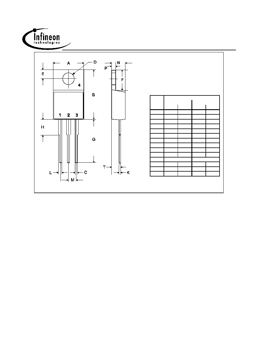
P-TO220-3-1
symbol
[mm]
[inch]
min
max
min
max
A
9.70
10.30
0.3819
0.4055
B
14.88
15.95
0.5858
0.6280
C
0.65
0.86
0.0256
0.0339
D
3.55
3.89
0.1398
0.1531
E
2.60
3.00
0.1024
0.1181
F
6.00
6.80
0.2362
0.2677
G
13.00
14.00
0.5118
0.5512
H
4.35
4.75
0.1713
0.1870
K
0.38
0.65
0.0150
0.0256
L
0.95
1.32
0.0374
0.0520
M
N
4.30
4.50
0.1693
0.1772
P
1.17
1.40
0.0461
0.0551
T
2.30
2.72
0.0906
0.1071
2.54 typ.
0.1 typ.
dimensions
P-TO220-3-1

2000-05-29
Page 11
SPP06N80C2
Preliminary data
Published by
Infineon Technologies AG,
Bereichs Kommunikation
St.-Martin-Strasse 53,
D-81541 M¸nchen
© Infineon Technologies AG 1999
All Rights Reserved.
Attention please!
The information herein is given to describe certain components and shall not be considered as warranted
characteristics.
Terms of delivery and rights to technical change reserved.
We hereby disclaim any and all warranties, including but not limited to warranties of non-infringement,
regarding circuits, descriptions and charts stated herein.
Infineon Technologies is an approved CECC manufacturer.
Information
For further information on technology, delivery terms and conditions and prices please contact your nearest
Infineon Technologies Office in Germany or our Infineon Technologies Reprensatives worldwide (see address list).
Warnings
Due to technical requirements components may contain dangerous substances.
For information on the types in question please contact your nearest Infineon Technologies Office.
Infineon Technologies Components may only be used in life-support devices or systems with the express
written approval of Infineon Technologies, if a failure of such components can reasonably be expected to
cause the failure of that life-support device or system, or to affect the safety or effectiveness of that device
or system Life support devices or systems are intended to be implanted in the human body, or to support
and/or maintain and sustain and/or protect human life. If they fail, it is reasonable to assume that the health
of the user or other persons may be endangered.