2001-09-07
Page 1
SDP20S30
SDB20S30
Preliminary data
Silicon Carbide Schottky Diode
Revolutionary semiconductor
material - Silicon Carbide
Switching behavior benchmark
No reverse recovery
No temperature influence on
the switching behavior
No forward recovery
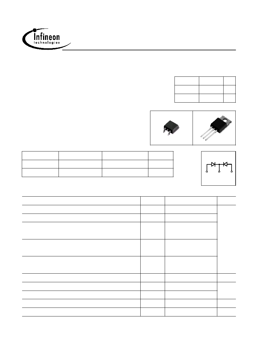
Product Summary
V
RRM
300
V
Q
c
23
nC
I
F
2x10
A
P-TO220-3-1.
P-TO220-3.SMD
Marking
D20S30
S20S30
Type
Package
Ordering Code
SDP20S30
P-TO220-3-1.
Q67040-S4419
SDB20S30
P-TO220-3.SMD Q67040-S4374
1
2 3
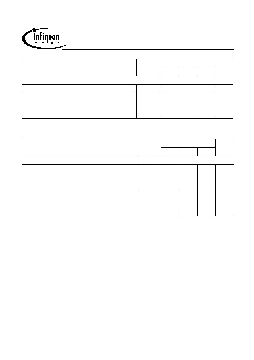
Maximum Ratings,at T
j
= 25 ∞C, unless otherwise specified (per leg)
Parameter
Symbol
Value
Unit
Continuous forward current,
T
C
=100∞C
I
F
10
A
RMS forward current
,
f
=50Hz
I
FRMS
14
Surge non repetitive forward current, sine halfwave
T
C
=25∞C, t
p
=10ms
I
FSM
36
Repetitive peak forward current
T
j
=150∞C, T
C
=100∞C, D=0.1
I
FRM
45
Non repetitive peak forward current
t
p
=10µs, T
C
=25∞C
I
FMAX
100
i
2
t value
,
T
C
=25∞C, t
p
=10ms
i
2
dt
6.5
A≤s
Repetitive peak reverse voltage
V
RRM
300
V
Surge peak reverse voltage
V
RSM
300
Power dissipation, single diode mode
,
T
C
=25∞C
P
tot
65
W
Operating and storage temperature
T
j ,
T
stg
-55... +175
∞C
2001-09-07
Page 2
SDP20S30
SDB20S30
Preliminary data
Thermal Characteristics
Parameter
Symbol
Values
Unit
min.
typ.
max.
Characteristics
Thermal resistance, junction - case (per leg)
R
thJC
-
-
2.3
K/W
SMD version, device on PCB:
P-TO263-3-2: @ min. footprint
P-TO263-3-2: @ 6 cm
2
cooling area
1)
R
thJA
-
-
-
35
62
-
Electrical Characteristics, at T
j
= 25 ∞C, unless otherwise specified (per leg)
Parameter
Symbol
Values
Unit
min.
typ.
max.
Static Characteristics
Diode forward voltage
I
F
=10A, T
j
=25∞C
I
F
=10A, T
j
=150∞C
V
F
-
-
1.5
1.5
1.7
1.9
V
Reverse current
V
R
=300V, T
j
=25∞C
V
R
=300V, T
j
=150∞C
I
R
-
-
15
20
200
1000
µA
1Device on 40mm*40mm*1.5mm epoxy PCB FR4 with 6cm≤ (one layer, 70 µm thick) copper area for drain
connection. PCB is vertical without blown air.
2001-09-07
Page 3
SDP20S30
SDB20S30
Preliminary data
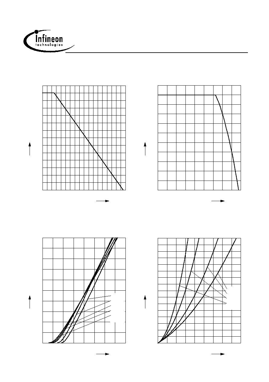
Electrical Characteristics,at T
j
= 25 ∞C, unless otherwise specified (per leg)
Parameter
Symbol
Values
Unit
min.
typ.
max.
AC Characteristics
Total capacitive charge
1)
V
R
=200V, I
F
=10A, di
F
/dt
=-200A/µs, T
j
=150∞C
Q
c
-
23
-
nC
Switching time
2)
V
R
=200V, I
F
=10A, di
F
/dt
=-200A/µs, T
j
=150∞C
t
rr
-
n.a.
-
ns
Total capacitance
V
R
=0V, T
C
=25∞C, f=1MHz
V
R
=150V, T
C
=25∞C, f=1MHz
V
R
=300V, T
C
=25∞C, f=1MHz
C
-
-
-
600
55
40
-
-
-
pF
2001-09-07
Page 4
SDP20S30
SDB20S30
Preliminary data
1 Power dissipation (per leg)
P
tot
= f (T
C
)
0
20
40
60
80
100 120 140
∞C
180
T
C
0
5
10
15
20
25
30
35
40
45
50
55
60
W
70
P
tot
2 Diode forward current (per leg)
I
F
= f (T
C
)
parameter: T
j
175 ∞C
0
20
40
60
80
100 120 140
∞C
180
T
C
0
1
2
3
4
5
6
7
8
9
A
11
I
F
4 Typ. forward power dissipation vs.
average forward current (per leg)
P
F(AV)=f(I
F
)
T
C
=100∞C, d = t
p
/T
0
2
4
6
8
10
12
14
A
18
I
F(AV)
0
4
8
12
16
20
24
W
32
P
F(AV)
d=1
d=0.5
d=0.2
d=0.1
3 Typ. forward characteristic (per leg)
I
F
= f (V
F
)
parameter: Tj , t
p
= 350 µs
0.6
0.8
1
1.2
1.4
1.6
1.8
V
2.2
V
F
0
2
4
6
8
10
12
14
16
A
20
I
F
-40∞C
25∞C
100∞C
125∞C
150∞C
2001-09-07
Page 5
SDP20S30
SDB20S30
Preliminary data
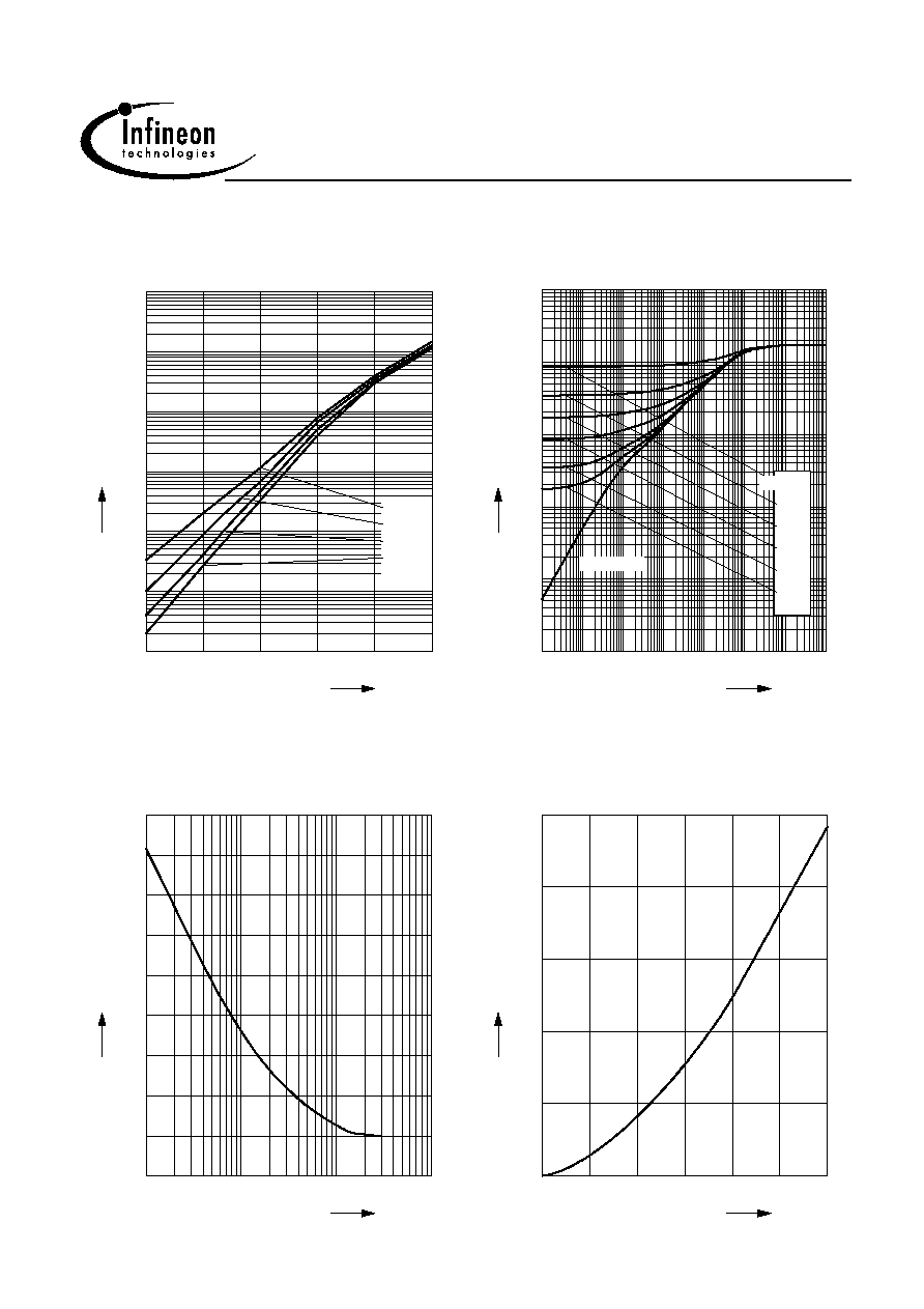
5 Typ. reverse current vs. reverse voltage
(per leg)I
R
=f(V
R
)
50
100
150
200
V
300
V
R
-4
10
-3
10
-2
10
-1
10
0
10
1
10
2
10
µA
I
R
150∞C
125∞C
100∞C
25∞C
6 Transient thermal impedance (per leg)
Z
thJC
= f (t
p
)
parameter : D = t
p
/T
10
-7
10
-6
10
-5
10
-4
10
-3
10
-2
10
0
s
t
p
-4
10
-3
10
-2
10
-1
10
0
10
1
10
K/W
SDP20S30
Z
thJC
single pulse
0.01
0.02
0.05
0.10
0.20
D = 0.50
7 Typ. capacitance vs. reverse voltage
(per leg)C= f(V
R
)
parameter: T
C
= 25 ∞C, f = 1 MHz
10
0
10
1
10
2
10
3
V
V
R
0
50
100
150
200
250
300
350
pF
450
C
8 Typ. C stored energy (per leg)
E
C
=f(V
R
)
0
50
100
150
200
V
300
V
R
0
0.5
1
1.5
µJ
2.5
E
C

2001-09-07
Page 6
SDP20S30
SDB20S30
Preliminary data
9 Typ. capacitive charge vs. current slope
(per leg)Q
c
=f(di
F
/dt
)
parameter: T
j
= 150 ∞C
100 200 300 400 500 600 700 800
A/µs
1000
di
F
/dt
0
2
4
6
8
10
12
14
16
18
nC
22
Q
c
I
F
*0.5
I
F
I
F
*2

2001-09-07
Page 7
SDP20S30
SDB20S30
Preliminary data
P-TO220-3-1
symbol
[mm]
[inch]
min
max
min
max
A
9.70
10.30
0.3819
0.4055
B
14.88
15.95
0.5858
0.6280
C
0.65
0.86
0.0256
0.0339
D
3.55
3.89
0.1398
0.1531
E
2.60
3.00
0.1024
0.1181
F
6.00
6.80
0.2362
0.2677
G
13.00
14.00
0.5118
0.5512
H
4.35
4.75
0.1713
0.1870
K
0.38
0.65
0.0150
0.0256
L
0.95
1.32
0.0374
0.0520
M
N
4.30
4.50
0.1693
0.1772
P
1.17
1.40
0.0461
0.0551
T
2.30
2.72
0.0906
0.1071
2.54 typ.
0.1 typ.
dimensions
P-TO220-3-1
symbol
[mm]
[inch]
min
max
min
max
A
9.80
10.00
0.3858
0.3937
B
C
1.25
1.75
0.0492
0.0689
D
0.95
1.15
0.0374
0.0453
E
F
0.72
0.85
0.0283
0.0335
G
H
4.30
4.50
0.1693
0.1772
K
1.28
1.40
0.0504
0.0551
L
9.00
9.40
0.3543
0.3701
M
2.30
2.50
0.0906
0.0984
N
P
0.00
0.20
0.0000
0.0079
Q
3.30
3.90
0.1299
0.1535
R
S
1.70
2.50
0.0669
0.0984
T
0.50
0.65
0.0197
0.0256
U
V
W
X
Y
Z
9.40 typ.
0.3701 typ.
16.15 typ.
0.6358 typ.
6.43 typ.
0.2532 typ.
4.60 typ.
0.1811 typ.
10.8 typ.
0.4252 typ.
1.35 typ.
0.0532 typ.
14.1 typ.
0.5551 typ.
8∞ max
8∞ max
dimensions
2.54 typ.
0.1 typ.
5.08 typ.
0.2 typ.
1.3 typ.
0.0512 typ.
TO-220-3-45 (P-TO220SMD)

2001-09-07
Page 8
SDP20S30
SDB20S30
Preliminary data
Published by
Infineon Technologies AG,
Bereichs Kommunikation
St.-Martin-Strasse 53,
D-81541 M¸nchen
© Infineon Technologies AG 1999
All Rights Reserved.
Attention please!
The information herein is given to describe certain components and shall not be considered as warranted
characteristics.
Terms of delivery and rights to technical change reserved.
We hereby disclaim any and all warranties, including but not limited to warranties of non-infringement,
regarding circuits, descriptions and charts stated herein.
Infineon Technologies is an approved CECC manufacturer.
Information
For further information on technology, delivery terms and conditions and prices please contact your nearest
Infineon Technologies Office in Germany or our Infineon Technologies Reprensatives worldwide (see address list).
Warnings
Due to technical requirements components may contain dangerous substances.
For information on the types in question please contact your nearest Infineon Technologies Office.
Infineon Technologies Components may only be used in life-support devices or systems with the express
written approval of Infineon Technologies, if a failure of such components can reasonably be expected to
cause the failure of that life-support device or system, or to affect the safety or effectiveness of that device
or system Life support devices or systems are intended to be implanted in the human body, or to support
and/or maintain and sustain and/or protect human life. If they fail, it is reasonable to assume that the health
of the user or other persons may be endangered.