
C o o l S E T TM - F 2
I C E 2 A 0 5 6 5 / 1 6 5 / 2 6 5 / 3 6 5
I C E 2 B 0 5 6 5 / 1 6 5 / 2 6 5 / 3 6 5
I C E 2 A 0 5 6 5 G
I C E 2 A 0 5 6 5 Z
I C E 2 A 1 8 0 Z / 2 8 0 Z
I C E 2 A 7 6 5 I / 2 B 7 6 5 I
I C E 2 A 7 6 5 P 2 / 2 B 7 6 5 P 2
O f f - L i n e S M P S C u r r e n t M o d e
C o n t r o l l e r w i t h i n t e g r a t e d 6 5 0 V /
8 0 0 V C o o l M O S TM
N e v e r s t o p t h i n k i n g .
P o w e r M a n a g e m e n t & S u p p l y
D a t a s h e e t
, V2.0, 11 Jun 2004

Edition 2004-06-11
Published by Infineon Technologies AG,
St.-Martin-Strasse 53,
D-81541 M¸nchen
©
Infineon Technologies AG 1999.
All Rights Reserved.
Attention please!
The information herein is given to describe certain components and shall not be considered as warranted char-
acteristics.
Terms of delivery and rights to technical change reserved.
We hereby disclaim any and all warranties, including but not limited to warranties of non-infringement, regarding
circuits, descriptions and charts stated herein.
Infineon Technologies is an approved CECC manufacturer.
Information
For further information on technology, delivery terms and conditions and prices please contact your nearest
Infineon Technologies Office in Germany or our Infineon Technologies Representatives worldwide (see address
list).
Warnings
Due to technical requirements components may contain dangerous substances. For information on the types in
question please contact your nearest Infineon Technologies Office.
Infineon Technologies Components may only be used in life-support devices or systems with the express written
approval of Infineon Technologies, if a failure of such components can reasonably be expected to cause the failure
of that life-support device or system, or to affect the safety or effectiveness of that device or system. Life support
devices or systems are intended to be implanted in the human body, or to support and/or maintain and sustain
and/or protect human life. If they fail, it is reasonable to assume that the health of the user or other persons may
be endangered.
For questions on technology, delivery and prices please contact the Infineon Technologies Offices in Germany or
the Infineon Technologies Companies and Representatives worldwide: see our webpage at http://
www.infineon.com.
CoolMOSTM, CoolSETTM are trademarks of Infineon Technologies AG.
CoolSETTM-F2
Revision History: 2004-06-11
Datasheet
Previous Version:
Page
Subjects (major changes since last revision)
Version 2.0 3 11 Jun 2004
CoolSETTM-F2
P-TO220-6-46
P-TO220-6-47
P-TO220-6-47
P-TO220-6-46
P-DIP-8-4, -6
P-DIP-7-1
P-DIP-7-1
P-DIP-8-6
P-DSO-16/12
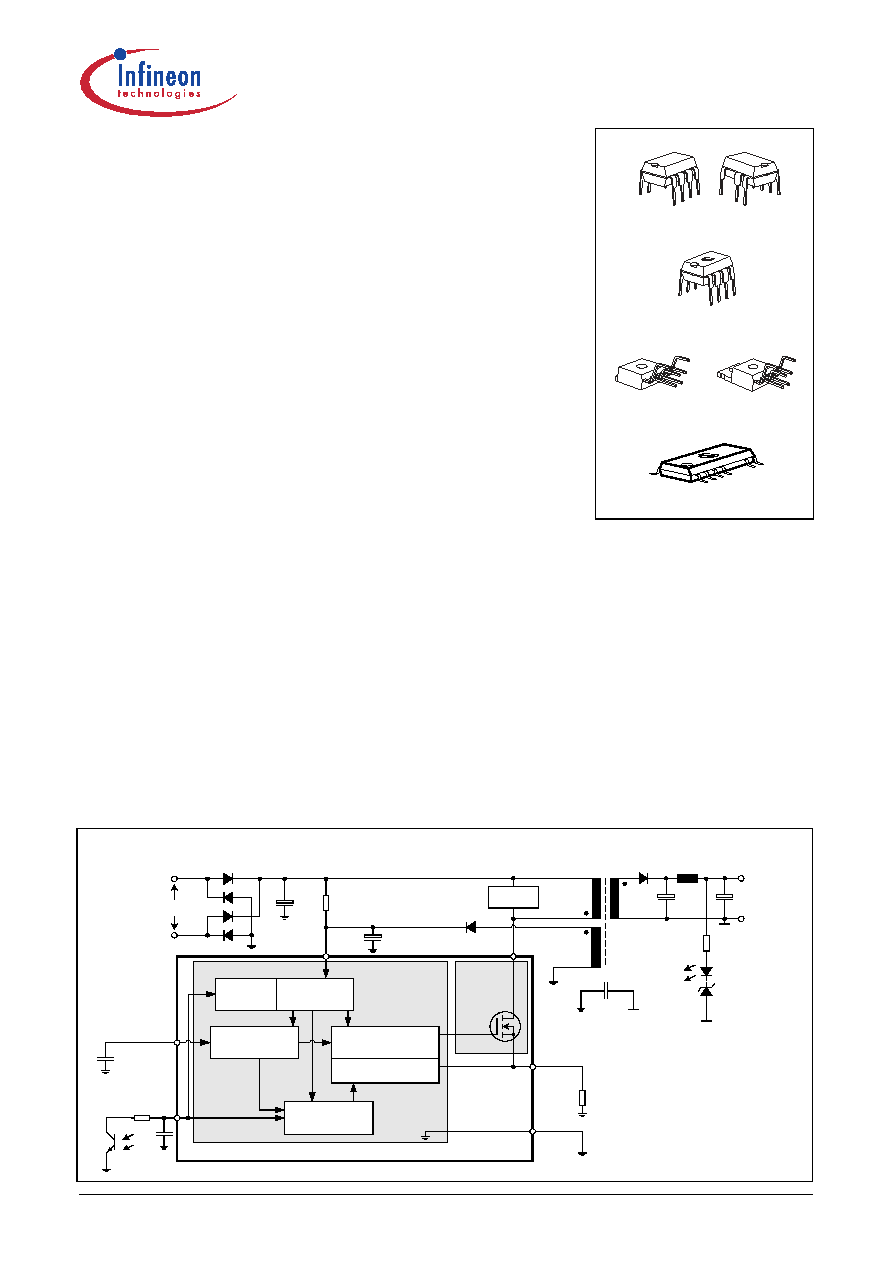
Product Highlights
∑ Best in class in DIP8, DIP7, TO220 and DSO16/12
packages
∑ No heat-sink required for DIP8, DIP7 and DSO16/12
∑ Increased creepage distance for TO220, DIP7 and
DSO16/12
∑ Isolated drain for TO220 packages
∑ Lowest standby power dissipation
∑ Enhanced protection functions with
Auto Restart Mode
C
Soft Start
C
VCC
R
Start-up
VCC
-
Converter
DC Output
+
CoolSETTM-F2
Snubber
Power
Management
Protection Unit
Soft-Start Control
PWM Controller
Current Mode
FB
85 ... 270 VAC
Drain
Feedback
Feedback
Typical Application
CoolMOSTM
PWM-Controller
Low Power
StandBy
Precise Low Tolerance
Peak Current Limitation
R
Sense
Isense
GND
SoftS
Description
The second generation CoolSETTM-F2 provides several
special enhancements to satisfy the needs for low power
standby and protection features. In standby mode
frequency reduction is used to lower the power
consumption and support a stable output voltage in this
mode. The frequency reduction is limited to 20kHz/21.5
kHz to avoid audible noise. In case of failure modes like
open loop, overvoltage or overload due to short circuit the
device switches in Auto Restart Mode which is controlled by
the internal protection unit. By means of the internal precise
peak current limitation, the dimension of the transformer
and the secondary diode can be sized lower which leads to
more cost effective for the overall system.
Off-Line SMPS Current Mode Controller
with integrated 650V/800V CoolMOSTM
Features
∑
650V/800V avalanche rugged CoolMOSTM
∑
Only few external components required
∑
Input Vcc Undervoltage Lockout
∑
67kHz/100kHz switching frequency
∑
Max duty cycle 72%
∑
Low Power Standby Mode to meet
European Commission Requirements
∑
Thermal Shut Down with Auto Restart
∑
Overload and Open Loop Protection
∑
Overvoltage Protection during Auto Restart
∑
Adjustable Peak Current Limitation via
external resistor
∑
Overall tolerance of Current Limiting
< ±5%
∑
Internal Leading Edge Blanking
∑
User defined Soft Start Soft Switching for low EMI

Version 2.0 4 11 Jun 2004
CoolSETTM-F2
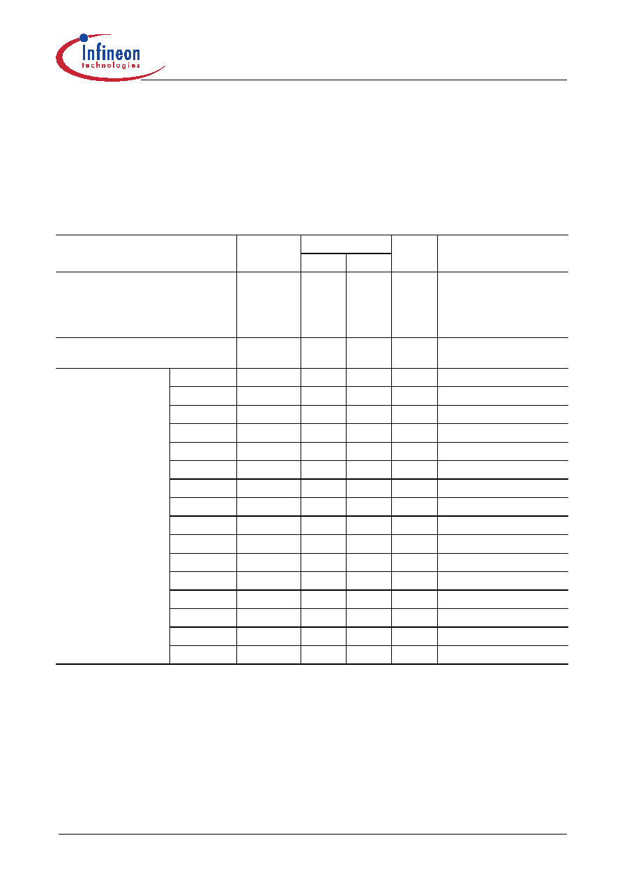
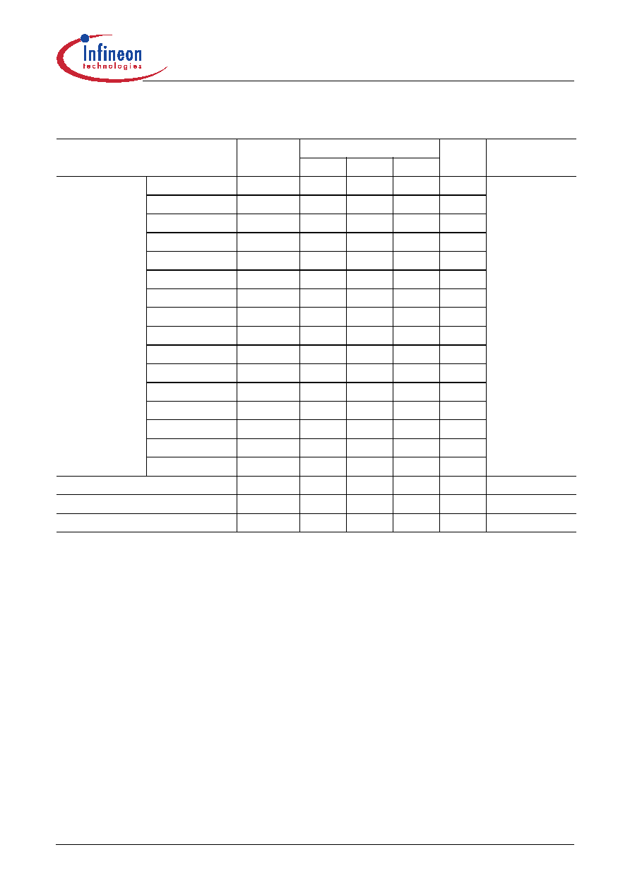
Ordering Codes
Type
Ordering Code
Package
V
DS
F
OSC
R
DSon
1)
1)
typ @ T=25∞C
230VAC ±15%
2)
2)
Maximum power rating at T
a
=75∞C, T
j
=125∞C and with copper area on PCB = 6cm≤
85-265 VAC
2)
ICE2A0565
Q67040-S4542
P-DIP-8-6
650V
100kHz
4.7
23W
13W
ICE2A165
Q67040-S4426
P-DIP-8-6
650V
100kHz
3.0
31W
18W
ICE2A265
Q67040-S4414
P-DIP-8-6
650V
100kHz
0.9
52W
32W
ICE2A365
Q67040-S4415
P-DIP-8-6
650V
100kHz
0.45
67W
45W
ICE2B0565
Q67040-S4540
P-DIP-8-6
650V
67kHz
4.7
23W
13W
ICE2B165
Q67040-S4489
P-DIP-8-6
650V
67kHz
3.0
31W
18W
ICE2B265
Q67040-S4478
P-DIP-8-6
650V
67kHz
0.9
52W
32W
ICE2B365
Q67040-S4490
P-DIP-8-6
650V
67kHz
0.45
67W
45W
ICE2A0565Z
Q67040-S4541
P-DIP-7-1
650V
100kHz
4.7
23W
13W
ICE2A180Z
Q67040-S4546
P-DIP-7-1
800V
100kHz
3.0
29W
17W
ICE2A280Z
Q67040-S4547
P-DIP-7-1
800V
100KHz
0.8
50W
31W
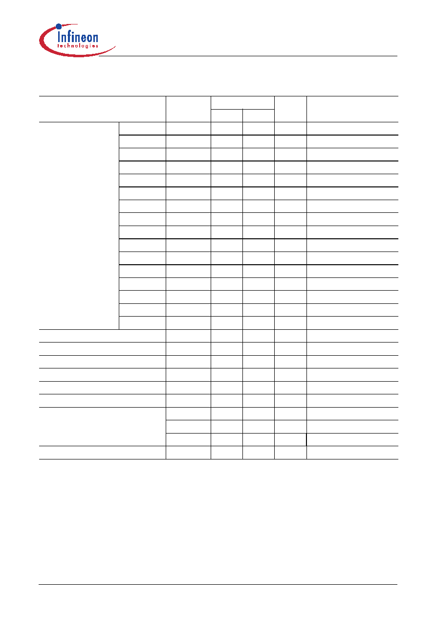
Type
Ordering Code
Package
V
DS
F
OSC
R
DSon
1)
1)
typ @ T=25∞C
230VAC ±15%
2)
2)
Maximum power rating at T
a
=75∞C, T
j
=125∞C and with copper area on PCB = 6cm≤
85-265 VAC
2)
ICE2A0565G
Q67040-S4656
P-DSO-16/12
650V
100kHz
4.7
23W
13W
Type
Ordering Code
Package
V
DS
F
OSC
R
DSon
1)
1)
typ @ T=25∞C
230VAC ±15%
2)
2)
Maximum practical continuous power in an open frame design at T
a
=75∞C, T
j
=125∞C and R
thCA
=2.7K/W
85-265 VAC
2)
ICE2A765I
Q67040-S4609
P-TO-220-6-46
650V
100kHz
0.45
240W
130W
ICE2B765I
Q67040-S4607
P-TO-220-6-46
650V
67kHz
0.45
240W
130W
ICE2A765P2
Q67040-S4610
P-TO-220-6-47
650V
100kHz
0.45
240W
130W
ICE2B765P2
Q67040-S4608
P-TO-220-6-47
650V
67kHz
0.45
240W
130W

CoolSETTM-F2
Table of Contents
Page
Version 2.0 5 11 Jun 2004
1
Pin Configuration and Functionality . . . . . . . . . . . . . . . . . . . . . . . . . . . . .6
1.1
Pin Configuration with P-DIP-8-6 . . . . . . . . . . . . . . . . . . . . . . . . . . . . . . . . . .6
1.2
Pin Configuration with P-DIP-7-1 . . . . . . . . . . . . . . . . . . . . . . . . . . . . . . . . . .6
1.3
Pin Configuration with P-TO220-6-46/47 . . . . . . . . . . . . . . . . . . . . . . . . . . . .7
1.4
Pin Configuration with P-DSO-16/12 . . . . . . . . . . . . . . . . . . . . . . . . . . . . . . .7
1.5
Pin Functionality . . . . . . . . . . . . . . . . . . . . . . . . . . . . . . . . . . . . . . . . . . . . . .8
2
Representative Blockdiagram . . . . . . . . . . . . . . . . . . . . . . . . . . . . . . . . . .9
3
Functional Description . . . . . . . . . . . . . . . . . . . . . . . . . . . . . . . . . . . . . . .10
3.1
Power Management . . . . . . . . . . . . . . . . . . . . . . . . . . . . . . . . . . . . . . . . . . .10
3.2
Improved Current Mode . . . . . . . . . . . . . . . . . . . . . . . . . . . . . . . . . . . . . . . .10
3.2.1
PWM-OP . . . . . . . . . . . . . . . . . . . . . . . . . . . . . . . . . . . . . . . . . . . . . . . . .11
3.2.2
PWM-Comparator . . . . . . . . . . . . . . . . . . . . . . . . . . . . . . . . . . . . . . . . . .11
3.3
Soft-Start . . . . . . . . . . . . . . . . . . . . . . . . . . . . . . . . . . . . . . . . . . . . . . . . . . .12
3.4
Oscillator and Frequency Reduction . . . . . . . . . . . . . . . . . . . . . . . . . . . . . .13
3.4.1
Oscillator . . . . . . . . . . . . . . . . . . . . . . . . . . . . . . . . . . . . . . . . . . . . . . . . .13
3.4.2
Frequency Reduction . . . . . . . . . . . . . . . . . . . . . . . . . . . . . . . . . . . . . . . .13
3.5
Current Limiting . . . . . . . . . . . . . . . . . . . . . . . . . . . . . . . . . . . . . . . . . . . . . .13
3.5.1
Leading Edge Blanking . . . . . . . . . . . . . . . . . . . . . . . . . . . . . . . . . . . . . .13
3.5.2
Propagation Delay Compensation . . . . . . . . . . . . . . . . . . . . . . . . . . . . . .14
3.6
PWM-Latch . . . . . . . . . . . . . . . . . . . . . . . . . . . . . . . . . . . . . . . . . . . . . . . . .14
3.7
Driver . . . . . . . . . . . . . . . . . . . . . . . . . . . . . . . . . . . . . . . . . . . . . . . . . . . . . .14
3.8
Protection Unit (Auto Restart Mode) . . . . . . . . . . . . . . . . . . . . . . . . . . . . . .15
3.8.1
Overload / Open Loop with Normal Load . . . . . . . . . . . . . . . . . . . . . . . .15
3.8.2
Overvoltage due to Open Loop with No Load . . . . . . . . . . . . . . . . . . . . .16
3.8.3
Thermal Shut Down . . . . . . . . . . . . . . . . . . . . . . . . . . . . . . . . . . . . . . . . .16
4
Electrical Characteristics . . . . . . . . . . . . . . . . . . . . . . . . . . . . . . . . . . . . .17
4.1
Absolute Maximum Ratings . . . . . . . . . . . . . . . . . . . . . . . . . . . . . . . . . . . . .17
4.2
Thermal Impedance (ICE2X765I and ICE2X765P2) . . . . . . . . . . . . . . . . . .19
4.3
Operating Range . . . . . . . . . . . . . . . . . . . . . . . . . . . . . . . . . . . . . . . . . . . . .19
4.4
Characteristics . . . . . . . . . . . . . . . . . . . . . . . . . . . . . . . . . . . . . . . . . . . . . . .20
4.4.1
Supply Section . . . . . . . . . . . . . . . . . . . . . . . . . . . . . . . . . . . . . . . . . . . . .20
4.4.2
Internal Voltage Reference . . . . . . . . . . . . . . . . . . . . . . . . . . . . . . . . . . .21
4.4.3
Control Section . . . . . . . . . . . . . . . . . . . . . . . . . . . . . . . . . . . . . . . . . . . .21
4.4.4
Protection Unit . . . . . . . . . . . . . . . . . . . . . . . . . . . . . . . . . . . . . . . . . . . . .22
4.4.5
Current Limiting . . . . . . . . . . . . . . . . . . . . . . . . . . . . . . . . . . . . . . . . . . . .22
4.4.6
CoolMOSTM Section . . . . . . . . . . . . . . . . . . . . . . . . . . . . . . . . . . . . . . . . .23
5
Typical Performance Characteristics . . . . . . . . . . . . . . . . . . . . . . . . . . .25
6
Layout Recommendation for C
18
. . . . . . . . . . . . . . . . . . . . . . . . . . . . . . .31
7
Outline Dimension . . . . . . . . . . . . . . . . . . . . . . . . . . . . . . . . . . . . . . . . . . .32
Version 2.0 6 11 Jun 2004
CoolSETTM-F2
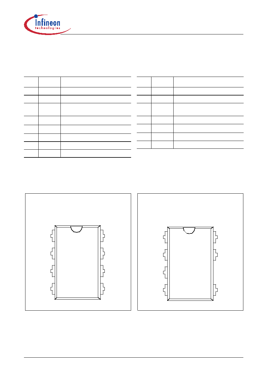
Pin Configuration and Functionality
1
Pin Configuration and Functionality
1.1
Pin Configuration with P-DIP-8-6
Figure 1
Pin Configuration P-DIP-8-6 (top view)
1.2
Pin Configuration with P-DIP-7-1
Figure 2
Pin Configuration P-DIP-7-1 (top view)
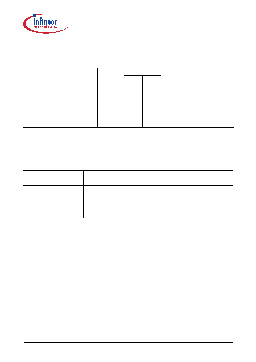
Pin
Symbol
Function
1
SoftS
Soft-Start
2
FB
Feedback
3
Isense
Controller Current Sense Input,
CoolMOSTM Source Output
4
Drain
650V
1)
/800V
2)
CoolMOSTM Drain
1)
at T
j
= 110∞C
5
Drain
650V
1)
/800V
2)
CoolMOSTM Drain
2)
at T
j
= 25∞C
6
N.C
Not connected
7
VCC
Controller Supply Voltage
8
GND
Controller Ground
Package P-DIP-8-6
1
6
7
8
4
3
2
5
VCC
FB
Isense
Drain
SoftS
N.C
GND
Drain
Pin
Symbol
Function
1
SoftS
Soft-Start
2
FB
Feedback
3
Isense
Controller Current Sense Input,
CoolMOSTM Source Output
4
N.C.
Not connected
5
Drain
650V
1)
/800V
2)
CoolMOSTM Drain
1)
at T
j
= 110∞C
2)
at T
j
= 25∞C
7
VCC
Controller Supply Voltage
8
GND
Controller Ground
1
7
8
4
3
2
5
VCC
FB
Isense
n.c.
SoftS
GND
Drain
Package P-DIP-7-1
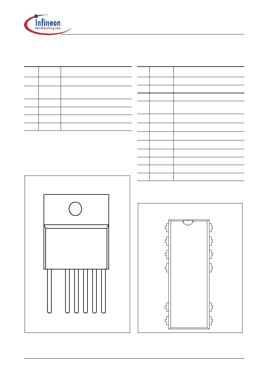
Version 2.0 7 11 Jun 2004
CoolSETTM-F2
Pin Configuration and Functionality
1.3
Pin Configuration with P-TO220-6-46/47
Figure 3
Pin Configuration P-TO220-6-46/47
(top view)
1.4
Pin Configuration with P-DSO-16/12
Figure 4
Pin Configuration P-DSO-16/12 (top view)
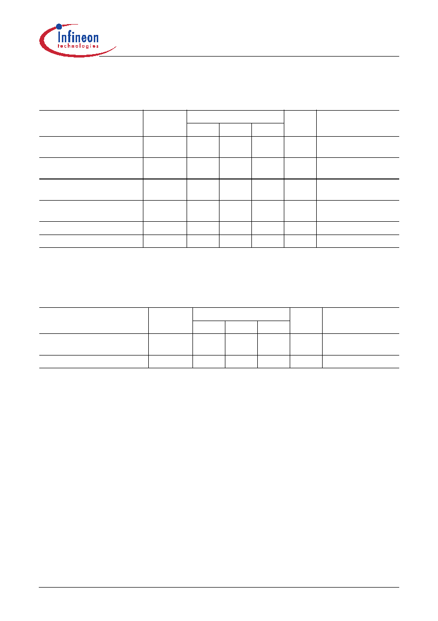
Pin
Symbol
Function
1
Drain
650V
1)
CoolMOSTM Drain
1)
at T
j
= 110∞C
3
Isense
Controller Current Sense Input,
CoolMOSTM Source Output
4
GND
Controller Ground
5
VCC
Controller Supply Voltage
6
SoftS
Soft-Start
7
FB
Feedback
Package P-TO220-6-46/47
1
Dr
ai
n
2
3
4
5
6
7
Is
ens
e
GN
D
VC
C
S
o
ftS
FB
Pin
Symbol
Function
1
N.C.
Not Connected
2
SoftS
Soft-Start
3
FB
Feedback
4
Isense
Controller Current Sense Input,
CoolMOSTM Source Output
5
Drain
650V
1)
CoolMOSTM Drain
1)
at T
j
= 110∞C
6
Drain
650V
1)
CoolMOSTM Drain
7
Drain
650V
1)
CoolMOSTM Drain
8
Drain
650V
1)
CoolMOSTM Drain
9
N.C.
Not Connected
10
N.C.
Not Connected
11
VCC
Controller Supply Voltage
12
GND
Controller Ground
Package P-DSO-16/12
10
11
12
9
VCC
SoftS
FB
Isense
N.C
N.C.
G N D
N .C .
Drain
Drain
8
7
3
2
1
4
D rain
D rain
5
6

Version 2.0 8 11 Jun 2004
CoolSETTM-F2
Pin Configuration and Functionality
1.5
Pin Functionality
SoftS (Soft Start & Auto Restart Control)
This pin combines the function of Soft Start in case of
Start Up and Auto Restart Mode and the controlling of
the Auto Restart Mode in case of an error detection.
FB (Feedback)
The information about the regulation is provided by the
FB Pin to the internal Protection Unit and to the internal
PWM-Comparator to control the duty cycle.
Isense (Current Sense)
The Current Sense pin senses the voltage developed
on the series resistor inserted in the source of the
integrated CoolMOSTM. When Isense reaches the
internal threshold of the Current Limit Comparator, the
Driver output is disabled. By this means the Over
Current Detection is realized.
Furthermore the current information is provided for the
PWM-Comparator to realize the Current Mode.
Drain (Drain of integrated CoolMOSTM)
Pin Drain is the connection to the Drain of the internal
CoolMOS
TM
.
VCC (Power supply)
This pin is the positive supply of the IC. The operating
range is between 8.5V and 21V.
To provide overvoltage protection the driver gets
disabled when the voltage becomes higher than 16.5V
during Start Up Phase.
GND (Ground)
This pin is the ground of the primary side of the SMPS.

Version 2.0 9 11 Jun 2004
CoolSETTM-F2
Representative Blockdiagram
2
Representative Blockdiagram
Figure 5
Representative Blockdiagram
Th
ermal
Shutdo
wn
T
j
>
140∞C
Inter
nal Bias
Vol
tage
Refe
rence
6.5V
4.8V
Lead
ing Ed
ge
Bl
anki
ng
220n
s
Und
ervolt
age
Lockout
Osci
ll
ator
Du
t
y
Cy
c
l
e
max
Cur
rent
-Li
mit
Comp
arator
x3.65
Soft-
Start
Comp
arator
Cur
r
e
nt
Li
mi
t
i
ng
PWM OP
I
m
pr
ov
ed C
u
r
ren
t
M
o
d
e
So
f
t
Start
13.5V
8.5V
6.5V
C2
C1
16.5V
4.0V
R
FB
6.5V
Pr
otection
Unit
P
o
w
e
r-
Do
w
n
Reset
P
o
w
e
r-
Up
Reset
Powe
r Manage
m
e
nt
C
S
o
ft
-S
tar
t
C
VC
C
R
St
ar
t
-
u
p
85 ...
270 VAC
C
Line
VCC
GN
D
+
-
Con
ver
ter
DC
O
ut
put
V
OU
T
f
s
t
an
dby
-f
nor
m
Co
olSE
TTM-F2
Opto
coupler
Snubbe
r
Spik
e
Bl
anki
ng
5
s
PWM
Comp
arator
R
SQ
Q
Err
or-
Latch
C4
5.3V
C3
4.8V
R
S
o
ft
-S
tar
t
Gate
Dr
iv
er
G3
G2
G1
G4
SoftS
5.3V
T1
V
cs
th
Prop
agati
on-D
elay
Comp
ensation
R
S
Q
Q
PWM-La
tch
0.72
Cl
o
c
k
U
FB
f
os
c
f
nor
m
f
s
t
an
dby
Stan
db
y Un
it
FB
4.0V
R
S
ens
e
Drain
Isense
0.8V
C5
0.3V
10k
D1
5.6V
Co
olMOS
TM
IC
E
2
A
x
x
x
x
IC
E
2
B
x
x
x
x
f
norm
f
standby
10
0k
Hz
21
.
5k
H
z
67
kH
z
20
kH
z
Du
ty Cyc
l
e
Max

Version 2.0 10 11 Jun 2004
CoolSETTM-F2
Functional Description
3
Functional Description
3.1
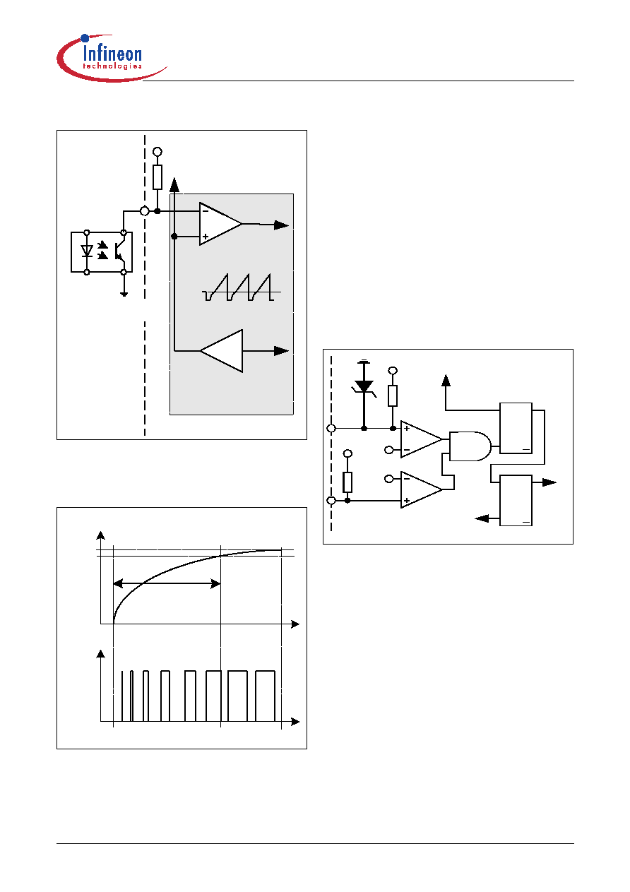
Power Management
Figure 6
Power Management
The Undervoltage Lockout monitors the external
supply voltage V
VCC
. In case the IC is inactive the
current consumption is max. 55µA. When the SMPS is
plugged to the main line the current through R
Start-up
charges the external Capacitor C
VCC
. When V
VCC
exceeds the on-threshold V
CCon
=13.5V the internal bias
circuit and the voltage reference are switched on. After
that the internal bandgap generates a reference
voltage V
REF
=6.5V to supply the internal circuits. To
avoid uncontrolled ringing at switch-on a hysteresis is
implemented which means that switch-off is only after
active mode when Vcc falls below 8.5V.
In case of switch-on a Power Up Reset is done by
resetting the internal error-latch in the protection unit.
When V
VCC
falls below the off-threshold V
CCoff
=8.5V the
internal reference is switched off and the Power Down
reset let T1 discharging the soft-start capacitor C
Soft-Start
at pin SoftS. Thus it is ensured that at every switch-on
the voltage ramp at pin SoftS starts at zero.
3.2
Improved Current Mode
Figure 7
Current Mode
Current Mode means that the duty cycle is controlled
by the slope of the primary current. This is done by
comparison the FB signal with the amplified current
sense signal.
Figure 8
Pulse Width Modulation
In case the amplified current sense signal exceeds the
FB signal the on-time T
on
of the driver is finished by
resetting the PWM-Latch (see Figure 8).
The primary current is sensed by the external series
resistor R
Sense
inserted in the source of the integrated
CoolMOSTM. By means of Current Mode regulation, the
In te rn a l
B ia s
V o lta g e
R e fe re n c e
6 .5 V
4 .8 V
U n d e rvo lta g e
L o ck o u t
1 3 .5 V
8 .5 V
P o w e r-D o w n
R e se t
P o w e r-U p
R e se t
Po w er M anagem ent
5 .3 V
4 .0 V
T 1
P W M -L a tc h
R
S
Q
Q
E rro r-L a tch
S o ftS
6 .5 V
E rro r-D e te ctio n
V C C
M a in L in e (1 0 0 V -3 8 0 V )
P rim a ry W in d in g
S o ft-S ta rt C o m p a ra to r
C
V C C
R
S oft-S tart
R
S tart-U p
C
S oft-S tart
x3 .6 5
P W M O P
Im proved
C urrent M ode
0 .8 V
P W M C o m p a ra to r
P W M -L a tch
Ise n se
F B
R
S
Q
Q
D rive r
S o ft-S ta rt C o m p a ra to r
t
FB
Amplified Current Signal
T
on
t
0.8V
Driver
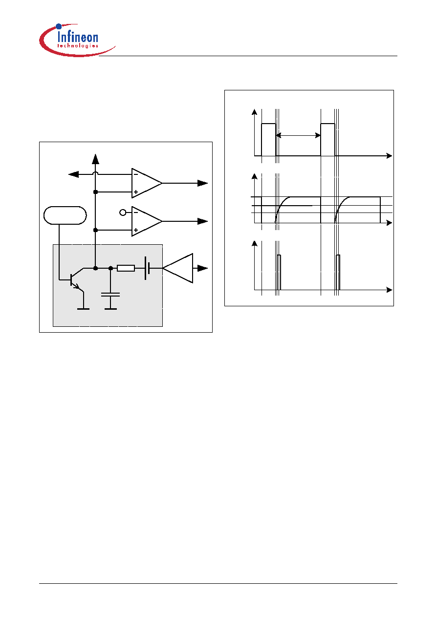
Version 2.0 11 11 Jun 2004
CoolSETTM-F2
Functional Description
secondary output voltage is insensitive on line
variations. Line variation changes the current
waveform slope which controls the duty cycle.
The external R
Sense
allows an individual adjustment of
the maximum source current of the integrated
CoolMOSTM.
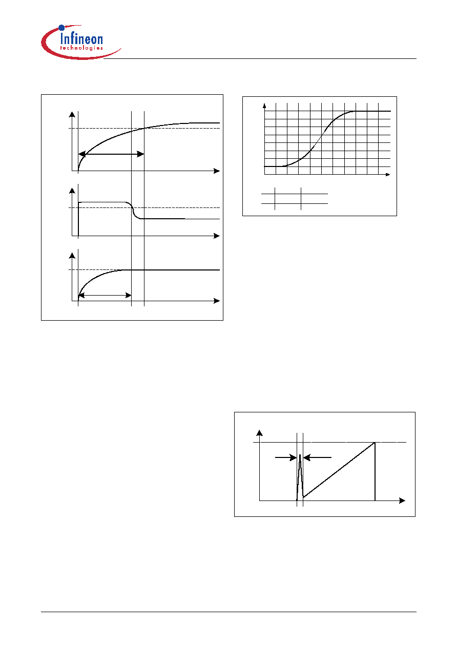
Figure 9
Improved Current Mode
To improve the Current Mode during light load
conditions the amplified current ramp of the PWM-OP
is superimposed on a voltage ramp, which is built by
the switch T
2
, the voltage source V
1
and the 1st order
low pass filter composed of R
1
and C
1
(see Figure 9,
Figure 10). Every time the oscillator shuts down for
max. duty cycle limitation the switch T2 is closed by
V
OSC
. When the oscillator triggers the Gate Driver T2 is
opened so that the voltage ramp can start.
In case of light load the amplified current ramp is to
small to ensure a stable regulation. In that case the
Voltage Ramp is a well defined signal for the
comparison with the FB-signal. The duty cycle is then
controlled by the slope of the Voltage Ramp.
By means of the Comparator C5, the Gate Driver is
switched-off until the voltage ramp exceeds 0.3V. It
allows the duty cycle to be reduced continuously till 0%
by decreasing V
FB
below that threshold.
Figure 10
Light Load Conditions
3.2.1
PWM-OP
The input of the PWM-OP is applied over the internal
leading edge blanking to the external sense resistor
R
Sense
connected to pin Isense. R
Sense
converts the
source current into a sense voltage. The sense voltage
is amplified with a gain of 3.65 by PWM OP. The output
of the PWM-OP is connected to the voltage source V1.
The voltage ramp with the superimposed amplified
current signal is fed into the positive inputs of the PWM-
Comparator, C5 and the Soft-Start-Comparator.
3.2.2
PWM-Comparator
The PWM-Comparator compares the sensed current
signal of the integrated CoolMOS
TM
with the feedback
signal V
FB
(see Figure 11). V
FB
is created by an
external optocoupler or external transistor in
combination with the internal pull-up resistor R
FB
and
provides the load information of the feedback circuitry.
When the amplified current signal of the integrated
CoolMOSTM exceeds the signal V
FB
the PWM-
Comparator switches off the Gate Driver.
x 3 .6 5
P W M O P
0.8V
1 0 k
O sc illa to r
P W M C o m p a ra to r
2 0 p F
T
2
R
1
C
1
F B
P W M -L a tc h
V
1
C 5
0 .3 V
G a te D rive r
V oltage R am p
V
O S C
S o ft-S ta rt C o m p a ra to r
t
t
V
OSC
0.8V
FB
t
max.
Duty Cycle
0.3V
Gate Driver
Voltage Ramp
Version 2.0 12 11 Jun 2004
CoolSETTM-F2
Functional Description
Figure 11
PWM Controlling
3.3
Soft-Start
Figure 12
Soft-Start Phase
The Soft-Start is realized by the internal pull-up resistor
R
Soft-Start
and the external Capacitor C
Soft-Start
(see
Figure 5). The Soft-Start voltage V
SoftS
is generated by
charging the external capacitor C
Soft-Start
by the internal
pull-up resistor R
Soft-Start
. The Soft-Start-Comparator
compares the voltage at pin SoftS at the negative input
with the ramp signal of the PWM-OP at the positive
input. When Soft-Start voltage V
SoftS
is less than
Feedback voltage V
FB
the Soft-Start-Comparator limits
the pulse width by resetting the PWM-Latch (see
Figure 12). In addition to Start-Up, Soft-Start is also
activated at each restart attempt during Auto Restart.
By means of the above mentioned C
Soft-Start
the Soft-
Start can be defined by the user. The Soft-Start is
finished when V
SoftS
exceeds 5.3V. At that time the
Protection Unit is activated by Comparator C4 and
senses the FB by Comparator C3 wether the voltage is
below 4.8V which means that the voltage on the
secondary side of the SMPS is settled. The internal
Zener Diode at SoftS has a clamp voltage of 5.6V to
prevent the internal circuit from saturation (see Figure
13).
Figure 13
Activation of Protection Unit
The Start-Up time T
Start-Up
within the converter output
voltage V
OUT
is settled must be shorter than the Soft-
Start Phase T
Soft-Start
(see Figure 14).
By means of Soft-Start there is an effective
minimization of current and voltage stresses on the
integrated CoolMOSTM, the clamp circuit and the output
overshoot and prevents saturation of the transformer
during Start-Up.
x3 .6 5
P W M O P
Im proved
C urrent M ode
P W M C o m p a ra to r
Ise n se
S o ft-S ta rt C o m p a ra to r
6 .5 V
P W M -L a tch
0 .8 V
F B
O p to co u p le r
R
F B
t
5 .3 V
V
S o ftS
G a te D rive r
t
T
S o ft-S ta rt
5 .6 V
6 .5 V
R
F B
6 .5 V
P o w e r-U p R e s e t
C 4
5 .3 V
C 3
4 .8 V
R
S o ft-S ta rt
F B
R
S
Q
Q
E rro r-L a tc h
R
S
Q
Q
P W M -L a tc h
G 2
C lo c k
G a te
D riv e r
5 .6 V
S o ftS
C
Soft
Start
≠
T
Soft
Start
≠
R
Soft
Start
≠
1.69
◊
--------------------------------------
=
Version 2.0 13 11 Jun 2004
CoolSETTM-F2
Functional Description
Figure 14
Start Up Phase
3.4
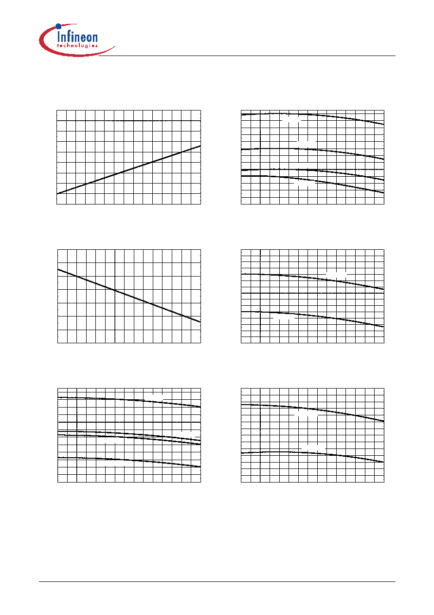
Oscillator and Frequency
Reduction
3.4.1
Oscillator
The oscillator generates a frequency f
switch
= 67kHz/
100kHz. A resistor, a capacitor and a current source
and current sink which determine the frequency are
integrated. The charging and discharging current of the
implemented oscillator capacitor are internally
trimmed, in order to achieve a very accurate switching
frequency. The ratio of controlled charge to discharge
current is adjusted to reach a max. duty cycle limitation
of D
max
=0.72.
3.4.2
Frequency Reduction
The frequency of the oscillator is depending on the
voltage at pin FB. The dependence is shown in Figure
15. This feature allows a power supply to operate at
lower frequency at light loads thus lowering the
switching losses while maintaining good cross
regulation performance and low output ripple. In case
of low power the power consumption of the whole
SMPS can now be reduced very effective. The minimal
reachable frequency is limited to 20kHz/21.5 kHz to
avoid audible noise in any case.
Figure 15
Frequency Dependence
3.5
Current Limiting
There is a cycle by cycle current limiting realized by the
Current-Limit Comparator to provide an overcurrent
detection. The source current of the integrated
CoolMOS
TM
is sensed via an external sense resistor
R
Sense
. By means of R
Sense
the source current is
transformed to a sense voltage V
Sense
. When the
voltage V
Sense
exceeds the internal threshold voltage
V
csth
the Current-Limit-Comparator immediately turns
off the gate drive. To prevent the Current Limiting from
distortions caused by leading edge spikes a Leading
Edge Blanking is integrated at the Current Sense.
Furthermore a Propagation Delay Compensation is
added to support the immediate shut down of the
CoolMOSTM in case of overcurrent.
3.5.1
Leading Edge Blanking
Figure 16
Leading Edge Blanking
Each time when CoolMOSTM is switched on a leading
spike is generated due to the primary-side
capacitances and secondary-side rectifier reverse
recovery time. To avoid a premature termination of the
switching pulse this spike is blanked out with a time
constant of t
LEB
= 220ns. During that time the output of
t
t
V
S o ftS
t
5 .3 V
4 .8 V
T
S o ft-S ta rt
V
O U T
V
F B
V
O U T
T
S ta rt-U p
67kHz
100kHz
20kHz
21.5kHz
21.5
65
100
1.0
1.1
1.2
1.3
1.4
1.5
1.6
1.7
1.8
1.9
2.0
kHz
V
FB
V
f
OS
C
ICE2Bxxxx
ICE2Axxxx
f
norm
f
standby
t
V
S en s e
V
cs th
t
L E B
= 2 2 0 n s
Version 2.0 14 11 Jun 2004
CoolSETTM-F2
Functional Description
the Current-Limit Comparator cannot switch off the
gate drive.
3.5.2
Propagation Delay Compensation
In case of overcurrent detection by I
Limit
the shut down
of CoolMOSTM is delayed due to the propagation delay
of the circuit. This delay causes an overshoot of the
peak current I
peak
which depends on the ratio of dI/dt of
the peak current (see Figure 17).
.
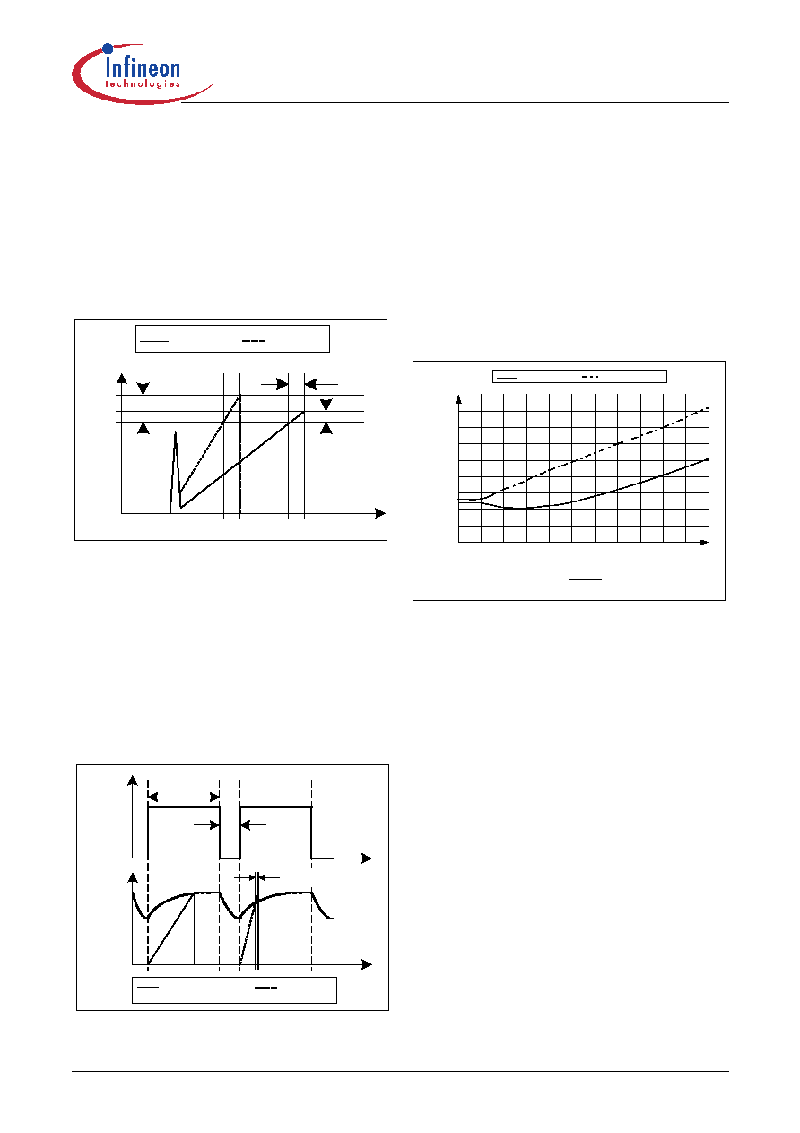
Figure 17
Current Limiting
The overshoot of Signal2 is bigger than of Signal1 due
to the steeper rising waveform.
A propagation delay compensation is integrated to
bound the overshoot dependent on dI/dt of the rising
primary current. That means the propagation delay
time between exceeding the current sense threshold
V
csth
and the switch off of CoolMOSTM is compensated
over temperature within a range of at least.
Figure 18
Dynamic Voltage Threshold V
csth
The propagation delay compensation is done by
means of a dynamic threshold voltage V
csth
(see Figure
18). In case of a steeper slope the switch off of the
driver is earlier to compensate the delay.
E.g. I
peak
= 0.5A with R
Sense
= 2. Without propagation
delay compensation the current sense threshold is set
to a static voltage level V
csth
=1V. A current ramp of
dI/dt = 0.4A/µs, that means dV
Sense
/dt = 0.8V/µs, and a
propagation delay time of i.e. t
Propagation Delay
=180ns
leads then to a I
peak
overshoot of 12%. By means of
propagation delay compensation the overshoot is only
about 2% (see Figure 19).
Figure 19
Overcurrent Shutdown
3.6
PWM-Latch
The oscillator clock output applies a set pulse to the
PWM-Latch when initiating CoolMOSTM conduction.
After setting the PWM-Latch can be reset by the PWM-
OP, the Soft-Start-Comparator, the Current-Limit-
Comparator, Comparator C3 or the Error-Latch of the
Protection Unit. In case of resetting the driver is shut
down immediately.
3.7
Driver
The driver-stage drives the gate of the CoolMOSTM and
is optimized to minimize EMI and to provide high circuit
efficiency. This is done by reducing the switch on slope
when reaching the CoolMOSTM threshold. This is
achieved by a slope control of the rising edge at the
driver's output (see Figure 20) to the CoolMOSTM gate.
Thus the leading switch on spike is minimized. When
CoolMOSTM is switched off, the falling shape of the
driver is slowed down when reaching 2V to prevent an
overshoot below ground. Furthermore the driver circuit
is designed to eliminate cross conduction of the output
stage. At voltages below the undervoltage lockout
threshold V
VCCoff
the gate drive is active low.
t
I
Sense
I
Limit
t
Propagation Delay
I
Overshoot1
I
peak1
Signal2
Signal1
I
Overshoot2
I
peak2
0 R
Sense
dI
peak
dt
------------
◊
dV
Sense
dt
---------------
t
V
csth
V
OSC
Signal1
Signal2
V
Sense
max. Duty Cycle
off time
t
Propagation Delay
0.9
0.95
1
1.05
1.1
1.15
1.2
1.25
1.3
0
0.2
0.4
0.6
0.8
1
1.2
1.4
1.6
1.8
2
with compensation
without compensation
dt
dV
Sense
V
V/us
V
Se
n
s
e
Version 2.0 15 11 Jun 2004
CoolSETTM-F2
Functional Description
Figure 20
Internal Gate Rising Slope
3.8
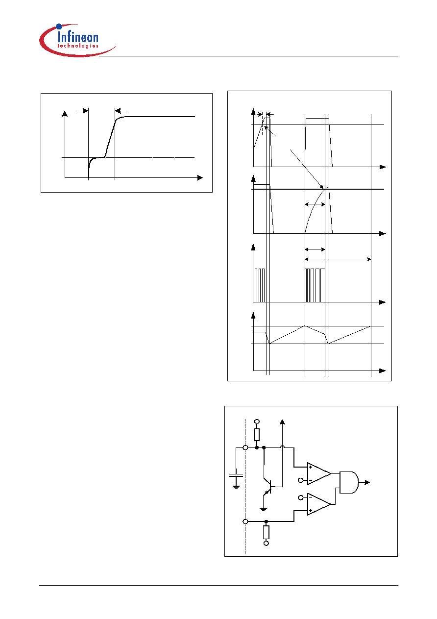
Protection Unit (Auto Restart Mode)
An overload, open loop and overvoltage detection is
integrated within the Protection Unit. These three
failure modes are latched by an Error-Latch. Additional
thermal shutdown is latched by the Error-Latch. In case
of those failure modes the Error-Latch is set after a
blanking time of 5µs and the CoolMOSTM is shut down.
That blanking prevents the Error-Latch from distortions
caused by spikes during operation mode.
3.8.1
Overload / Open Loop with Normal
Load
Figure 21 shows the Auto Restart Mode in case of
overload or open loop with normal load. The detection
of open loop or overload is provided by the Comparator
C3, C4 and the AND-gate G2 (see Figure 22). The
detection is activated by C4 when the voltage at pin
SoftS exceeds 5.3V. Till this time the IC operates in the
Soft-Start Phase. After this phase the comparator C3
can set the Error-Latch in case of open loop or overload
which leads the feedback voltage V
FB
to exceed the
threshold of 4.8V. After latching VCC decreases till
8.5V and inactivates the IC. At this time the external
Soft-Start capacitor is discharged by the internal
transistor T1 due to Power Down Reset. When the IC
is inactive V
VCC
increases till V
CCon
= 13.5V by charging
the Capacitor C
VCC
by means of the Start-Up Resistor
R
Start-Up
. Then the Error-Latch is reset by Power Up
Reset and the external Soft-Start capacitor C
Soft-Start
is
charged by the internal pull-up resistor R
Soft-Start
. During
the Soft-Start Phase which ends when the voltage at
pin SoftS exceeds 5.3V the detection of overload and
open loop by C3 and G2 is inactive. In this way the Start
Up Phase is not detected as an overload.
Figure 21
Auto Restart Mode
Figure 22
FB-Detection
t
V
G a te
5 V
c a . t = 1 3 0 n s
Overload / Open Loop with Normal Load
FB
t
4.8V
5.3V
SoftS
5µs Blanking
Failure
Detection
Soft-Start Phase
VCC
13.5V
8.5V
t
Driver
t
T
Restart
T
Burst1
t
R
S o ft-S ta rt
6 .5 V
C
S o ft-S ta rt
C 4
5 .3 V
C 3
4 .8 V
G 2
T 1
E rro r-L a tc h
P o w e r U p R e se t
R
F B
6 .5 V
F B
S o ftS

Version 2.0 16 11 Jun 2004
CoolSETTM-F2
Functional Description
But the Soft-Start Phase must be finished within the
Start Up Phase to force the voltage at pin FB below the
failure detection threshold of 4.8V.
3.8.2
Overvoltage due to Open Loop with
No Load
Figure 23
Auto Restart Mode
Figure 23 shows the Auto Restart Mode for open loop
and no load condition. In case of this failure mode the
converter output voltage increases and also VCC. An
additional protection by the comparators C1, C2 and
the AND-gate G1 is implemented to consider this
failure mode (see Figure 24).The overvoltage detection
is provided by Comparator C1 only in the first time
during the Soft-Start Phase till the Soft-Start voltage
exceeds the threshold of the Comparator C2 at 4.0V
and the voltage at pin FB is above 4.8V. When VCC
exceeds 16.5V during the overvoltage detection phase
C1 can set the Error-Latch and the Burst Phase during
Auto Restart Mode is finished earlier. In that case
T
Burst2
is shorter than T
Soft-Start
. By means of C2 the
normal operation mode is prevented from overvoltage
detection due to varying of VCC concerning the
regulation of the converter output. When the voltage
V
SoftS
is above 4.0V the overvoltage detection by C1 is
deactivated.
Figure 24
Overvoltage Detection
3.8.3
Thermal Shut Down
Thermal Shut Down is latched by the Error-Latch when
junction temperature T
j
of the pwm controller is
exceeding an internal threshold of 140∞C. In that case
the IC switches in Auto Restart Mode.
Note:
All the values which are mentioned in the
functional description are typical. Please refer
to Electrical Characteristics for min/max limit
values.
O pen loop & no load condition
t
D rive r
1 3 .5 V
1 6 .5 V
F B
4 .8 V
5 µ s B la n k in g
F a ilu re
D e te ctio n
5 .3 V
S o ftS
4 .0 V
O v e rv o lta g e
D e te c tio n P h a s e
S o ft-S ta rt P h a s e
t
t
T
R e s ta rt
T
B u rs t2
V C C
8 .5 V
O v e rv o lta g e D e te ctio n
t
6 .5 V
C
S o ft-S ta rt
V C C
R
S o ft-S ta rt
C 1
1 6 .5 V
C 2
4 .0 V
T 1
S o ftS
G 1
E rro r L a tc h
P o w e r U p R e se t
Version 2.0 17 11 Jun 2004
CoolSETTM-F2
Electrical Characteristics
4
Electrical Characteristics
4.1
Absolute Maximum Ratings
Note:
Absolute maximum ratings are defined as ratings, which when being exceeded may lead to destruction
of the integrated circuit. For the same reason make sure, that any capacitor that will be connected to pin 6
(
V
CC) is discharged before assembling the application circuit.
Parameter
Symbol
Limit Values
Unit
Remarks
min.
max.
Drain Source Voltage
ICE2A0565/165/265/365/765I/765P2
ICE2B0565/165/265/365/765I/765P2
ICE2A0565G
ICE2A0565Z
V
DS
-
650
V
T
j
= 110∞C
Drain Source Voltage
ICE2A180Z/280Z
V
DS
-
800
V
T
j
= 25∞C
Avalanche energy,
repetitive
t
AR
limited by
max.
T
j
=150∞C
1)
1)
Repetitive avalanche causes additional power losses that can be calculated as
P
AV
=
E
AR
*
f
ICE2A0565
E
AR1
-
0.01
mJ
ICE2A165
E
AR2
-
0.07
mJ
ICE2A265
E
AR3
-
0.40
mJ
ICE2A365
E
AR4
-
0.50
mJ
ICE2B0565
E
AR5
-
0.01
mJ
ICE2B165
E
AR6
-
0.07
mJ
ICE2B265
E
AR7
-
0.40
mJ
ICE2B365
E
AR8
-
0.50
mJ
ICE2A0565G
E
AR9
-
0.01
mJ
ICE2A0565Z
E
AR10
-
0.01
mJ
ICE2A180Z
E
AR11
-
0.07
mJ
ICE2A280Z
E
AR12
-
0.40
mJ
ICE2A765I
E
AR13
-
0.50
mJ
ICE2B765I
E
AR14
-
0.50
mJ
ICE2A765P2
E
AR15
-
0.50
mJ
ICE2B765P2
E
AR16
-
0.50
mJ
CoolSETTM-F2
Electrical Characteristics
Version 2.0 18 11 Jun 2004
Parameter
Symbol
Limit Values
Unit
Remarks
min.
max.
Avalanche current,
repetitive tAR limited by
max.
T
j
=150∞C
ICE2A0565
I
AR1
-
0.5
A
ICE2A165
I
AR2
-
1
A
ICE2A265
I
AR3
-
2
A
ICE2A365
I
AR4
-
3
A
ICE2B0565
I
AR5
-
0.5
A
ICE2B165
I
AR6
-
1
A
ICE2B265
I
AR7
-
2
A
ICE2B365
I
AR8
-
3
A
ICE2A0565G
I
AR9
-
0.5
A
ICE2A0565Z
I
AR10
-
0.5
A
ICE2A180Z
I
AR11
-
1
A
ICE2A280Z
I
AR12
-
2
A
ICE2A765I
I
AR13
-
7
A
ICE2B765I
I
AR14
-
7
A
ICE2A765P2
I
AR15
-
7
A
ICE2B765P2
I
AR16
-
7
A
V
CC
Supply Voltage
V
CC
-0.3
22
V
FB Voltage
V
FB
-0.3
6.5
V
SoftS Voltage
V
SoftS
-0.3
6.5
V
I
Sense
I
Sense
-0.3
3
V
Junction Temperature
T
j
-40
150
∞ C
Controller & CoolMOSTM
Storage Temperature
T
S
-50
150
∞ C
Thermal Resistance
Junction-Ambient
R
thJA1
-
90
K/W
P-DIP-8-6
R
thJA2
-
96
K/W
P-DIP-7-1
R
thJA3
-
110
K/W
P-DSO-16/12
ESD Robustness
1)
1)
Equivalent to discharging a 100pF capacitor through a 1.5 k
series resistor
2)
1kV at pin drain of ICE2x0565, ICE2A0565Z and ICE2A0565G
V
ESD
-
2
2)
kV
Human Body Model
Version 2.0 19 11 Jun 2004
CoolSETTM-F2
Electrical Characteristics
4.2
Thermal Impedance (ICE2X765I and ICE2X765P2)
4.3
Operating Range
Note:
Within the operating range the IC operates as described in the functional description.
Parameter
Symbol
Limit Values
Unit
Remarks
min.
max.
Thermal Resistance
Junction-Ambient
ICE2A765I
ICE2B765I
ICE2A765P2
ICE2B765P2
R
thJA4
-
74
K/W
Free standing with no
heat-sink
Junction-Case
ICE2A765I
ICE2B765I
ICE2A765P2
ICE2B765P2
R
thJC
-
2.5
K/W
Parameter
Symbol
Limit Values
Unit
Remarks
min.
max.
V
CC
Supply Voltage
V
CC
V
CCoff
21
V
Junction Temperature of
Controller
T
JCon
-25
130
∞ C
Limited due to thermal shut down
of controller
Junction Temperature of
CoolMOSTM
T
JCoolMOS
-25
150
∞ C

CoolSETTM-F2
Electrical Characteristics
Version 2.0 20 11 Jun 2004
4.4
Characteristics
Note:
The electrical characteristics involve the spread of values given within the specified supply voltage and
junction temperature range
T
J
from ≠ 25
∞
C to 125
∞
C.Typical values represent the median values, which
are related to 25∞C. If not otherwise stated, a supply voltage of
V
CC
= 15 V is assumed.
4.4.1
Supply Section
Parameter
Symbol
Limit Values
Unit
Test Condition
min.
typ.
max.
Start Up Current
I
VCC1
-
27
55
µA
V
CC
=
V
CCon
-0.1V
Supply Current with Inactive
Gate
I
VCC2
-
5.0
6.6
mA
V
SoftS
= 0
I
FB
= 0
Supply Current
with Active Gate
ICE2A0565
I
VCC3
-
5.3
6.7
mA
V
SoftS
= 5V
I
FB
= 0
ICE2A165
I
VCC4
-
6.5
7.8
mA
ICE2A265
I
VCC5
-
6.7
8.0
mA
ICE2A365
I
VCC6
-
8.5
9.8
mA
ICE2B0565
I
VCC7
-
5.2
6.7
mA
ICE2B165
I
VCC8
-
5.5
7.0
mA
ICE2B265
I
VCC9
-
6.1
7.3
mA
ICE2B365
I
VCC10
-
7.1
8.3
mA
ICE2A0565G
I
VCC11
-
5.3
6.7
mA
ICE2A0565Z
I
VCC12
-
5.3
6.7
mA
ICE2A180Z
I
VCC13
-
6.5
7.8
mA
ICE2A280Z
I
VCC14
-
7.7
9.0
mA
Supply Current
with Active Gate
ICE2A765I
I
VCC15
-
8.5
9.8
mA
V
SoftS
= 5V
I
FB
= 0
ICE2B765I
I
VCC16
-
7.1
8.3
mA
ICE2A765P2
I
VCC17
-
8.5
9.8
mA
ICE2B765P2
I
VCC18
-
7.1
8.3
mA
VCC Turn-On Threshold
VCC Turn-Off Threshold
VCC Turn-On/Off Hysteresis
V
CCon
V
CCoff
V
CCHY
13
-
4.5
13.5
8.5
5
14
-
5.5
V
V
V

Version 2.0 21 11 Jun 2004
CoolSETTM-F2
Electrical Characteristics
4.4.2
Internal Voltage Reference
4.4.3
Control Section
Parameter
Symbol
Limit Values
Unit
Test Condition
min.
typ.
max.
Trimmed Reference Voltage
V
REF
6.37
6.50
6.63
V
measured at pin FB
Parameter
Symbol
Limit Values
Unit
Test Condition
min.
typ.
max.
Oscillator Frequency
ICE2A0565/165/265/365/765I/765P2
ICE2A0565G/0565Z/180Z/280Z
f
OSC1
93
100
107
kHz
V
FB
= 4V
Oscillator Frequency
ICE2B0565/165/265/365/765I/765P2
f
OSC3
62
67
72
kHz
V
FB
= 4V
Reduced Osc. Frequency
ICE2A0565/165/265/365/765I/765P2
ICE2A0565G/0565Z/180Z/280Z
f
OSC2
-
21.5
-
kHz
V
FB
= 1V
Reduced Osc. Frequency
ICE2B0565/165/265/365/765I/765P2
f
OSC4
-
20
-
kHz
V
FB
= 1V
Frequency Ratio
f
osc1
/
f
osc2
ICE2A0565/165/265/365/765I/765P2
ICE2A0565G/0565Z/180Z/280Z
4.5
4.65
4.9
Frequency Ratio
f
osc3
/
f
osc4
ICE2B0565/165/265/365/765I/765P2
3.18
3.35
3.53
Max Duty Cycle
D
max
0.67
0.72
0.77
Min Duty Cycle
D
min
0
-
-
V
FB
< 0.3V
PWM-OP Gain
A
V
3.45
3.65
3.85
V
FB
Operating Range Min Level
V
FBmin
0.3
-
-
V
V
FB
Operating Range Max level
V
FBmax
-
-
4.6
V
Feedback Resistance
R
FB
3.0
3.7
4.9
k
Soft-Start Resistance
R
Soft-Start
42
50
62
k
CoolSETTM-F2
Electrical Characteristics
Version 2.0 22 11 Jun 2004
4.4.4
Protection Unit
4.4.5
Current Limiting
Parameter
Symbol
Limit Values
Unit
Test Condition
min.
typ.
max.
Over Load & Open Loop
Detection Limit
V
FB2
4.65
4.8
4.95
V
V
SoftS
> 5.5V
Activation Limit of Overload &
Open Loop Detection
V
SoftS1
5.15
5.3
5.46
V
V
FB
> 5V
Deactivation Limit of
Overvoltage Detection
V
SoftS2
3.88
4.0
4.12
V
V
FB
> 5V
V
CC
> 17.5V
Overvoltage Detection Limit
V
VCC1
16
16.5
17.2
V
V
SoftS
< 3.8V
V
FB
> 5V
Latched Thermal Shutdown
T
jSD
130
140
150
∞C
1)
1)
The parameter is not subject to production test - verified by design/characterization
Spike Blanking
t
Spike
-
5
-
µs
Parameter
Symbol
Limit Values
Unit
Test Condition
min.
typ.
max.
Peak Current Limitation
(incl. Propagation Delay Time)
V
csth
0.95
1.0
1.05
V
d
V
sense
/ dt = 0.6V/
µs
Leading Edge Blanking
t
LEB
-
220
-
ns

Version 2.0 23 11 Jun 2004
CoolSETTM-F2
Electrical Characteristics
4.4.6
CoolMOSTM Section
Parameter
Symbol
Limit Values
Unit
Test Condition
min.
typ.
max.
Drain Source Breakdown Voltage
ICE2A0565/165/265/365/765I/765P2
ICE2B0565/165/265/365/765I/765P2
ICE2A0565G/0565Z
V
(BR)DSS
600
650
-
-
-
-
V
V
T
j
=25∞C
T
j
=110∞C
Drain Source Breakdown Voltage
ICE2A180Z/280Z
V
(BR)DSS
800
870
-
-
-
-
V
V
T
j
=25∞C
T
j
=110∞C
Drain Source
On-Resistance
ICE2A0565
R
DSon1
-
-
4.7
10.0
5.5
12.5
T
j
=25∞C
T
j
=125∞C
ICE2A165
R
DSon2
-
-
3
6.6
3.3
7.3
T
j
=25∞C
T
j
=125∞C
ICE2A265
R
DSon3
-
-
0.9
1.9
1.08
2.28
T
j
=25∞C
T
j
=125∞C
ICE2A365
R
DSon4
-
-
0.45
0.95
0.54
1.14
T
j
=25∞C
T
j
=125∞C
ICE2B0565
R
DSon5
-
-
4.7
10.0
5.5
12.5
T
j
=25∞C
T
j
=125∞C
ICE2B165
R
DSon6
-
-
3
6.6
3.3
7.3
T
j
=25∞C
T
j
=125∞C
ICE2B265
R
DSon7
-
-
0.9
1.9
1.08
2.28
T
j
=25∞C
T
j
=125∞C
ICE2B365
R
DSon8
-
-
0.45
0.95
0.54
1.14
T
j
=25∞C
T
j
=125∞C
ICE2A0565G
R
DSon9
-
-
4.7
10.0
5.5
12.5
T
j
=25∞C
T
j
=125∞C
ICE2A0565Z
R
DSon10
-
-
4.7
10.0
5.5
12.5
T
j
=25∞C
T
j
=125∞C
ICE2A180Z
R
DSon11
-
-
3
6.6
3.3
7.3
T
j
=25∞C
T
j
=125∞C
ICE2A280Z
R
DSon12
-
-
0.8
1.7
1.06
2.04
T
j
=25∞C
T
j
=125∞C
ICE2A765I
R
DSon13
-
-
0.45
0.95
0.54
1.14
T
j
=25∞C
T
j
=125∞C
ICE2B765I
R
DSon14
-
-
0.45
0.95
0.54
1.14
T
j
=25∞C
T
j
=125∞C
ICE2A765P2
R
DSon15
-
-
0.45
0.95
0.54
1.14
T
j
=25∞C
T
j
=125∞C
ICE2B765P2
R
DSon16
-
-
0.45
0.95
0.54
1.14
T
j
=25∞C
T
j
=125∞C
CoolSETTM-F2
Electrical Characteristics
Version 2.0 24 11 Jun 2004
Parameter
Symbol
Limit Values
Unit
Test Condition
min.
typ.
max.
Effective output
capacitance,
energy related
ICE2A0565
C
o(er)1
-
4.751
-
pF
V
DS
=0V to 480V
ICE2A165
C
o(er)2
-
7
-
pF
ICE2A265
C
o(er)3
-
21
-
pF
ICE2A365
C
o(er)4
-
30
-
pF
ICE2B0565
C
o(er)5
-
4.751
-
pF
ICE2B165
C
o(er)6
-
7
-
pF
ICE2B265
C
o(er)7
-
21
-
pF
ICE2B365
C
o(er)8
-
30
-
pF
ICE2A0565G
C
o(er)9
-
4.751
-
pF
ICE2A0565Z
C
o(er)10
-
4.751
-
pF
ICE2A180Z
C
o(er)11
-
7
-
pF
ICE2A280Z
C
o(er)12
-
22
-
pF
ICE2A765I
C
o(er)13
-
30
-
pF
ICE2B765I
C
o(er)14
-
30
-
pF
ICE2A765P2
C
o(er)15
-
30
-
pF
ICE2B765P2
C
o(er)16
-
30
-
pF
Zero Gate Voltage Drain Current
I
DSS
-
0.5
-
µA
V
VCC
=0V
Rise Time
t
rise
-
30
1)
1)
Measured in a Typical Flyback Converter Application
-
ns
Fall Time
t
fall
-
30
1)
-
ns
Version 2.0 25 11 Jun 2004
CoolSETTM-F2
Typical Performance Characteristics
5
Typical Performance Characteristics
Figure 25
Start Up Current I
VCC1
vs. T
j
Figure 26
Static Supply Current I
VCC2
vs. T
j
Figure 27
Supply Current I
VCCI
vs. T
j
Figure 28
Supply Current I
VCCI
vs. T
j
Figure 29
Supply Current I
VCCI
vs. T
j
Figure 30
Supply Current I
VCCI
vs. T
j
Junction Temperature [∞C]
Start Up Current I
V
CC1
[µA]
P
I
-
001-
190101
22
24
26
28
30
32
34
36
38
40
-25 -15
-5
5
15
25
35
45
55
65
75
85
95 105 115 125
Junction Temperature [∞C]
Supply Current I
V
CC2
[mA]
P
I
-
003-
190101
4,5
4,7
4,9
5,1
5,3
5,5
5,7
5,9
-25 -15
-5
5
15
25
35
45
55
65
75
85
95 105 115 125
Junction Temperature [∞C]
Supply C
u
rrent I
V
CCi
[mA
]
P
I
-
002-
190101
4,0
4,4
4,8
5,2
5,6
6,0
6,4
6,8
7,2
7,6
8,0
8,4
8,8
-25 -15
-5
5
15
25
35
45
55
65
75
85
95 105 115 125
ICE2A0565
ICE2A165
ICE2A265
ICE2A365
/G/Z
Junction Temperature [∞C]
Supply C
u
rrent I
V
CCi
[mA
]
P
I
-
002-
190101
4,5
4,7
4,9
5,1
5,3
5,5
5,7
5,9
6,1
6,3
6,5
6,7
6,9
7,1
-25 -15
-5
5
15
25
35
45
55
65
75
85
95 105 115 125
ICE2B165
ICE2B365
ICE2B265
ICE2B0565
Junction Temperature [∞C]
Supply C
u
rrent I
V
CCi
[mA
]
P
I
-
002-
190101
5,5
5,7
5,9
6,1
6,3
6,5
6,7
6,9
7,1
7,3
7,5
7,7
7,9
8,1
8,3
8,5
-25 -15
-5
5
15
25
35
45
55
65
75
85
95 105 115 125
ICE2A280Z
ICE2A180Z
Junction Temperature [∞C]
Supply C
u
rrent I
V
CCi
[mA
]
P
I-
002-
190101
6,2
6,4
6,6
6,8
7,0
7,2
7,4
7,6
7,8
8,0
8,2
8,4
8,6
8,8
9,0
-25 -15
-5
5
15
25
35
45
55
65
75
85
95 105 115 125
ICE2A765P2
ICE2B765P2
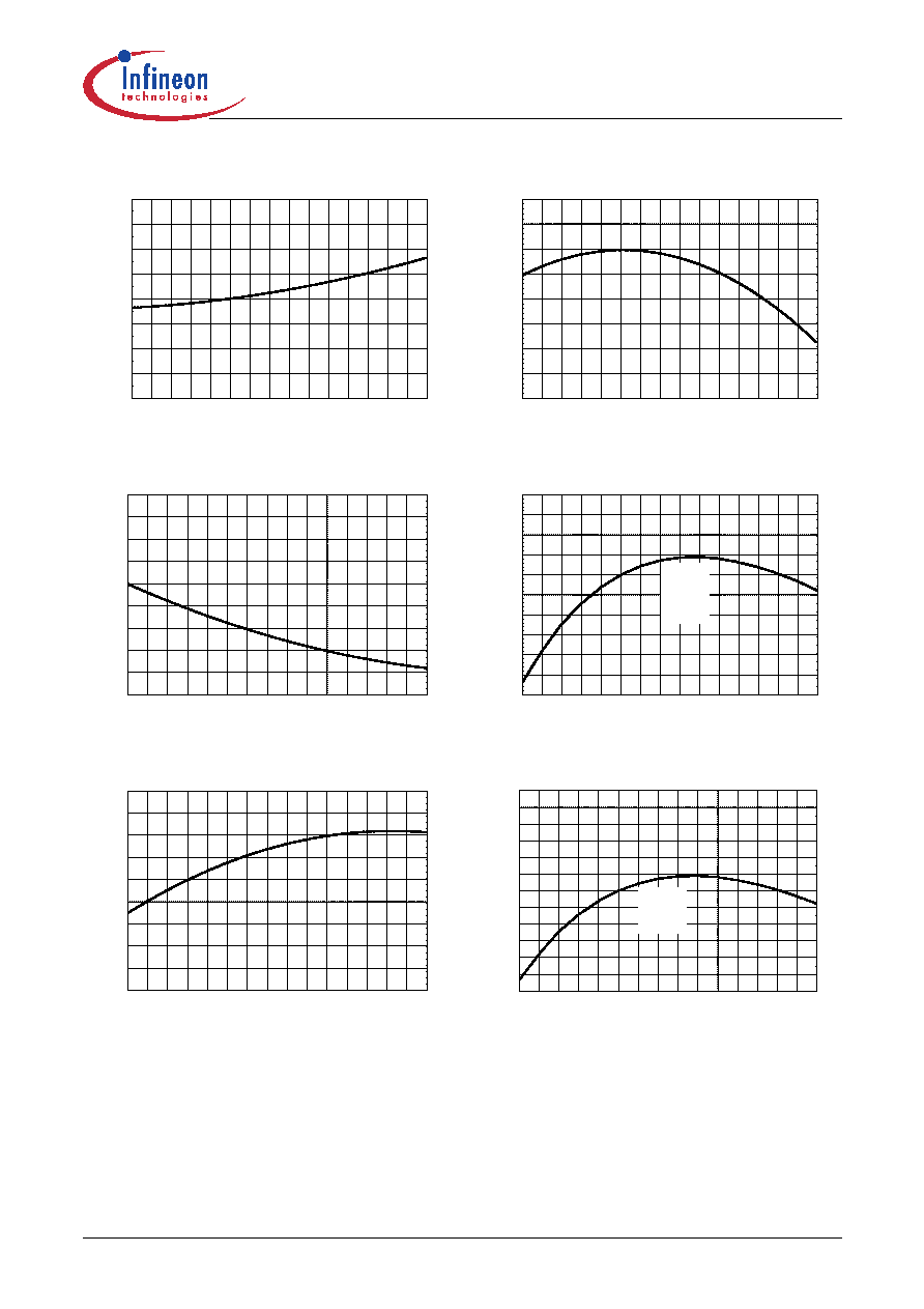
Version 2.0 26 11 Jun 2004
CoolSETTM-F2
Typical Performance Characteristics
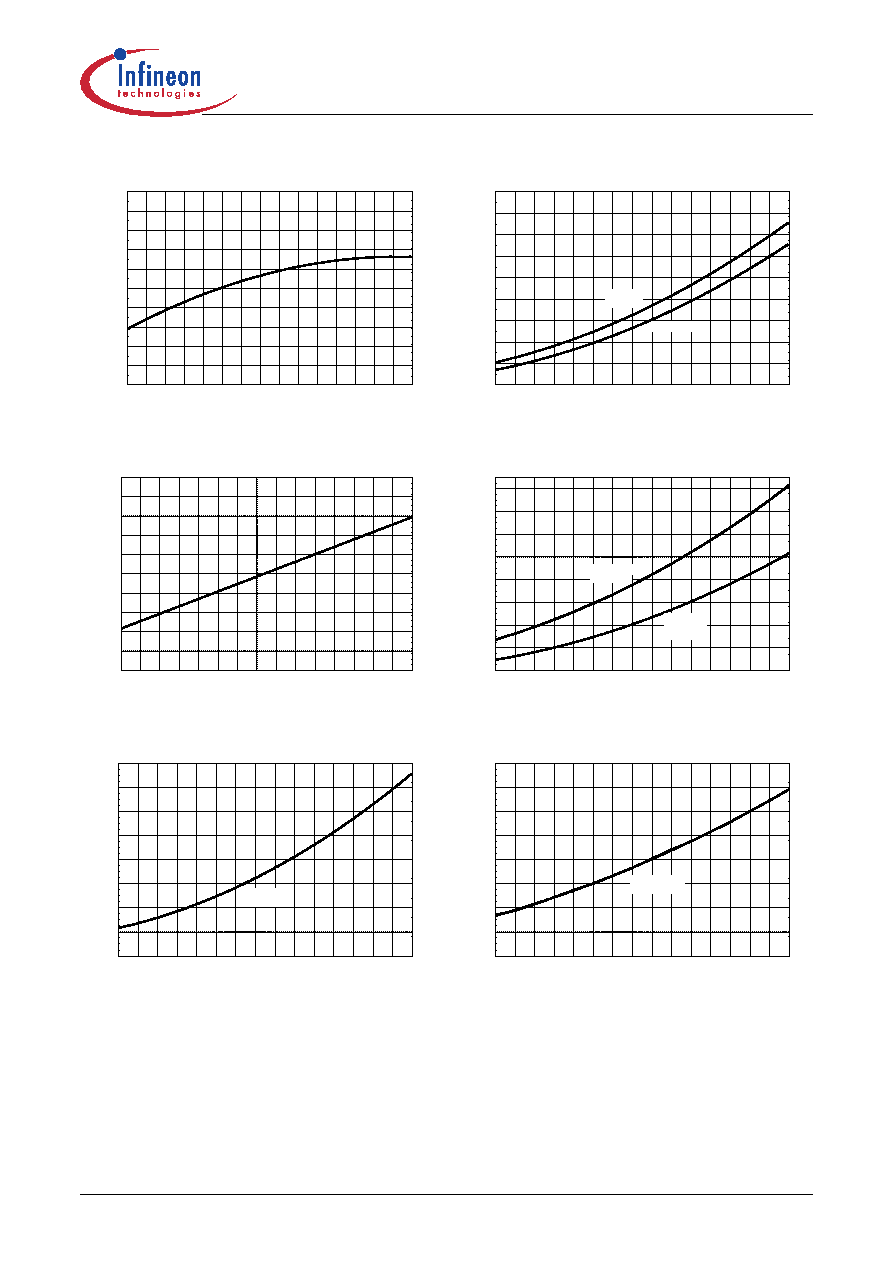
Figure 31
VCC Turn-On Threshold V
CCon
vs. T
j
Figure 32
VCC Turn-Off Threshold V
VCCoff
vs. T
j
Figure 33
VCC Turn-On/Off Hysteresis V
VCCHY
vs. T
j
Figure 34
Trimmed Reference V
REF
vs. T
j
Figure 35
Oscillator Frequency f
OSC1
vs. T
j
Figure 36
Oscillator Frequency f
OSC3
vs. T
j
Junction Temperature [∞C]
VC
C
Turn-On Threshold V
CCon
[V]
P
I
-
004-
190101
13,42
13,44
13,46
13,48
13,50
13,52
13,54
13,56
13,58
-25 -15
-5
5
15
25
35
45
55
65
75
85
95 105 115 125
Junction Temperature [∞C]
VC
C
Turn-Off Threshold V
V
CCof
f
[V]
P
I
-
005-
190101
8,40
8,43
8,46
8,49
8,52
8,55
8,58
8,61
8,64
8,67
-25 -15
-5
5
15
25
35
45
55
65
75
85
95 105 115 125
Junction Temperature [∞C]
VC
C
Turn-On/Off H
ysteresis V
CCHY
[V]
P
I
-
006-
190101
4,83
4,86
4,89
4,92
4,95
4,98
5,01
5,04
5,07
5,10
-25 -15
-5
5
15
25
35
45
55
65
75
85
95 105 115 125
Junction Temperature [∞C]
Trimmed R
e
ference Voltage V
RE
F
[V]
P
I
-
007-
190101
6,470
6,475
6,480
6,485
6,490
6,495
6,500
6,505
6,510
-25 -15
-5
5
15
25
35
45
55
65
75
85
95 105 115 125
Junction Temperature [∞C]
Oscillator Frequency f
OSC
1
[kH
z]
P
I
-
008-
190101
97,0
97,5
98,0
98,5
99,0
99,5
100,0
100,5
101,0
101,5
102,0
-25 -15
-5
5
15
25
35
45
55
65
75
85
95 105 115 125
ICE2A0565
ICE2A165
ICE2A265
ICE2A365
ICE2A180Z
ICE2A280Z
ICE2A765P2
/G/Z
Junction Temperature [∞C]
Oscillator Frequency f
OSC
3
[kHz
]
P
I
-
008a-
190101
64,0
64,5
65,0
65,5
66,0
66,5
67,0
67,5
68,0
68,5
69,0
69,5
70,0
-25 -15
-5
5
15
25
35
45
55
65
75
85
95 105 115 125
ICE2B0565
ICE2B165
ICE2B265
ICE2B365
ICE2B765P2

Version 2.0 27 11 Jun 2004
CoolSETTM-F2
Typical Performance Characteristics
Figure 37
Reduced Osc. Frequency f
OSC2
vs. T
j
Figure 38
Reduced Osc. Frequency f
OSC4
vs. T
j
Figure 39
Frequency Ratio f
OSC1
/ f
OSC2
vs. T
j
Figure 40
Frequency Ratio f
OSC3
/ f
OSC4
vs. T
j
Figure 41
Max. Duty Cycle vs. T
j
Figure 42
PWM-OP Gain A
V
vs. T
j
Junction Temperature [∞C]
Reduced Osc. Frequency f
OSC
2
[kH
z]
P
I
-
009-
190101
20,0
20,2
20,4
20,6
20,8
21,0
21,2
21,4
21,6
21,8
22,0
-25 -15
-5
5
15
25
35
45
55
65
75
85
95 105 115 125
ICE2A0565
ICE2A165
ICE2A265
ICE2A365
ICE2A180Z
ICE2A280Z
ICE2A765P2
/G/Z
Junction Temperature [∞C]
R
e
duced Osc. Frequency f
OS
C
4
[kHz
]
P
I
-
009a-
190101
19,0
19,2
19,4
19,6
19,8
20,0
20,2
20,4
20,6
20,8
21,0
-25 -15
-5
5
15
25
35
45
55
65
75
85
95 105 115 125
ICE2B0565
ICE2B165
ICE2B265
ICE2B365
ICE2B765P2
Junction Temperature [∞C]
Frequency R
a
tio f
OSC
1
/f
OSC
2
P
I
-
010-
190101
4,55
4,57
4,59
4,61
4,63
4,65
4,67
4,69
4,71
4,73
4,75
-25 -15
-5
5
15
25
35
45
55
65
75
85
95 105 115 125
ICE2A0565
ICE2A165
ICE2A265
ICE2A365
ICE2A180Z
ICE2A280Z
ICE2A765P2
/G/Z
Junction Temperature [∞C]
Frequency R
a
tio f
OSC
3
/f
OSC
4
P
I
-
010a-
190101
3,25
3,27
3,29
3,31
3,33
3,35
3,37
3,39
3,41
3,43
3,45
-25 -15
-5
5
15
25
35
45
55
65
75
85
95 105 115 125
ICE2B0565
ICE2B165
ICE2B265
ICE2B365
ICE2B765P2
Junction Temperature [∞C]
Max. D
u
ty C
ycle
P
I
-
011-
190101
0,710
0,712
0,714
0,716
0,718
0,720
0,722
0,724
0,726
0,728
0,730
-25 -15
-5
5
15
25
35
45
55
65
75
85
95 105 115 125
Junction Temperature [∞C]
PWM-OP Gain A
V
P
I
-
012-
190101
3,60
3,61
3,62
3,63
3,64
3,65
3,66
3,67
3,68
3,69
3,70
-25 -15
-5
5
15
25
35
45
55
65
75
85
95 105 115 125

Version 2.0 28 11 Jun 2004
CoolSETTM-F2
Typical Performance Characteristics
Figure 43
Feedback Resistance R
FB
vs. T
j
Figure 44
Soft-Start Resistance R
Soft-Start
vs. T
j
Figure 45
Detection Limit V
FB2
vs. T
j
Figure 46
Detection Limit V
Soft-Start1
vs. T
j
Figure 47
Detection Limit V
Soft-Start2
vs. T
j
Figure 48
Overvoltage Detection Limit V
VCC1
vs. T
j
Junction Temperature [∞C]
Feedback Resistance R
FB
[kOhm]
P
I
-
013-
190101
3,50
3,55
3,60
3,65
3,70
3,75
3,80
3,85
3,90
3,95
4,00
-25 -15
-5
5
15
25
35
45
55
65
75
85
95 105 115 125
Junction Temperature [∞C]
Soft-Start R
esistance R
Soft-Sta
r
t
[kOhm]
P
I
-
014-
190101
40
42
44
46
48
50
52
54
56
58
-25 -15
-5
5
15
25
35
45
55
65
75
85
95 105 115 125
Junction Temperature [∞C]
D
e
tection Limit V
FB2
[V]
P
I
-
015-
190101
4,780
4,785
4,790
4,795
4,800
4,805
4,810
-25 -15
-5
5
15
25
35
45
55
65
75
85
95 105 115 125
Junction Temperature [∞C]
D
e
tection Limit V
Soft-Sta
r
t
1
[V]
P
I
-
016-
190101
5,270
5,275
5,280
5,285
5,290
5,295
5,300
5,305
5,310
5,315
5,320
-25 -15
-5
5
15
25
35
45
55
65
75
85
95 105 115 125
Junction Temperature [∞C]
D
e
tection Limit V
Soft-Sta
r
t
2
[V]
P
I
-
017-
190101
3,95
3,96
3,97
3,98
3,99
4,00
4,01
4,02
4,03
4,04
4,05
-25 -15
-5
5
15
25
35
45
55
65
75
85
95 105 115 125
Junction Temperature [∞C]
Overvoltage Detection Limit V
V
CC1
[V]
P
I
-
018-
190101
16,20
16,25
16,30
16,35
16,40
16,45
16,50
16,55
16,60
16,65
16,70
16,75
16,80
-25 -15
-5
5
15
25
35
45
55
65
75
85
95 105 115 125
Version 2.0 29 11 Jun 2004
CoolSETTM-F2
Typical Performance Characteristics
Figure 49
Peak Current Limitation V
csth
vs. T
j
Figure 50
Leading Edge Blanking V
VCC1
vs. T
j
Figure 51
Drain Source On-Resistance R
DSon
vs. T
j
Figure 52
Drain Source On-Resistance R
DSon
vs. T
j
Figure 53
Drain Source On-Resistance R
DSon
vs. T
j
Figure 54
Drain Source On-Resistance R
DSon
vs. T
j
Junction Temperature [∞C]
Peak Current Limitation V
cst
h
[V]
P
I
-
019-
190101
0,990
0,992
0,994
0,996
0,998
1,000
1,002
1,004
1,006
1,008
1,010
-25 -15
-5
5
15
25
35
45
55
65
75
85
95 105 115 125
Junction Temperature [∞C]
Leading Edge B
l
anking t
LE
B
[ns]
P
I
-
020-
190101
180
190
200
210
220
230
240
250
260
270
280
-25 -15
-5
5
15
25
35
45
55
65
75
85
95 105 115 125
Junction Temperature [∞C]
On-Resistance R
dson
[Ohm]
P
I
-
022-
190101
0,2
0,3
0,4
0,5
0,6
0,7
0,8
0,9
1,0
-25 -15
-5
5
15
25
35
45
55
65
75
85
95 105 115 125
ICE2A365
ICE2B365
Junction Temperature [∞C]
On-Resistance R
dson
[Ohm]
P
I
-
022-
190101
0,4
0,6
0,8
1,0
1,2
1,4
1,6
1,8
2,0
2,2
-25 -15
-5
5
15
25
35
45
55
65
75
85
95 105 115 125
ICE2A280Z
ICE2A265
ICE2B265
Junction Temperature [∞C]
On-Resistance R
dson
[Ohm]
P
I
-
022-
190101
1,5
2,5
3,5
4,5
5,5
6,5
7,5
8,5
9,5
-25 -15
-5
5
15
25
35
45
55
65
75
85
95 105 115 125
ICE2A0565
ICE2B0565
ICE2A165
ICE2B165
ICE2A180Z
/G/Z
Junction Temperature [∞C]
On-Resistance R
dson
[Ohm]
P
I
-
022-
190101
0,2
0,3
0,4
0,5
0,6
0,7
0,8
0,9
1,0
-25 -15
-5
5
15
25
35
45
55
65
75
85
95 105 115 125
ICE2A765P2
ICE2B765P2

Version 2.0 30 11 Jun 2004
CoolSETTM-F2
Typical Performance Characteristics
Figure 55
Breakdown Voltage V
BR(DSS)
vs. T
j
Figure 56
Breakdown Voltage V
BR(DSS)
vs. T
j
Junction Temperature [∞C]
B
r
eakdown Voltage V
(
BR)
DS
S
[V]
P
I
-
025-
190101
560
580
600
620
640
660
680
700
720
-25 -15
-5
5
15
25
35
45
55
65
75
85
95 105 115 125
ICE2A0565
ICE2A165
ICE2A265
ICE2A365
ICE2B0565
ICE2B165
ICE2B265
ICE2B365
ICE2A765P2
ICE2B765P2
/G/Z
Junction Temperature [∞C]
B
r
eakdown Voltage V
(
BR)
DS
S
[V]
P
I
-
025-
190101
780
800
820
840
860
880
900
920
940
-25 -15
-5
5
15
25
35
45
55
65
75
85
95 105 115 125
ICE2A180Z
ICE2A280Z
Version 2.0 31 11 Jun 2004
CoolSETTM-F2
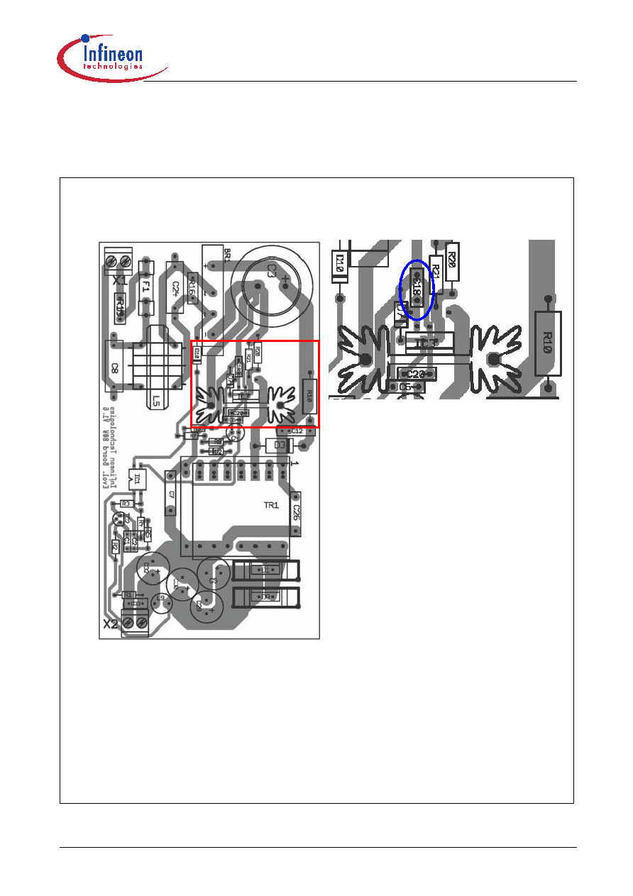
Layout Recommendation for C
18
6
Layout Recommendation for C
18
Note:
Only for ICE2A765I/P2 and ICE2B765I/P2
Figure 57
Layout Recommendation for ICE2A765I/P2 and ICE2B765I/P2
Soft Start Capacitor Layout Recommendation in Detail
Figure 5
7A
Layout of Board EVALSF2_ICE2B765P2
To improve the startup behavior of the IC during
startup or auto restart mode, place the soft start
capacitor C
18
(red section Detail X in Figure 5
7A)
as close as possible to the soft start PIN 6 and
GND PIN 4. More details see Detail X in Figure
5
7B.
Figure 5
7B Detail X, Soft Start Capacitor C
18
Layout
Recommendation
Place Soft Start capacitor C
18
in the same way as
shown in Detail X (blue mark).
Detail X

CoolSETTM-F2
Outline Dimension
Version 2.0 32 11 Jun 2004
7
Outline Dimension
Figure 58
P-DIP-8-6 (Plastic Dual In-line Package)
Figure 59
P-DIP-7-1 (Plastic Dual In-line Package)
Dimensions in mm
P-DIP-8-6
(Plastic Dual In-line
Package)
P-DIP-7-1
(Plastic Dual In-line
Package)
Does not include plastic or metal protrusion of 0.25 max. per side
9.52
Index Marking
±0.25
0.35
2.54
0.46
1
7
±0.1
1.7 MAX.
4
1)
7x
5
3.25 MIN.
4.37 MAX.
0.38 MIN.
±0.25
8.9
±1
0.25
6.35
+0.1
±0.38
7.87
1)
1)
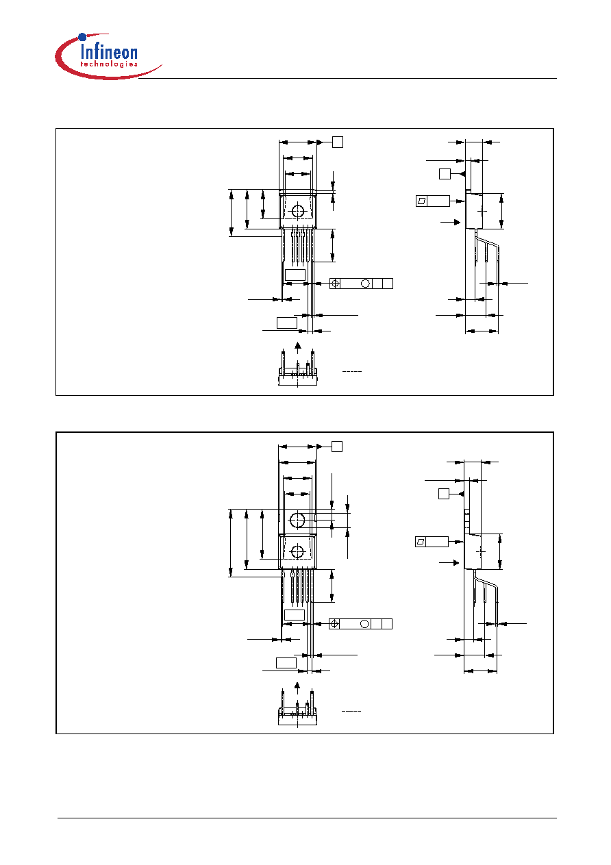
Version 2.0 33 11 Jun 2004
CoolSETTM-F2
Outline Dimension
Figure 60
P-TO220-6-46 (Isodrain Package)
Figure 61
P-TO220-6-47 (Isodrain Package)
Dimensions in mm
B
+0.1
-0.02
1.3
4.4
±0.2
9.2
1)
0.05
±0.3
5.3
8.4
2.4
±0.3
0.5
±0.1
9.9
A
6.6
7.5
±0.3
8.6
4 x 1.27
7.62
0.25
A
M
B
±0.1
6 x 0.6
0...0.15
±0.3
8
±0.3
12.1
10.2
(0.8)
Back side, heatsink contour
1) Shear and punch direction no burrs this surface
All metal surfaces tin plated, except area of cut.
P-TO220-6-46
Isodrain Package
P-TO220-6-47
Isodrain Package
All metal surfaces tin plated, except area of cut.
1) Shear and punch direction no burrs this surface
Back side, heatsink contour
6.6
9.5
±0.2
±0.2
9.9
A
3.7
2.8
-0.15
±0.2
13
±0.3
15.6
±0.3
17.5
7.5
0...0.15
±0.3
8.6
±0.1
6 x 0.6
1.27
4 x
0.25
A
M
B
7.62
1.3
-0.02
4.4
+0.1
B
0.05
1)
±0.1
0.5
2.4
±0.3
5.3
±0.3
8.4
9.2
±0.2
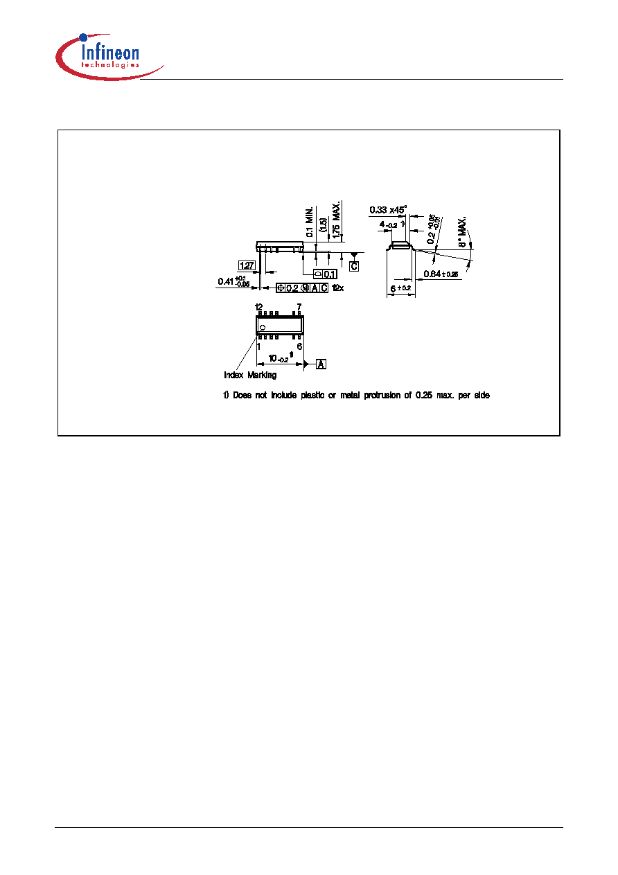
CoolSETTM-F2
Outline Dimension
Version 2.0 34 11 Jun 2004
Figure 62
P-DSO-16/12 (Plastic Dual Small Outline Package)
Dimensions in mm
P-DSO-16/12
(Plastic Dual Small
Outline Package)

Qualit‰t hat f¸r uns eine umfassende
Bedeutung. Wir wollen allen Ihren
Anspr¸chen in der bestmˆglichen
Weise gerecht werden. Es geht uns also
nicht nur um die Produktqualit‰t ≠
unsere Anstrengungen gelten
gleichermaþen der Lieferqualit‰t und
Logistik, dem Service und Support
sowie allen sonstigen Beratungs- und
Betreuungsleistungen.
Dazu gehˆrt eine bestimmte
Geisteshaltung unserer Mitarbeiter.
Total Quality im Denken und Handeln
gegen¸ber Kollegen, Lieferanten und
Ihnen, unserem Kunden. Unsere
Leitlinie ist jede Aufgabe mit ,,Null
Fehlern" zu lˆsen ≠ in offener
Sichtweise auch ¸ber den eigenen
Arbeitsplatz hinaus ≠ und uns st‰ndig
zu verbessern.
Unternehmensweit orientieren wir uns
dabei auch an ,,top" (Time Optimized
Processes), um Ihnen durch grˆþere
Schnelligkeit den entscheidenden
Wettbewerbsvorsprung zu verschaffen.
Geben Sie uns die Chance, hohe
Leistung durch umfassende Qualit‰t zu
beweisen.
Wir werden Sie ¸berzeugen.
Quality takes on an allencompassing
significance at Semiconductor Group.
For us it means living up to each and
every one of your demands in the best
possible way. So we are not only
concerned with product quality. We
direct our efforts equally at quality of
supply and logistics, service and
support, as well as all the other ways in
which we advise and attend to you.
Part of this is the very special attitude of
our staff. Total Quality in thought and
deed, towards co-workers, suppliers
and you, our customer. Our guideline is
"do everything with zero defects", in an
open manner that is demonstrated
beyond your immediate workplace, and
to constantly improve.
Throughout the corporation we also
think in terms of Time Optimized
Processes (top), greater speed on our
part to give you that decisive
competitive edge.
Give us the chance to prove the best of
performance through the best of quality
≠ you will be convinced.
h t t p : / / w w w . i n f i n e o n . c o m
Total Quality Management
Published by Infineon Technologies AG