Äîêóìåíòàöèÿ è îïèñàíèÿ www.docs.chipfind.ru

SKW30N60HS
^
Power Semiconductors
1
Rev. 2 Aug-02
High Speed IGBT in NPT-technology
·
30% lower
E
off
compared to previous generation
·
Short circuit withstand time 10
µ
s
·
Designed for operation above 30 kHz
·
NPT-Technology for 600V applications offers:
- parallel switching capability
- moderate E
off
increase with temperature
- very tight parameter distribution
·
High ruggedness, temperature stable behaviour
·
Complete product spectrum and PSpice Models :
http://www.infineon.com/igbt/
Type
V
CE
I
C
E
off)
T
j
Package
Ordering Code
SKW30N60HS
600V
30
480µJ
150
°
C
TO-247AC
Q67040-S4503
Maximum Ratings
Parameter
Symbol
Value
Unit
Collector-emitter voltage
V
C E
600
V
DC collector current
T
C
= 25
°
C
T
C
= 100
°
C
I
C
41
30
Pulsed collector current,
t
p
limited by
T
jmax
I
C p u l s
112
Turn off safe operating area
V
CE
600V,
T
j
150
°
C
-
112
Diode forward current
T
C
= 25
°
C
T
C
= 100
°
C
I
F
41
28
Diode pulsed current,
t
p
limited by
T
jmax
I
F p u l s
112
A
Gate-emitter voltage static
transient (
t
p
<1µs,
D
<0.05)
V
G E
±
20
±
30
V
Short circuit withstand time
1)
V
GE
= 15V,
V
CC
600V,
T
j
150
°
C
t
S C
10
µ
s
Power dissipation
T
C
= 25
°
C
P
t o t
250
W
Operating junction and storage temperature
T
j
,
T
s t g
-55...+150
Time limited operating junction temperature for
t
< 150h
T
j ( t l )
175
Soldering temperature, 1.6mm (0.063 in.) from case for 10s
-
260
°
C
1)
Allowed number of short circuits: <1000; time between short circuits: >1s.
P-TO-247-3-1
(TO-247AC)
G
C
E

SKW30N60HS
^
Power Semiconductors
2
Rev. 2 Aug-02
Thermal Resistance
Parameter
Symbol
Conditions
Max. Value
Unit
Characteristic
IGBT thermal resistance,
junction case
R
t h J C
0.5
Diode thermal resistance,
junction case
R
t h J C D
1.29
Thermal resistance,
junction ambient
R
t h J A
TO-247AC
40
K/W
Electrical Characteristic,
at
T
j
= 25
°
C, unless otherwise specified
Value
Parameter
Symbol
Conditions
min.
Typ.
max.
Unit
Static Characteristic
Collector-emitter breakdown voltage
V
( B R ) C E S
V
G E
=0V,
I
C
=500
µ
A
600
-
-
Collector-emitter saturation voltage
V
C E ( s a t )
V
G E
= 15V,
I
C
=30A
T
j
=25
°
C
T
j
=150
°
C
2.8
3.5
3.15
4.00
Diode forward voltage
V
F
V
G E
=0V,
I
F
=30A
T
j
=25
°
C
T
j
=150
°
C
-
1.55
1.55
2.05
2.05
Gate-emitter threshold voltage
V
G E ( t h )
I
C
=700
µ
A,
V
C E
=
V
G E
3
4
5
V
Zero gate voltage collector current
I
C E S
V
C E
=600V,
V
G E
=0V
T
j
=25
°
C
T
j
=150
°
C
-
-
-
-
40
3000
µ
A
Gate-emitter leakage current
I
G E S
V
C E
=0V,
V
G E
=20V
-
-
100
nA
Transconductance
g
f s
V
C E
=20V,
I
C
=30A
-
20
S
SKW30N60HS
^
Power Semiconductors
3
Rev. 2 Aug-02
Dynamic Characteristic
Input capacitance
C
i s s
-
1500
Output capacitance
C
o s s
-
203
Reverse transfer capacitance
C
r s s
V
C E
=25V,
V
G E
=0V,
f
=1MHz
-
92
pF
Gate charge
Q
G a t e
V
C C
=480V,
I
C
=30A
V
G E
=15V
-
141
nC
Internal emitter inductance
measured 5mm (0.197 in.) from case
L
E
T O-247AC
-
13
nH
Short circuit collector current
1)
I
C ( S C )
V
G E
=15V,
t
S C
10
µ
s
V
C C
600V,
T
j
150
°
C
-
220
A
Switching Characteristic, Inductive Load,
at
T
j
=25
°
C
Value
Parameter
Symbol
Conditions
min.
typ.
max.
Unit
IGBT Characteristic
Turn-on delay time
t
d ( o n )
-
20
Rise time
t
r
-
21
Turn-off delay time
t
d ( o f f )
-
250
Fall time
t
f
-
25
ns
Turn-on energy
E
o n
-
0.60
Turn-off energy
E
o f f
-
0.55
Total switching energy
E
t s
T
j
=25
°
C,
V
C C
=400V,
I
C
=30A,
V
G E
=0/15V,
R
G
=11
L
2 )
=60nH,
C
2 )
=40pF
Energy losses include
"tail" and diode
reverse recovery.
-
1.15
mJ
Anti-Parallel Diode Characteristic
Diode reverse recovery time
t
r r
t
S
t
F
-
-
-
125
20
105
ns
Diode reverse recovery charge
Q
r r
-
0.82
µC
Diode peak reverse recovery current
I
r r m
-
17
A
Diode peak rate of fall of reverse
recovery current during
t
b
di
r r
/dt
T
j
=25
°
C,
V
R
=400V,
I
F
=30A,
di
F
/dt
=1100A/
µ
s
-
580
A/
µ
s
1)
Allowed number of short circuits: <1000; time between short circuits: >1s.
2)
Leakage inductance
L
and Stray capacity
C
due to test circuit in Figure E.
SKW30N60HS
^
Power Semiconductors
4
Rev. 2 Aug-02
Switching Characteristic, Inductive Load,
at
T
j
=150
°
C
Value
Parameter
Symbol
Conditions
min.
typ.
max.
Unit
IGBT Characteristic
Turn-on delay time
t
d ( o n )
-
16
Rise time
t
r
-
13
Turn-off delay time
t
d ( o f f )
-
122
Fall time
t
f
-
29
ns
Turn-on energy
E
o n
-
0.78
Turn-off energy
E
o f f
-
0.48
Total switching energy
E
t s
T
j
=150
°
C
V
C C
=400V,
I
C
=30A,
V
G E
=0/15V,
R
G
= 1.8
L
1 )
=60nH,
C
1 )
=40pF
Energy losses include
"tail" and diode
reverse recovery.
-
1.26
mJ
Turn-on delay time
t
d ( o n )
-
20
Rise time
t
r
-
19
Turn-off delay time
t
d ( o f f )
-
274
Fall time
t
f
-
27
ns
Turn-on energy
E
o n
-
0.91
Turn-off energy
E
o f f
-
0.70
Total switching energy
E
t s
T
j
=150
°
C
V
C C
=400V,
I
C
=30A,
V
G E
=0/15V,
R
G
= 11
L
1 )
=60nH,
C
1 )
=40pF
Energy losses include
"tail" and diode
reverse recovery.
-
1.61
mJ
Anti-Parallel Diode Characteristic
Diode reverse recovery time
t
r r
t
S
t
F
-
-
-
190
30
160
ns
Diode reverse recovery charge
Q
r r
-
2.0
µC
Diode peak reverse recovery current
I
r r m
-
24
A
Diode peak rate of fall of reverse
recovery current during
t
b
di
r r
/dt
T
j
=150
°
C
V
R
=400V,
I
F
=30A,
di
F
/dt
=1250A/
µ
s
-
480
A/
µ
s
1)
Leakage inductance
L
and Stray capacity
C
due to test circuit in Figure E.
SKW30N60HS
^
Power Semiconductors
5
Rev. 2 Aug-02
I
C
,
COLLE
CT
OR CURRE
N
T
10Hz
100Hz
1kHz
10kHz
100kHz
0A
20A
40A
60A
80A
100A
T
C
=80°C
T
C
=110°C
I
C
,
COLLE
CT
OR CURRE
N
T
1V
10V
100V
1000V
0,1A
1A
10A
100A
t
P
=4µs
15µs
200µs
1ms
50µs
DC
f
,
SWITCHING FREQUENCY
V
CE
,
COLLECTOR
-
EMITTER VOLTAGE
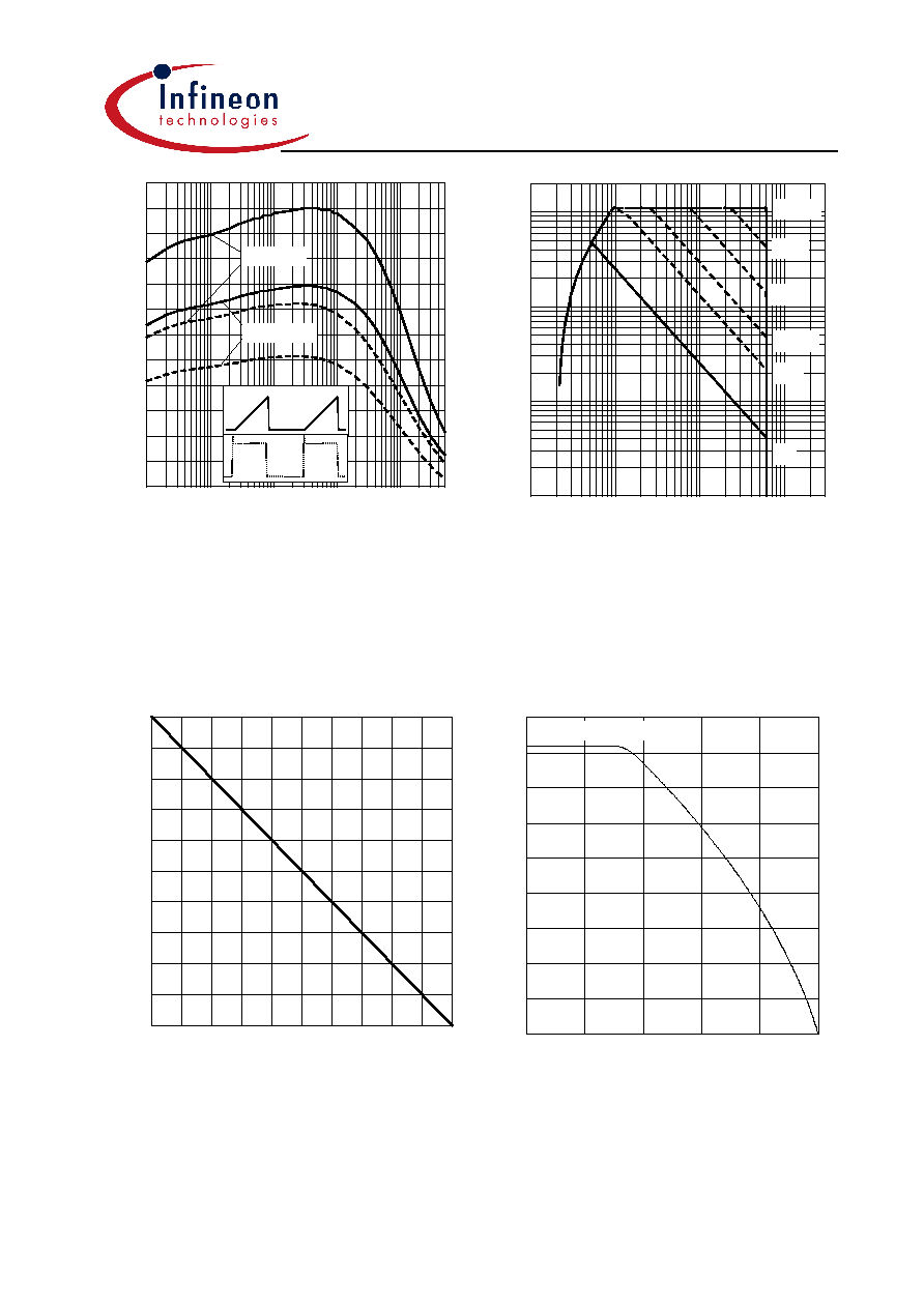
Figure 1. Collector current as a function of
switching frequency
(
T
j
150
°
C,
D =
0.5,
V
CE
= 400V,
V
GE
= 0/+15V,
R
G
= 11
)
Figure 2. Safe operating area
(
D =
0,
T
C
= 25
°
C,
T
j
150
°
C;
V
GE
=15V)
P
tot
,
P
O
WE
R DIS
S
I
P
A
T
I
O
N
2 5 °C
5 0°C
75 °C
10 0 °C
1 2 5°C
0 W
5 0 W
10 0 W
15 0 W
20 0 W
I
C
,
COLLE
CT
OR CURRE
NT
25°C
75°C
125°C
0A
10A
20A
30A
40A
T
C
,
CASE TEMPERATURE
T
C
,
CASE TEMPERATURE
Figure 3. Power dissipation as a function of
case temperature
(
T
j
150
°
C)
Figure 4. Collector current as a function of
case temperature
(
V
GE
15V,
T
j
150
°
C)
Limited by Bond wire
I
c
I
c