Äîêóìåíòàöèÿ è îïèñàíèÿ www.docs.chipfind.ru
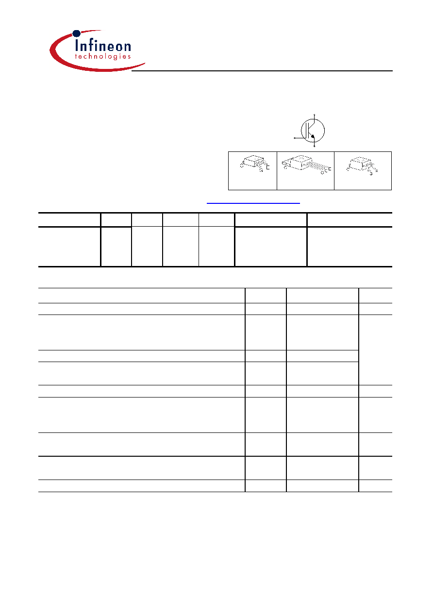
SGP02N60,
SGB02N60
SGD02N60
1
Jul-02
Fast IGBT in NPT-technology
·
75% lower E
off
compared to previous generation
combined with low conduction losses
·
Short circuit withstand time 10
µ
s
·
Designed for:
- Motor controls
- Inverter
·
NPT-Technology for 600V applications offers:
- very tight parameter distribution
- high ruggedness, temperature stable behaviour
- parallel switching capability
·
Complete product spectrum and PSpice Models :
http://www.infineon.com/igbt/
Type
V
CE
I
C
V
CE(sat)
T
j
Package
Ordering Code
SGP02N60
600V
2A
2.2V
150
°
C
TO-220AB
Q67040-S4504
SGB02N60
SGD02N60
TO-263AB
TO-252AA(DPAK)
Q67040-S4505
Q67041-A4707
Maximum Ratings
Parameter
Symbol
Value
Unit
Collector-emitter voltage
V
C E
600
V
DC collector current
T
C
= 25
°
C
T
C
= 100
°
C
I
C
6.0
2.9
Pulsed collector current, t
p
limited by T
jmax
I
C p u l s
12
Turn off safe operating area
V
CE
600V, T
j
150
°
C
-
12
A
Gate-emitter voltage
V
G E
±
20
V
Avalanche energy, single pulse
I
C
= 2 A, V
CC
= 50 V, R
GE
= 25
,
start at T
j
= 25
°
C
E
A S
13
mJ
Short circuit withstand time
1)
V
GE
= 15V, V
CC
600V, T
j
150
°
C
t
S C
10
µ
s
Power dissipation
T
C
= 25
°
C
P
t o t
30
W
Operating junction and storage temperature
T
j
, T
s t g
-55...+150
°
C
1)
Allowed number of short circuits: <1000; time between short circuits: >1s.
G
C
E
P-TO-220-3-1
(TO-220AB)
P-TO-252-3-1 (D-PAK)
(TO-252AA)
P-TO-263-3-2 (D²-PAK)
(TO-263AB)
SGP02N60,
SGB02N60
SGD02N60
2
Jul-02
Thermal Resistance
Parameter
Symbol
Conditions
Max. Value
Unit
Characteristic
IGBT thermal resistance,
junction case
R
t h J C
4.2
Thermal resistance,
junction ambient
R
t h J A
TO-220AB
62
SMD version, device on PCB
1)
R
t h J A
TO-252AA
TO-263AB
50
40
K/W
Electrical Characteristic, at T
j
= 25
°
C, unless otherwise specified
Value
Parameter
Symbol
Conditions
min.
Typ.
max.
Unit
Static Characteristic
Collector-emitter breakdown voltage
V
( B R ) C E S
V
G E
=0V, I
C
=500
µ
A
600
-
-
Collector-emitter saturation voltage
V
C E ( s a t )
V
G E
= 15V, I
C
=2A
T
j
=25
°
C
T
j
=150
°
C
1.7
-
1.9
2.2
2.4
2.7
Gate-emitter threshold voltage
V
G E ( t h )
I
C
=150
µ
A,V
C E
=V
G E
3
4
5
V
Zero gate voltage collector current
I
C E S
V
C E
=600V,V
G E
=0V
T
j
=25
°
C
T
j
=150
°
C
-
-
-
-
20
250
µ
A
Gate-emitter leakage current
I
G E S
V
C E
=0V,V
G E
=20V
-
-
100
nA
Transconductance
g
f s
V
C E
=20V, I
C
=2A
-
1.6
-
S
Dynamic Characteristic
Input capacitance
C
i s s
-
142
170
Output capacitance
C
o s s
-
18
22
Reverse transfer capacitance
C
r s s
V
C E
=25V,
V
G E
=0V,
f=1MHz
-
10
12
pF
Gate charge
Q
G a t e
V
C C
=480V, I
C
=2A
V
G E
=15V
-
14
18
nC
Internal emitter inductance
measured 5mm (0.197 in.) from case
L
E
T O-220AB
-
7
-
nH
Short circuit collector current
2)
I
C ( S C )
V
G E
=15V,t
S C
10
µ
s
V
C C
600V,
T
j
150
°
C
-
20
-
A
1)
Device on 50mm*50mm*1.5mm epoxy PCB FR4 with 6cm
2
(one layer, 70
µ
m thick) copper area for
collector connection. PCB is vertical without blown air.
2)
Allowed number of short circuits: <1000; time between short circuits: >1s.
SGP02N60,
SGB02N60
SGD02N60
3
Jul-02
Switching Characteristic, Inductive Load, at T
j
=25
°
C
Value
Parameter
Symbol
Conditions
min.
typ.
max.
Unit
IGBT Characteristic
Turn-on delay time
t
d ( o n )
-
20
24
Rise time
t
r
-
13
16
Turn-off delay time
t
d ( o f f )
-
259
311
Fall time
t
f
-
52
62
ns
Turn-on energy
E
o n
-
0.036
0.041
Turn-off energy
E
o f f
-
0.028
0.036
Total switching energy
E
t s
T
j
=25
°
C,
V
C C
=400V,I
C
=2A,
V
G E
=0/15V,
R
G
=118
,
L
1 )
=180nH,
C
1 )
=180pF
Energy losses include
"tail" and diode
reverse recovery.
-
0.064
0.078
mJ
Switching Characteristic, Inductive Load, at T
j
=150
°
C
Value
Parameter
Symbol
Conditions
min.
typ.
max.
Unit
IGBT Characteristic
Turn-on delay time
t
d ( o n )
-
20
24
Rise time
t
r
-
14
17
Turn-off delay time
t
d ( o f f )
-
287
344
Fall time
t
f
-
67
80
ns
Turn-on energy
E
o n
-
0.054
0.062
Turn-off energy
E
o f f
-
0.043
0.056
Total switching energy
E
t s
T
j
=150
°
C,
V
C C
=400V, I
C
=2A,
V
G E
=0/15V,
R
G
=118
,
L
1 )
=180nH,
C
1 )
=180pF
Energy losses include
"tail" and diode
reverse recovery.
-
0.097
0.118
mJ
1)
Leakage inductance L
and Stray capacity C
due to dynamic test circuit in Figure E.
SGP02N60,
SGB02N60
SGD02N60
4
Jul-02
I
C
,
COLLE
CT
OR CURRE
NT
10Hz
100Hz
1kHz
10kHz
100kHz
0A
2A
4A
6A
8A
10A
12A
14A
16A
T
C
=110°C
T
C
=80°C
I
C
,
COLLE
CT
OR CURRE
NT
1V
10V
100V
1000V
0.01A
0.1A
1A
10A
DC
1ms
200
µ
s
50
µ
s
15
µ
s
t
p
=2
µ
s
f,
SWITCHING FREQUENCY
V
CE
,
COLLECTOR
-
EMITTER VOLTAGE
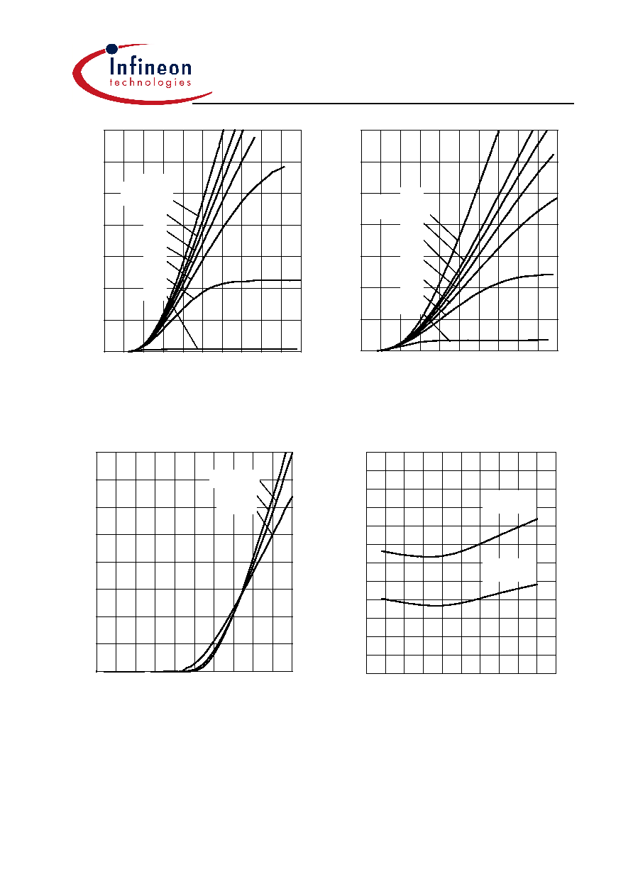
Figure 1. Collector current as a function of
switching frequency
(T
j
150
°
C, D = 0.5, V
CE
= 400V,
V
GE
= 0/+15V, R
G
= 118
)
Figure 2. Safe operating area
(D = 0, T
C
= 25
°
C, T
j
150
°
C)
P
tot
,
PO
W
E
R
D
I
SS
IP
AT
IO
N
25°C
50°C
75°C
100°C 125°C
0W
5W
10W
15W
20W
25W
30W
35W
I
C
,
COLLE
CT
OR CURRE
N
T
25°C
50°C
75°C
100°C
125°C
0A
1A
2A
3A
4A
5A
6A
7A
T
C
,
CASE TEMPERATURE
T
C
,
CASE TEMPERATURE
Figure 3. Power dissipation (IGBT) as a
function of case temperature
(T
j
150
°
C)
Figure 4. Collector current as a function of
case temperature
(V
GE
15V, T
j
150
°
C)
I
c
I
c
SGP02N60,
SGB02N60
SGD02N60
5
Jul-02
I
C
,
COLLE
CT
OR CURRE
NT
0V
1V
2V
3V
4V
5V
0A
1A
2A
3A
4A
5A
6A
7A
15V
13V
11V
9V
7V
5V
V
G E
=20V
I
C
,
COLLE
CT
OR CURRE
NT
0V
1V
2V
3V
4V
5V
0A
1A
2A
3A
4A
5A
6A
7A
15V
13V
11V
9V
7V
5V
V
G E
=20V
V
CE
,
COLLECTOR
-
EMITTER VOLTAGE
V
CE
,
COLLECTOR
-
EMITTER VOLTAGE
Figure 5. Typical output characteristics
(T
j
= 25
°
C)
Figure 6. Typical output characteristics
(T
j
= 150
°
C)
I
C
,
COLLE
CT
OR CURRE
N
T
0V
2V
4V
6V
8V
10V
0A
1A
2A
3A
4A
5A
6A
7A
8A
-55°C
+150°C
T
j
=+25°C
V
CE(sat)
,
COLLE
CTOR
-
EM
ITT
E
R
SATU
R
ATI
O
N
VO
L
T
AG
E
-50°C
0°C
50°C
100°C 150°C
1.0V
1.5V
2.0V
2.5V
3.0V
3.5V
4.0V
V
GE
,
GATE
-
EMITTER VOLTAGE
T
j
,
JUNCTION TEMPERATURE
Figure 7. Typical transfer characteristics
(V
CE
= 10V)
Figure 8. Typical collector-emitter
saturation voltage as a function of junction
temperature
(V
GE
= 15V)
I
C
= 2A
I
C
= 4A