
PWM-FF IC
I C E 3 D S 0 1 L
I C E 3 D S 0 1 L G
O f f - L i n e S M P S C u r r e n t M o d e
C o n t r o l l e r w i t h i n t e g r a t e d 5 0 0 V
S t a r t u p C e l l
N e v e r s t o p t h i n k i n g .
P o w e r M a n a g e m e n t & S u p p l y
D a t a s h e e t , V 2 . 0 , 1 5 M a y 2 0 0 3

Edition 2003-05-15
Published by Infineon Technologies AG,
St.-Martin-Strasse 53,
D-81541 M¸nchen
©
Infineon Technologies AG 1999.
All Rights Reserved.
Attention please!
The information herein is given to describe certain components and shall not be considered as warranted char-
acteristics.
Terms of delivery and rights to technical change reserved.
We hereby disclaim any and all warranties, including but not limited to warranties of non-infringement, regarding
circuits, descriptions and charts stated herein.
Infineon Technologies is an approved CECC manufacturer.
Information
For further information on technology, delivery terms and conditions and prices please contact your nearest Infin-
eon Technologies Office in Germany or our Infineon Technologies Representatives worldwide (see address list).
Warnings
Due to technical requirements components may contain dangerous substances. For information on the types in
question please contact your nearest Infineon Technologies Office.
Infineon Technologies Components may only be used in life-support devices or systems with the express written
approval of Infineon Technologies, if a failure of such components can reasonably be expected to cause the failure
of that life-support device or system, or to affect the safety or effectiveness of that device or system. Life support
devices or systems are intended to be implanted in the human body, or to support and/or maintain and sustain
and/or protect human life. If they fail, it is reasonable to assume that the health of the user or other persons may
be endangered.
For questions on technology, delivery and prices please contact the Infineon Technologies Offices in Germany or
the Infineon Technologies Companies and Representatives worldwide: see our webpage at http://
www.infineon.com
CoolMOSTM, CoolSETTM are trademarks of Infineon Technologies AG.
ICE3DSO1L(G)
Revision History: 2003-05-15 Datasheet
Previous Version:
Page
Subjects (major changes since last revision)

Type
Ordering Code
F
OSC
Package
ICE3DS01L
ES Samples available
110kHz
P-DIP-8-6
ICE3DS01LG
Q67040-S4549-A102
110kHz
P-DSO-8-8
Version 2.0 3 15 May 2003
F3
ICE3DS01L
ICE3DS01LG
C
SoftS
C
VCC
C
Bulk
Converter
DC Output
+
ICE3DS01/G
Snubber
Power
Management
PWM Controller
Current Mode
85 ... 270 VAC
Typical Application
R
Sense
Gate
CS
Startup Cell
HV
Precise Low
Tolerance Peak
Current Limitation
SoftS
FB
GND
VCC
Active Burst Mode
Latched Off Mode
Auto Restart Mode
Control Unit
-
Off-Line SMPS Current Mode Controller
with integrated 500V Startup Cell
test
P-DIP-8-6
P-DSO-8-8
Product Highlights
∑ Active Burst Mode to reach the lowest
Standby Power Requirements < 100mW
∑ Latched Off Mode to increase Robustness
and Safety of the System
∑ Adjustable Blanking Window for High Load
Jumps to increase Reliability
Features
∑
Active Burst Mode for lowest Standby Power
@ light load controlled by Feedback Signal
∑
Fast Load Jump Response in Active Burst Mode
∑
500V Startup Cell switched off after Start Up
∑
110kHz internally fixed Switching Frequency
∑
Latched Off Mode for Overtemperature Detection
∑
Latched Off Mode for Overvoltage Detection
∑
Latched Off Mode for Short Winding Detection
∑
Auto Restart Mode for Overload and Open Loop
∑
Auto Restart Mode for VCC Undervoltage
∑
User defined Soft Start
∑
Minimum of external Components required
∑
Max Duty Cycle 72%
∑
Overall Tolerance of Current Limiting
<
±5%
∑
Internal Leading Edge Blanking
∑
Soft Switching for Low EMI
Description
The F3 Controller provides Active Burst Mode to reach the
lowest Standby Power Requirements <100mW at no load.
As during Active Burst Mode the controller is always active
there is an immediate response on load jumps possible
without any black out in the SMPS. In Active Burst Mode
the ripple of the output voltage can be reduced <1%.
Furthermore Latched Off Mode is entered in case of
Overtemperature, Overvoltage or Short Winding. If
Latched Off Mode is entered only the disconnection from
the main line can reset the Controller. Auto Restart Mode
is entered in case of failure modes like open loop or
overload. By means of the internal precise peak current
limitation the dimension of the transformer and the
secondary diode can be lower which leads to more cost
efficiency. An adjustable blanking window prevents the IC
from entering Auto Restart Mode or Active Burst Mode in
case of high Load Jumps.

F3
ICE3DS01L/LG
Table of Contents
Page
Version 2.0 4 15 May 2003
1
Pin Configuration and Functionality . . . . . . . . . . . . . . . . . . . . . . . . . . . . .5
1.1
Pin Configuration with P-DIP-8-6 . . . . . . . . . . . . . . . . . . . . . . . . . . . . . . . . . .5
1.2
Pin Configuration with P-DSO-8-8 . . . . . . . . . . . . . . . . . . . . . . . . . . . . . . . . .5
1.3
Pin Functionality . . . . . . . . . . . . . . . . . . . . . . . . . . . . . . . . . . . . . . . . . . . . . .6
2
Representative Blockdiagram . . . . . . . . . . . . . . . . . . . . . . . . . . . . . . . . . .7
3
Functional Description . . . . . . . . . . . . . . . . . . . . . . . . . . . . . . . . . . . . . . . .8
3.1
Introduction . . . . . . . . . . . . . . . . . . . . . . . . . . . . . . . . . . . . . . . . . . . . . . . . . .8
3.2
Power Management . . . . . . . . . . . . . . . . . . . . . . . . . . . . . . . . . . . . . . . . . . . .8
3.3
Startup Phase . . . . . . . . . . . . . . . . . . . . . . . . . . . . . . . . . . . . . . . . . . . . . . . .9
3.4
PWM Section . . . . . . . . . . . . . . . . . . . . . . . . . . . . . . . . . . . . . . . . . . . . . . . .10
3.4.1
Oscillator . . . . . . . . . . . . . . . . . . . . . . . . . . . . . . . . . . . . . . . . . . . . . . . . .10
3.4.2
PWM-Latch FF1 . . . . . . . . . . . . . . . . . . . . . . . . . . . . . . . . . . . . . . . . . . . .10
3.4.3
Gate Driver . . . . . . . . . . . . . . . . . . . . . . . . . . . . . . . . . . . . . . . . . . . . . . .10
3.5
Current Limiting . . . . . . . . . . . . . . . . . . . . . . . . . . . . . . . . . . . . . . . . . . . . . .11
3.5.1
Leading Edge Blanking . . . . . . . . . . . . . . . . . . . . . . . . . . . . . . . . . . . . . .11
3.5.2
Propagation Delay Compensation . . . . . . . . . . . . . . . . . . . . . . . . . . . . . .11
3.6
Control Unit . . . . . . . . . . . . . . . . . . . . . . . . . . . . . . . . . . . . . . . . . . . . . . . . .12
3.6.1
Adjustable Blanking Window . . . . . . . . . . . . . . . . . . . . . . . . . . . . . . . . . .12
3.6.2
Active Burst Mode . . . . . . . . . . . . . . . . . . . . . . . . . . . . . . . . . . . . . . . . . .13
3.6.2.1
Entering Active Burst Mode . . . . . . . . . . . . . . . . . . . . . . . . . . . . . . . . .13
3.6.2.2
Working in Active Burst Mode . . . . . . . . . . . . . . . . . . . . . . . . . . . . . . .13
3.6.2.3
Leaving Active Burst Mode . . . . . . . . . . . . . . . . . . . . . . . . . . . . . . . . .13
3.6.3
Protection Modes . . . . . . . . . . . . . . . . . . . . . . . . . . . . . . . . . . . . . . . . . . .14
3.6.3.1
Latched Off Mode . . . . . . . . . . . . . . . . . . . . . . . . . . . . . . . . . . . . . . . .14
3.6.3.2
Auto Restart Mode . . . . . . . . . . . . . . . . . . . . . . . . . . . . . . . . . . . . . . . .15
4
Electrical Characteristics . . . . . . . . . . . . . . . . . . . . . . . . . . . . . . . . . . . . .16
4.1
Absolute Maximum Ratings . . . . . . . . . . . . . . . . . . . . . . . . . . . . . . . . . . . . .16
4.2
Operating Range . . . . . . . . . . . . . . . . . . . . . . . . . . . . . . . . . . . . . . . . . . . . .16
4.3
Characteristics . . . . . . . . . . . . . . . . . . . . . . . . . . . . . . . . . . . . . . . . . . . . . . .17
4.3.1
Supply Section . . . . . . . . . . . . . . . . . . . . . . . . . . . . . . . . . . . . . . . . . . . . .17
4.3.2
Internal Voltage Reference . . . . . . . . . . . . . . . . . . . . . . . . . . . . . . . . . . .17
4.3.3
PWM Section . . . . . . . . . . . . . . . . . . . . . . . . . . . . . . . . . . . . . . . . . . . . . .18
4.3.4
Control Unit . . . . . . . . . . . . . . . . . . . . . . . . . . . . . . . . . . . . . . . . . . . . . . .18
4.3.5
Current Limiting . . . . . . . . . . . . . . . . . . . . . . . . . . . . . . . . . . . . . . . . . . . .19
4.3.6
Driver Section . . . . . . . . . . . . . . . . . . . . . . . . . . . . . . . . . . . . . . . . . . . . .19
5
Typical Performance Characteristics . . . . . . . . . . . . . . . . . . . . . . . . . . .20
6
Outline Dimension . . . . . . . . . . . . . . . . . . . . . . . . . . . . . . . . . . . . . . . . . . .26

Version 2.0 5 15 May 2003
F3
ICE3DS01L/LG
Pin Configuration and Functionality
1
Pin Configuration and Functionality
1.1
Pin Configuration with P-DIP-8-6
Figure 1
Pin Configuration P-DIP-8-6(top view)
Note:
Pin 4 and 5 are shorted within the DIP
package.
1.2
Pin Configuration with P-DSO-8-8
Figure 2
Pin Configuration P-DSO-8-8(top view)
Pin
Symbol
Function
1
SoftS
Soft-Start
2
FB
Feedback
3
CS
Current Sense
4
HV
High Voltage Input
5
HV
High Voltage Input
6
Gate
Driver Stage Output
7
VCC
Controller Supply Voltage
8
GND
Controller Ground
Package P-DIP-8-6
1
6
7
8
4
3
2
5
GND
SoftS
FB
CS
VCC
Gate
HV
HV
Pin
Symbol
Function
1
SoftS
Soft-Start
2
FB
Feedback
3
CS
Current Sense
4
Gate
Driver Stage Output
5
HV
High Voltage Input
6
N.C.
Not connected
7
VCC
Controller Supply Voltage
8
GND
Controller Ground
Package P-DSO-8-8
1
6
7
8
4
3
2
5
GND
SoftS
FB
CS
VCC
N.C.
Gate
HV

Version 2.0 6 15 May 2003
F3
ICE3DS01L/LG
Pin Configuration and Functionality
1.3
Pin Functionality
SoftS (Soft Start & Auto Restart Control)
The SoftS pin combines the function of Soft Start in
case of Start Up and Auto Restart Mode and the
controlling of the Auto Restart Mode in case of error
detection. Furthermore the blanking window for high
load jumps is adjusted by means of the external
capacitor connected to SoftS.
FB (Feedback)
The information about the regulation is provided by the
FB Pin to the internal Protection Unit and to the internal
PWM-Comparator to control the duty cycle. The FB-
Signal controls in case of light load the Active Burst
Mode of the controller.
CS (Current Sense)
The Current Sense pin senses the voltage developed
on the series resistor inserted in the source of the
external PowerMOS. If CS reaches the internal
threshold of the Current Limit Comparator, the Driver
output is immediately switched off. Furthermore the
current information is provided for the PWM-
Comparator to realize the Current Mode.
Gate
The Gate pin is the output of the internal driver stage
connected to the Gate of an external PowerMOS.
HV (High Voltage)
The HV pin is connected to the rectified DC input
voltage. It is the input for the integrated 500V Startup
Cell.
VCC (Power supply)
The VCC pin is the positive supply of the IC. The
operating range is between 8.5V and 21V.
GND (Ground)
The GND pin is the ground of the controller.
F3
ICE3DS01L/LG
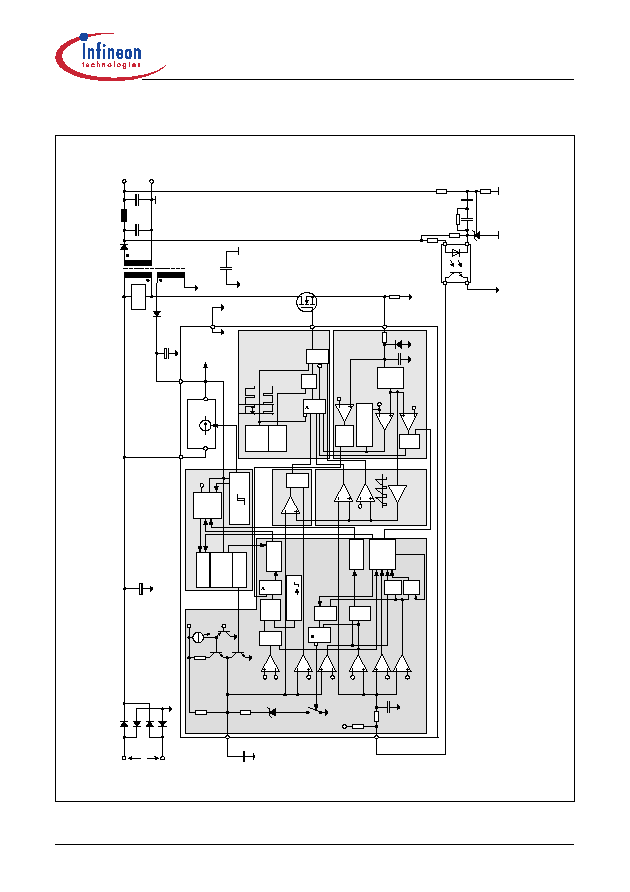
Representative Blockdiagram
Version 2.0 7 15 May 2003
2
Representative Blockdiagram
Figure 3
Representative Blockdiagram
In
te
rn
a
l
B
i
a
s
Vo
l
t
a
g
e
Re
f
e
r
e
n
c
e
O
s
c
ill
a
t
o
r
D
u
t
y C
ycl
e
ma
x
C1
1
x3
.
7
S
o
ft
-S
ta
rt
C
o
m
p
ar
a
t
or
C
u
r
r
e
n
t L
i
m
i
tin
g
PW
M
O
P
C
ur
r
e
nt
M
o
de
Sof
t
St
a
r
t
C2
C1
21
V
4.
0
V
R
FB
Pow
e
r
M
a
na
ge
m
e
n
t
C
So
f
t
S
C
VCC
8
5
...
2
7
0
V
A
C
C
Bu
l
k
+
Co
n
v
e
r
t
e
r
D
C
O
u
tp
u
t
V
OUT
I
C
E
3
D
S
01/
G
S
nu
bbe
r
Sp
i
k
e
B
l
ank
ing
8.0us
PW
M
C
o
m
p
ar
a
t
or
C3
5.
4V
C4
4.
8
V
R
S
o
ftS
Ga
t
e
Dr
i
v
e
r
0.
72
Cl
o
c
k
R
S
ense
Ga
t
e
0.
85V
C9
0.
3V
10
k
D1
T2
C6
1.
3
2V
C5
4.
0
V
C1
0
1.
6
6V
R
S
Q
VC
C
Ac
t
i
v
e
Bu
r
s
t
Mo
d
e
Au
t
o
Re
s
t
a
r
t
Mo
d
e
&
G7
&
G5
&
G9
1
G8
&
G1
1
G3
Th
er
m
a
l
S
h
u
t
do
w
n
T
j
>140∞
C
3.
2
5k
4.
4
V
S1
6.
5
V
&
G4
1
T1
P
o
w
e
r-D
o
w
n
Re
s
e
t
Lat
c
hed
O
f
f
Mo
d
e
R
e
s
e
t
V
VCC
< 6
V
La
t
c
he
d
O
f
f
Mo
d
e
CS
S
o
ftS
GN
D
VC
C
C7
C8
FB
P
W
M
S
ect
i
o
n
C
o
n
t
r
o
l U
n
it
FF1
T3
C1
2
&
0.
2
57V
Lea
di
ng
Ed
g
e
Bl
a
n
k
i
n
g
2
20n
s
5k
10
pF
6.
5
V
G1
0
Sp
i
k
e
B
l
ank
i
n
g
190
ns
1V
5k
1p
F
P
r
op
aga
t
i
on
-
D
el
ay
Co
m
p
e
n
s
a
t
i
o
n
6.
5
V
U
n
de
r
v
ol
t
a
ge Loc
k
o
ut
15V
8.
5V
V
cs
t
h
HV
VC
C
St
a
r
t
u
p C
e
l
l
&
G6
G1
1
G2
&
-

Version 2.0 8 15 May 2003
F3
ICE3DS01L/LG
Functional Description
3
Functional Description
All values which are used in the functional description
are typical values. For calculating the worst cases the
min/max values which can be found in section 4
Electrical Characteristics have to be considered.
3.1
Introduction
The F3 is the further development of the F2 to meet the
requirements for the lowest Standby Power at
minimum load and no load conditions. A new fully
integrated Standby Power concept is implemented into
the IC in order to keep the application design easy.
Compared to F2 no further external parts are needed to
achieve the lowest Standby Power. An intelligent
Active Burst Mode is used for this Standby Mode. After
entering this mode there is still a full control of the
power conversion by the secondary side via the same
optocoupler that is used for the normal PWM control.
The response on load jumps is optimized. The voltage
ripple on V
out
is minimized. V
out
is further on well
controlled in this mode.
The usually external connected RC-filter in the
feedback line after the optocoupler is integrated in the
IC to reduce the external part count.
Furthermore a high voltage startup cell is integrated
into the IC which is switched off once the Undervoltage
Lockout on-threshold of 15V is exceeded. The external
startup resistor is no longer necessary. Power losses
are therefore reduced. This increases the efficiency
under light load conditions dramatically.
The Soft-Start capacitor is also used for providing an
adjustable blanking window for high load jumps. During
this time window the overload detection is disabled.
With this concept no further external components are
necessary to adjust the blanking window.
A new Latched Off Mode is implemented into the IC in
order to increase the robustness and safety of the
system. Latched Off Mode is only entered if very
dangerous conditions occur that damage the SMPS if
not switched off immediately. A restart of the system
can then only be done by disconnecting the AC line.
Auto Restart Mode reduces the average power
conversion to a minimum. In this mode malfunctions
are covered that could lead to a destruction of the
SMPS if no dramatically reduced power limitation is
provided over time. Once the malfunction is removed
normal operation is immediately started after the next
Start Up Phase.
The internal precise peak current limitation reduces the
costs for the transformer and the secondary diode. The
influence of the change in the input voltage on the
power limitation can be avoided together with the
integrated Propagation Delay Compensation.
Therefore the maximum power is nearly independent
on the input voltage that is required for wide range
SMPS. There is no need for an extra over sizing of the
SMPS, e.g. the transformer or PowerMOS.
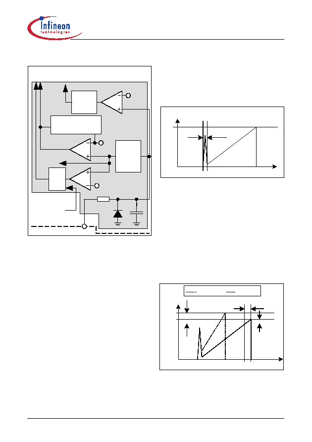
3.2
Power Management
Figure 4
Power Management
The Undervoltage Lockout monitors the external
supply voltage V
VCC
. When the SMPS is plugged to the
main line the internal Startup Cell is biased and starts
to charge the external capacitor C
VCC
which is
connected to the VCC pin. The VCC charge current
that is provided by the Startup Cell from the HV pin is
1.05mA. When V
VCC
exceeds the on-threshold
V
CCon
=15V the internal voltage reference and bias
circuit are switched on. Then the Startup Cell is
switched off by the Undervoltage Lockout and therefore
also the power losses are switched off caused by the
Startup Cell which is connected to the bus voltage
(HV). To avoid uncontrolled ringing at switch-on a
hysteresis is implemented. The switch-off of the
Internal Bias
Voltage
Reference
Power Management
Latched Off Mode
Reset
V
VCC
< 6V
6.5V
Latched Off Mode
Startup Cell
VCC
Undervoltage Lockout
15V
8.5V
HV
T1
Power-Down Reset
SoftS
Active Burst Mode
Auto Restart Mode

F3
ICE3DS01L/LG
Functional Description
Version 2.0 9 15 May 2003
controller can only take place after Active Mode was
entered and V
VCC
falls below 8.5V.
The maximum current consumption before the
controller is activated is about 170
µ
A.
When V
VCC
falls below the off-threshold V
CCoff
=8.5V the
internal reference is switched off and the Power Down
reset let T1 discharging the soft-start capacitor C
SoftS
at
pin SoftS. Thus it is ensured that at every startup cycle
the voltage ramp at pin SoftS starts at zero.
The internal Voltage Reference is switched off if
Latched Off Mode or Auto Restart Mode is entered.
The current consumption is then reduced to 300
µ
A.
When Active Burst Mode is entered the internal Bias is
switched off in order to reduce the current consumption
below 1.1mA while keeping the Voltage Reference still
active as this is necessary in this mode.
In case Latched Off Mode is entered VCC needs to be
lowered below 6V to reset the Latched Off Mode. This
is done usually by disconnecting the SMPS from the
AC line.
3.3
Startup Phase
Figure 5
Soft Start
During the Startup Phase a Soft Start is provided. A
signal V
SoftS
which is generated by the external
capacitor C
Softs
in combination with the internal pull up
resistor R
SoftS
determines the duty cycle until V
SoftS
exceeds 4V.
In the beginning C
SoftS
is immediately charged up to
approx. 1V by T2. Therefore the Soft Start Phase takes
place between 1V and 4V. Above V
SoftsS
= 4V there is
no longer duty cycle limitation DC
max
is controlled by
comparator C7 as comparator C2 blocks the gate G7
(see Figure 6).The maximum charge current in the very
first phase when V
SoftS
is below 1V is limited to 1.9mA.
Figure 6
Startup Phase
By means of this extra charge stage there is no delay
in the beginning of the Startup Phase when there is still
no switching. Furthermore Soft Start is finished at 4V to
have faster the maximum power capability. The duty
cycles DC
1
and DC
2
are depending on the mains and
the primary inductance of the transformer. The
limitation of the primary current by DC
2
is related to
V
SoftS
= 4V. But DC
1
is related to a maximum primary
current which is limited by the internal Current Limiting
with CS = 1V. Therefore the maximum Startup Phase
is divided into a Soft Start Phase until t1 and a phase
from t1 until t2 where maximum power is provided if
demanded by the FB signal.
Soft-Start
Comparator
Soft Start
&
G7
C7
C
SoftS
R
SoftS
T2
3.25k
6.5V
T3
1V
SoftS
Gate Driver
0.85V
x3.7
PWM OP
CS
4V
C2
DC
max
DC
1
DC
2
t
t
V
SoftS
max. Soft Start Phase
1V
4V
5.4V
max. Startup Phase
t1
t2

F3
ICE3DS01L/LG
Functional Description
Version 2.0 10 15 May 2003
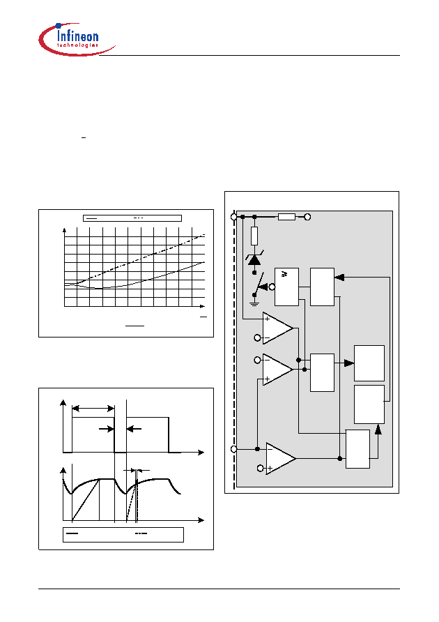
3.4
PWM Section
Figure 7
PWM Section
3.4.1
Oscillator
The oscillator generates a frequency f
switch
= 110kHz. A
resistor, a capacitor and a current source and current
sink which determine the frequency are integrated. The
charging and discharging current of the implemented
oscillator capacitor are internally trimmed, in order to
achieve a very accurate switching frequency. The ratio
of controlled charge to discharge current is adjusted to
reach a maximum duty cycle limitation of D
max
=0.72.
3.4.2
PWM-Latch FF1
The oscillator clock output provides a set pulse to the
PWM-Latch when initiating the external Power Switch
conduction. After setting the PWM-Latch can be reset
by the PWM comparator, the Soft Start comparator, the
Current-Limit comparator or comparator C3. In case of
resetting the driver is shut down immediately.
3.4.3
Gate Driver
The Gate Driver is a fast totem pole gate drive which is
designed to avoid cross conduction currents and which
is equipped with a zener diode Z1 (see Figure 8) in
order to improve the control of the Gate attached power
transistors as well as to protect them against
undesirable gate overvoltages.
The Gate Driver is active low at voltages below the
undervoltage lockout threshold V
VCCoff
.
Figure 8
Gate Driver
The driver-stage is optimized to minimize EMI and to
provide high circuit efficiency. This is done by reducing
the switch on slope when exceeding the external
Power Switch threshold. This is achieved by a slope
control of the rising edge at the driver's output (see
Figure 9).
Figure 9
Gate Rising Slope
Thus the leading switch on spike is minimized. When
the external Power Switch is switched off, the falling
shape of the driver is slowed down when reaching 2V
to prevent an overshoot below ground. Furthermore the
driver circuit is designed to eliminate cross conduction
of the output stage.
Oscillator
Duty Cycle
max
Gate Driver
0.72
Clock
&
G9
1
G8
PWM Section
FF1
R
S
Q
Gate
Soft Start
Comparator
PWM
Comparator
Current
Limiting
Comparator
C3
Z1
VCC
1
PWM-Latch
Gate
t
V
Gate
5V
C
Load
= 1nF
ca. t = 130ns
F3
ICE3DS01L/LG
Functional Description
Version 2.0 11 15May 2003
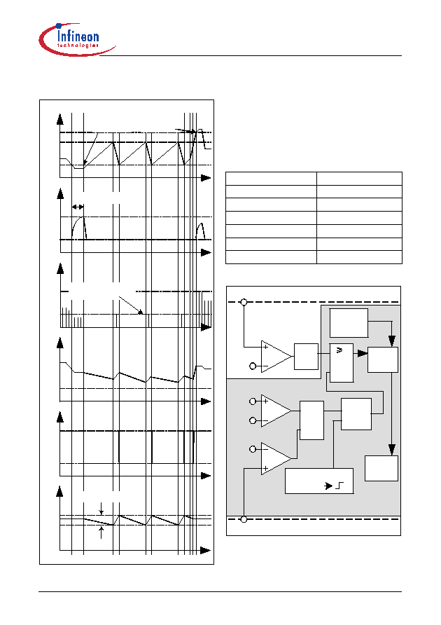
3.5
Current Limiting
Figure 10
Current Limiting
There is a cycle by cycle Current Limiting realized by
the Current-Limit comparator C10 to provide an
overcurrent detection. The source current of the
external Power Switch is sensed via an external sense
resistor R
Sense
. By means of R
Sense
the source current
is transformed to a sense voltage V
Sense
which is fed
into the pin CS. If the voltage V
Sense
exceeds the
internal threshold voltage V
csth
the comparator C10
immediately turns off the gate drive by resetting the
PWM Latch FF1. A Propagation Delay Compensation
is added to support the immediate shut down without
delay of the Power Switch in case of Current Limiting.
The influence of the AC input voltage on the maximum
output power can thereby be avoided.
To prevent the Current Limiting from distortions caused
by leading edge spikes a Leading Edge Blanking is
integrated in the current sense path for the
comparators C10, C12 and the PWM-OP.
A further comparator C11 is implemented to detect
dangerous current levels which could occur if there is a
short winding in the transformer or the secondary diode
is shorten. To ensure that there is no accidentally
entering of the Latched Mode by the comparator C11 a
spike blanking with 190ns is integrated in the output
path of comparator C11.
The output of comparator C12 is activated by the Gate
G10 if Active Burst Mode is entered. Once activated the
current limiting is thereby reduced to 0.257V. This
voltage level determines the power level when the
Active Burst Mode is left if there is a higher power
demand.
3.5.1
Leading Edge Blanking
Figure 11
Leading Edge Blanking
Each time when the external Power Switch is switched
on a leading edge spike is generated due to the
primary-side capacitances and secondary-side rectifier
reverse recovery time. To avoid a premature
termination of the switching pulse this spike is blanked
out with a time constant of t
LEB
= 220ns. During that
time there can't be an accidentally switch off of the gate
drive.
3.5.2
Propagation Delay Compensation
In case of overcurrent detection the shut down of the
external Power Switch is delayed due to the
propagation delay of the circuit. This delay causes an
overshoot of the peak current I
peak
which depends on
the ratio of dI/dt of the peak current (see Figure 12).
Figure 12
Current Limiting
The overshoot of Signal2 is bigger than of Signal1 due
to the steeper rising waveform. This change in the
slope is depending on the AC input voltage.
Propagation Delay Compensation is integrated to limit
C11
Current Limiting
C10
1.66V
C12
&
0.257V
Leading
Edge
Blanking
220ns
G10
Spike
Blanking
190ns
Propagation-Delay
Compensation
V
csth
Active Burst
Mode
PWM Latch
FF1
10k
D1
1pF
PWM-OP
CS
Latched Off
Mode
t
V
Sense
V
csth
t
LEB
= 220ns
t
I
S en s e
I
L im it
t
P rop a g atio n D elay
I
O v e rs ho o t1
I
p e ak 1
S ig n a l1
S ig n a l2
I
O ve rsh o ot2
I
p e ak 2
F3
ICE3DS01L/LG
Functional Description
Version 2.0 12 15 May 2003
the overshoot dependency on dI/dt of the rising primary
current. That means the propagation delay time
between exceeding the current sense threshold V
csth
and the switch off of the external Power Switch is
compensated over temperature within a wide range.
Current Limiting is now possible in a very accurate way
(see Figure 13).
E.g. I
peak
= 0.5A with R
Sense
= 2. Without Propagation
Delay Compensation the current sense threshold is set
to a static voltage level V
csth
=1V. A current ramp of
dI/dt = 0.4A/µs, that means dV
Sense
/dt = 0.8V/µs, and a
propagation delay time of i.e. t
Propagation Delay
=180ns
leads then to an I
peak
overshoot of 12%. By means of
propagation delay compensation the overshoot is only
about 2% (see Figure 13).
Figure 13
Overcurrent Shutdown
The Propagation Delay Compensation is realized by
means of a dynamic threshold voltage V
csth
(see Figure
14). In case of a steeper slope the switch off of the
driver is earlier to compensate the delay.
Figure 14
Dynamic Voltage Threshold V
csth
3.6
Control Unit
The Control Unit contains the functions for Active Burst
Mode, Auto Restart Mode and Latched Off Mode. The
Active Burst Mode and the Auto Restart Mode are
combined with an Adjustable Blanking Window which is
depending on the external Soft Start capacitor. By
means of this Adjustable Blanking Window an
accidentally entering of the Active Burst Mode is
avoided. Furthermore the overload detection can be
deactivated for a certain time.
3.6.1
Adjustable Blanking Window
Figure 15
Adjustable Blanking Window
V
SoftS
is clamped at 4.4V by the closed switch S1 after
the SMPS is settled. If overload occurs V
FB
is
exceeding 4.8V. Auto Restart Mode can't be entered as
the gate G5 is still blocked by the comparator C3. But
after V
FB
has exceeded 4.8V the switch S1 is opened
via the gate G2. The external Soft Start capacitor can
now be charged further by the integrated pull up
resistor R
SoftS
. The comparator C3 releases the gates
0,9
0,95
1
1,05
1,1
1,15
1,2
1,25
1,3
0
0,2
0,4
0,6
0,8
1
1,2
1,4
1,6
1,8
2
with compensation
without compensation
dt
dV
Sense
s
V
µ
Se
ns
e
V
V
t
V
c s th
V
O S C
S ig n a l1
S ig n a l2
V
S e n s e
P ro p a g a tio n D e la y
m a x. D u ty C yc le
o ff tim e
t
C3
5.4V
C4
4.8V
C6
1.32V
&
G5
&
G6
4.4V
S1
&
G4
1
G2
Control Unit
5k
Active
Burst
Mode
Auto
Restart
Mode
R
SoftS
6.5V
SoftS
FB

F3
ICE3DS01L/LG
Functional Description
Version 2.0 13 15 May 2003
G5 and G6 once V
Softs
has exceeded 5.4V. Therefore
there is no entering of Auto Restart Mode possible
during this charging time of the external capacitor
C
SoftS
. The same procedure happens to the external
Soft Start capacitor if a low load condition is detected
by comparator C6 when V
FB
is falling below 1.32V.
Only after V
SoftS
has exceeded 5.4V and V
FB
is still
below 1.32V Active Burst Mode is entered. Once Active
Burst Mode is entered gate G4 is blocked to ensure
that the blanking window is only active before entering
the Active Burst Mode.
3.6.2
Active Burst Mode
The controller provides Active Burst Mode for low load
conditions at V
OUT
. Active Burst Mode increases
significantly the efficiency at light load conditions while
supporting a low ripple on V
OUT
and fast response on
load jumps. During Active Burst Mode which is
controlled only by the FB signal the IC is always active
and can therefore immediately response on fast
changes at the FB signal. The Startup Cell is kept
switched off to avoid increased power losses for the
self supply.
Figure 16
Active Burst Mode
The Active Burst Mode is located in the Control Unit.
Figure 16 shows the related components.
3.6.2.1
Entering Active Burst Mode
The FB signal is always observed by the comparator
C6 if the voltage level falls below 1.32V. In that case the
switch S1 is released which allows the capacitor C
SoftS
to be charged starting from the clamped voltage level
at 4.4V in normal operating mode. The gate G11 is
blocked before entering Active Burst Mode. If V
SoftS
exceeds 5.4V the comparator C3 releases the gate G6
to enter the Active Burst Mode. The time window that is
generated by combining the FB and SoftS signals with
gate G6 avoids a sudden entering of the Active Burst
Mode due to large load jumps. This time window can be
adjusted by the external capacitor C
SoftS
.
After entering Active Burst Mode a burst flag is set
which blocks the gate G4 and the internal bias is
switched off in order to reduce the current consumption
of the IC down to ca. 1.1mA. In this Off State Phase the
IC is no longer self supplied so that therefore C
VCC
has
to provide the VCC current (see Figure 17).
Furthermore gate G11 is then released to start the next
burst cycle once 1.32V is again exceeded.
It has to be ensured by the application that the VCC
remains above the Undervoltage Lockout Level of 8.5V
to avoid that the Startup Cell is accidentally switched
on. Otherwise power losses are significantly increased.
The minimum VCC level during Active Burst Mode is
depending on the load conditions and the application.
The lowest VCC level is reached at no load conditions
at V
OUT
.
3.6.2.2
Working in Active Burst Mode
After entering the Active Burst Mode the FB voltage
rises as V
OUT
starts to decrease due to the inactive
PWM section. Comparator C5 observes the FB signal
if the voltage level 4V is exceeded. In that case the
internal circuit is again activated by the internal Bias to
start with switching. As now in Active Burst Mode the
gate G10 is released the current limit is only 0.257V to
reduce the conduction losses and to avoid audible
noise. If the load at V
OUT
is still below the starting level
for the Active Burst Mode the FB signal decreases
down to 1.32V. At this level C6 deactivates again the
internal circuit by switching off the internal Bias. The
gate G11 is released as after entering Active Burst
Mode the burst flag is set. If working in Active Burst
Mode the FB voltage is changing like a saw tooth
between 1.32V and 4V (see figure 17).
3.6.2.3
Leaving Active Burst Mode
The FB voltage immediately increases if there is a high
load jump. This is observed by comparator C4. As the
current limit is ca. 26% during Active Burst Mode a
certain load jump is needed that FB can exceed 4.8V.
At this time C4 resets the Active Burst Mode which also
C3
5.4V
C4
4.8V
C6
1.32V
C5
4.0V
&
&
G4
FB
Control Unit
Active
Burst
Mode
4.4V
S1
5k
Internal Bias
R
SoftS
6.5V
SoftS
G6
&
G11
&
G10
Current
Limiting
F3
ICE3DS01L/LG
Functional Description
Version 2.0 14 15 May 2003
blocks C12 by the gate G10. Maximum current can now
be provided to stabilize V
OUT
.
Figure 17
Signals in Active Burst Mode
3.6.3
Protection Modes
The IC provides several protection features which are
separated into two categories. Some enter Latched Off
Mode, the others enter Auto Restart Mode. The
Latched Off Mode can only be reset if VCC is falling
below 6V. Both modes prevent the SMPS from
destructive states. The following table shows the
relationship between possible system failures and the
chosen protection modes.
3.6.3.1
Latched Off Mode
Figure 18
Latched Off Mode
The VCC voltage is observed by comparator C1 if 21V
is exceeded. The output of C1 is combined with the
output of C4 which observes FB signal if 4.8V is
1.32V
4.00V
4.80V
V
FB
4.40V
5.40V
V
SoftS
t
t
0.257V
1.00V
V
CS
8.5V
V
VCC
t
t
1.1mA
I
VCC
t
7.2mA
V
OUT
t
Max. Ripple < 1%
Blanking Window
Entering Active
Burst Mode
Leaving Active
Burst Mode
Current limit level during
Active Burst Mode
VCC Overvoltage
Latched Off Mode
Overtemperature
Latched Off Mode
Short Winding/Short Diode
Latched Off Mode
Overload
Auto Restart Mode
Open Loop
Auto Restart Mode
VCC Undervoltage
Auto Restart Mode
Short Optocoupler
Auto Restart Mode
C1
21V
Spike
Blanking
8.0us
&
G1
1
G3
Thermal Shutdown
T
j
>140∞C
Latched
Off Mode
VCC
C4
4.8V
FB
C11
1.66V
Spike
Blanking
190ns
CS
Voltage
Reference
Control Unit
Latched Off
Mode Reset
V
VCC
< 6V

F3
ICE3DS01L/LG
Functional Description
Version 2.0 15 15 May 2003
exceeded. Therefore the overvoltage detection is only
activated if the FB signal is outside the operating range
> 4.8V, e.g. when Open Loop happens. Therewith
small voltage overshoots of V
VCC
during normal
operating can not start the Latched Off Mode.
The internal Voltage Reference is switched off once
Latched Off Mode is entered in order to reduce the
current consumption of the IC as much as possible.
Latched Off Mode can only be reset by decreasing
V
VCC
< 6V. In this stage only the UVLO is working which
controls the Startup Cell by switching on/off at V
VCCon
/
V
VCCoff
. In this phase the average current consumption
is only 300
µ
A. As there is no longer a self supply by the
auxiliary winding VCC drops. The Undervoltage
Lockout switches on the integrated Startup Cell when
VCC falls below 8.5V. The Startup Cell is switched off
again when VCC has exceeded 15V. As the Latched
Off Mode was entered there is no Start Up Phase after
VCC has exceeded the switch-on level of the
Undervoltage Lockout. Therefore VCC changes
between the switch-on and switch-off levels of the
Undervoltage Lockout with a saw tooth shape (see
Figure 19).
Figure 19
Signals in Latched Off Mode
After detecting a junction temperature higher than
140∞C Latched Off Mode is entered.
The signals coming from the temperature detection and
VCC overvoltage detection are fed into a spike
blanking with a time constant of 8.0
µ
s to ensure system
reliability.
Furthermore short winding and short diode on the
secondary side can be detected by the comparator C11
which is in parallel to the propagation delay
compensated current limit comparator C10. In normal
operating mode comparator C10 keeps the maximum
level of the CS signal at 1V. If there is a failure such as
short winding or short diode C10 is no longer able to
limit the CS signal at 1V. C11 detects then the over
current and enters immediately the Latched Off Mode
to keep the SMPS in a safe stage.
3.6.3.2
Auto Restart Mode
Figure 20
Auto Restart Mode
In case of Overload or Open Loop FB exceeds 4.8V
which will be observed by C4. At this time S1 is
released that V
SoftS
can increase. If V
SoftS
exceeds 5.4V
which is observed by C3 Auto Restart Mode is entered
as both inputs of the gate G5 are high. In combining the
FB and SoftS signals there is a blanking window
generated which prevents the system to enter Auto
Restart Mode due to large load jumps. This time
window is the same as for the Active Burst Mode and
can therefore be adjusted by the external C
SoftS
.
In case of VCC undervoltage the UVLO starts a new
startup cycle.
Short Optocoupler leads to VCC undervoltage as there
is now self supply after activating the internal reference
and bias.
In contrast to the Latched Off Mode there is always a
Startup Phase with switching cycles in Auto Restart
Mode. After this Start Up Phase the conditions are
again checked whether the failure is still present.
Normal operation is proceeded once the failure mode
is removed that leads to Auto Restart Mode.
8.5V
t
I
VCCStart
t
1.05mA
V
OUT
V
VCC
15V
C3
5.4V
C4
4.8V
&
G5
4.4V
S1
1
G2
Control Unit
5k
Auto
Restart
Mode
R
SoftS
6.5V
SoftS
FB
Voltage
Reference

F3
ICE3DS01L/LG
Electrical Characteristics
Version 2.0 16 15 May 2003
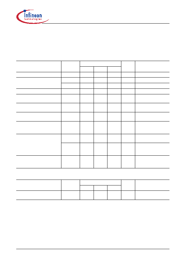
4
Electrical Characteristics
Note:
All voltages are measured with respect to ground (Pin 8). The voltage levels are valid if other ratings are
not violated.
4.1
Absolute Maximum Ratings
Note:
Absolute maximum ratings are defined as ratings, which when being exceeded may lead to destruction
of the integrated circuit. For the same reason make sure, that any capacitor that will be connected to pin 7
(
V
CC) is discharged before assembling the application circuit.
4.2
Operating Range
Note:
Within the operating range the IC operates as described in the functional description.
Parameter
Symbol
Limit Values
Unit
Remarks
min.
max.
HV Voltage
V
HV
-
500V
V
VCC Supply Voltage
V
VCC
-0.3
22
V
FB Voltage
V
FB
-0.3
6.5
V
SoftS Voltage
V
SoftS
-0.3
6.5
V
Gate Voltage
V
Gate
-0.3
22
V
Internally clamped at 11.5V
CS Voltage
V
CS
-0.3
6.5
V
Junction Temperature
T
j
-40
150
∞
C
Storage Temperature
T
S
-55
150
∞
C
Total Power Dissipation
P
totDSO8
-
0.45
W
P-DSO-8-8, T
amb
< 50∞C
P
totDIP8
-
0.90
W
P-DIP-8-6, T
amb
< 50∞C
Thermal Resistance
Junction-Ambient
R
thJADSO8
-
185
K/W
P-DSO-8-8
R
thJADIP8
-
90
K/W
P-DIP-8-6
ESD Capability (incl. Pin HV)
V
ESD
-
3
kV
Human body model
1)
1)
According to EIA/JESD22-A114-B (discharging a 100pF capacitor through a 1.5k
series resistor)
Parameter
Symbol
Limit Values
Unit
Remarks
min.
max.
VCC Supply Voltage
V
VCC
V
VCCoff
20
V
Junction Temperature of
Controller
T
jCon
-25
130
∞C
Max value limited due to thermal
shut down of controller
F3
ICE3DS01L/LG
Electrical Characteristics
Version 2.0 17 15 May 2003
4.3
Characteristics
4.3.1
Supply Section
Note:
The electrical characteristics involve the spread of values guaranteed within the specified supply voltage
and junction temperature range
T
J
from ≠ 25
∞
C to 130
∞
C. Typical values represent the median values,
which are related to 25∞C. If not otherwise stated, a supply voltage of
V
CC
= 15 V is assumed.
4.3.2
Internal Voltage Reference
Parameter
Symbol
Limit Values
Unit
Test Condition
min.
typ.
max.
Start Up Current
I
VCCstart
-
170
220
µ
A
V
VCC
=14V
VCC Charge Current
I
VCCcharge1
-1.60
-1.05
-0.55
mA
V
VCC
= 0V
I
VCCcharge2
-
-0.88
-
mA
V
VCC
=14V
Start Up Cell Leakage Current
I
StartLeak
-
2
20
µ
A
V
VCC
>16V
Supply Current with Inactive
Gate
I
VCCsup1
-
6.0
7.5
mA
Supply Current with Active Gate
(C
Load
=1nF)
I
VCCsup2
-
7.2
8.7
mA
V
SoftS
= 4.4V
I
FB
= 0
Supply Current in
Latched Off Mode
I
VCClatch
-
300
-
µ
A
I
FB
= 0
I
Softs
= 0
Supply Current in
Auto Restart Mode
with Inactive Gate
I
VCCrestart
-
300
-
µ
A
I
FB
= 0
I
Softs
= 0
Supply Current in
Active Burst Mode
with Inactive Gate
I
VCCburst1
-
1.1
1.3
mA
V
FB
= 2.5V
V
SoftS
= 4.4V
I
VCCburst2
-
1.0
1.2
mA
V
VCC
= 9V
V
FB
= 2.5V
V
SoftS
= 4.4V
VCC Turn-On Threshold
VCC Turn-Off Threshold
VCC Turn-On/Off Hysteresis
V
VCCon
V
VCCoff
V
VCChys
14.2
8.0
-
15.0
8.5
6.5
15.8
9.0
-
V
V
V
Parameter
Symbol
Limit Values
Unit
Test Condition
min.
typ.
max.
Trimmed Reference Voltage
V
REF
6.37
6.50
6.63
V
measured at pin FB
I
FB
= 0

F3
ICE3DS01L/LG
Electrical Characteristics
Version 2.0 18 15 May 2003
4.3.3
PWM Section
4.3.4
Control Unit
Note:
The trend of all the voltage levels in the Control Unit is the same regarding the deviation except V
VCCOVP
and V
VCCPD
Parameter
Symbol
Limit Values
Unit
Test Condition
min.
typ.
max.
Fixed Oscillator Frequency
f
OSC1
98
110
119
kHz
f
OSC2
102
110
117
kHz
T
j
= 25∞C
Max. Duty Cycle
D
max
0.67
0.72
0.77
Min. Duty Cycle
D
min
0
-
-
V
FB
< 0.3V
PWM-OP Gain
A
V
3.5
3.7
3.9
Max. Level of Voltage Ramp
V
Max-Ramp
-
0.85
-
V
V
FB
Operating Range Min Level
V
FBmin
0.3
0.7
-
V
V
FB
Operating Range Max level
V
FBmax
-
-
4.75
V
CS=1V limited by
Comparator C4
1)
1)
Design characteristic (not meant for production testing)
Feedback Pull-Up Resistor
R
FB
16
20
27
k
Soft-Start Pull-Up Resistor
R
SoftS
39
50
62
k
Parameter
Symbol
Limit Values
Unit
Test Condition
min.
typ.
max.
Deactivation Level for SoftS
Comparator C7 by C2
V
SoftSC2
3.85
4.00
4.15
V
V
FB
> 5V
Clamped V
SoftS
Voltage during
Normal Operating Mode
V
SoftSclmp
4.23
4.40
4.57
V
V
FB
< 4.5V
Activation Limit of
Comparator C3
V
SoftSC3
5.20
5.40
5.60
V
V
FB
> 5V
SoftS Startup Current
I
SoftSstart
-
1.9
-
mA
V
SoftS
= 0V
Active Burst Mode Level for
Comparator C6
V
FBC6
1.23
1.32
1.40
V
V
SoftS
> 5.6V
Active Burst Mode Level for
Comparator C5
V
FBC5
3.85
4.00
4.15
V
After Active Burst
Mode is entered
Over Load & Open Loop
Detection Limit for
Comparator C4
V
FBC4
4.62
4.80
4.98
V
V
SoftS
> 5.6V
Overvoltage Detection Limit
V
VCCOVP
20
21
22
V
V
FB
> 5V
Latched Thermal Shutdown
T
jSD
130
140
150
∞C
guaranteed by design
Spike Blanking
t
Spike
-
8.0
-
µ
s
Power Down Reset for Latched
Mode
V
VCCPD
4.0
6.0
7.5
V
After Latched Off Mode
is entered

F3
ICE3DS01L/LG
Electrical Characteristics
Version 2.0 19 15 May 2003
4.3.5
Current Limiting
4.3.6
Driver Section
Parameter
Symbol
Limit Values
Unit
Test Condition
min.
typ.
max.
Peak Current Limitation (incl.
Propagation Delay Time)
(see Figure 7)
V
csth
0.950
1.000
1.050
V
dV
sense
/ dt = 0.6V/
µ
s
Over Current Detection for
Latched Off Mode
V
CS1
1.570
1.66
1.764
V
Peak Current Limitation during
Active Burst Mode
V
CS2
0.232
0.257
0.282
V
V
FB
< 1.2V
Leading Edge Blanking
t
LEB
-
220
-
ns
V
SoftS
= 4.4V
CS Spike Blanking for
Comparator C11
t
CSspike
-
190
-
ns
CS Input Bias Current
I
CSbias
-1.0
-0.2
0
µ
A
V
CS
=0V
Parameter
Symbol
Limit Values
Unit
Test Condition
min.
typ.
max.
GATE Low Voltage
V
GATElow
-
-
1.2
V
V
VCC
= 5 V
I
Gate
= 5 mA
-
-
1.5
V
V
VCC
= 5 V
I
Gate
= 20 mA
-
0.8
-
V
I
Gate
= 0 A
-
1.6
2.0
V
I
Gate
= 20 mA
-0.2
0.2
-
V
I
Gate
= -20 mA
GATE High Voltage
V
GATEhigh
-
11.5
-
V
V
VCC
= 20V
C
L
= 4.7nF
-
10.5
-
V
V
VCC
= 11V
C
L
= 4.7nF
-
7.5
-
V
V
VCC
= V
VCCoff
+ 0.2V
C
L
= 4.7nF
GATE Rise Time
(incl. Gate Rising Slope)
t
rise
-
150
-
ns
V
Gate
= 2V ...9V
1)
C
L
= 4.7nF
1)
Transient reference value
GATE Fall Time
t
fall
-
55
-
ns
V
Gate
= 9V ...2V
1)
C
L
= 4.7nF
GATE Current, Peak,
Rising Edge
I
GATE
-0.5
-
-
A
C
L
= 4.7nF
2)
2)
Design characteristic (not meant for production testing)
GATE Current, Peak,
Falling Edge
I
GATE
-
-
0.7
A
C
L
= 4.7nF
2)

Version 2.0 20 15 May 2003
F3
ICE3DS01L/LG
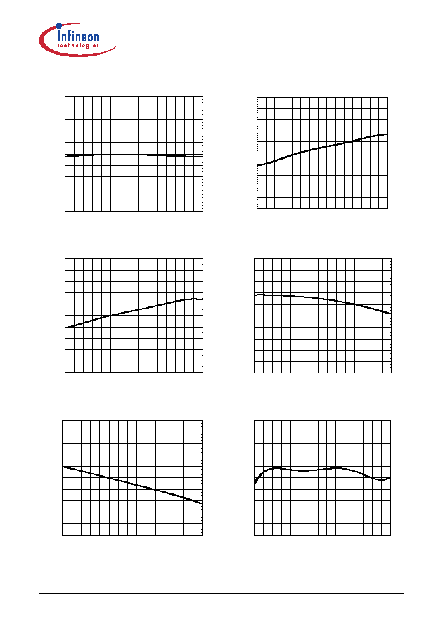
Typical Performance Characteristics
5
Typical Performance Characteristics
Figure 21
Start Up Current I
VCCstart
Figure 22
VCC Charge Current I
VCCcharge1
Figure 23
VCC Charge Current I
VCCcharge2
Figure 24
VCC Supply Current I
VCCsup1
Figure 25
VCC Supply Current I
VCCsup2
Figure 26 VCC Supply Current I
VCClatch
Junction Temperature [∞C]
St
ar
t
Up
Cu
r
r
e
n
t
I
VCCstart
[uA
]
P
I
-
001
150
154
158
162
166
170
174
178
182
186
190
-25 -15
-5
5
15
25
35
45
55
65
75
85
95 105 115 125
Junction Temperature [∞C]
VCC Cha
rge
Curre
nt I
V
CCcharge1
[mA]
P
I
-
002
0,5
0,6
0,7
0,8
0,9
1,0
1,1
1,2
1,3
1,4
1,5
-25 -15
-5
5
15
25
35
45
55
65
75
85
95 105 115 125
Junction Temperature [∞C]
VCC Ch
a
r
g
e
Cu
r
r
e
n
t
I
VCCch
a
rg
e2
[m
A
]
P
I
-
003
0,5
0,6
0,7
0,8
0,9
1,0
1,1
1,2
1,3
1,4
1,5
-25 -15
-5
5
15
25
35
45
55
65
75
85
95 105 115 125
Junction Temperature [∞C]
VC
C
Supply C
u
rrent I
V
CCsup1
[mA
]
P
I
-
004
3,0
3,5
4,0
4,5
5,0
5,5
6,0
6,5
7,0
7,5
8,0
-25 -15
-5
5
15
25
35
45
55
65
75
85
95 105 115 125
Junction Temperature [∞C]
VCC Supply Current I
V
CCsup2
[mA]
P
I
-
005
4,0
4,5
5,0
5,5
6,0
6,5
7,0
7,5
8,0
8,5
9,0
-25 -15
-5
5
15
25
35
45
55
65
75
85
95 105 115 125
Junction Temperature [∞C]
VC
C
Supply C
urrent I
V
CClat
ch
[uA
]
P
I
-
006
200
220
240
260
280
300
320
340
360
380
400
-25 -15
-5
5
15
25
35
45
55
65
75
85
95 105 115 125

F3
ICE3DS01L/LG
Typical Performance Characteristics
Version 2.0 21 15 May 2003
Figure 27
VCC Supply Current I
VCCrestart
Figure 28
VCC Supply Current I
VCCburst1
Figure 29
VCC Supply Current I
VCCburst2
Figure 30
VCC Turn-On Threshold V
VCCon
Figure 31
VCC Turn-Off Threshold V
VCCoff
Figure 32
VCC Turn-On/Off Hysteresis V
VCChys
Junction Temperature [∞C]
VCC Supply Current I
V
CCrest
art
[uA]
P
I
-
007
200
220
240
260
280
300
320
340
360
380
400
-25 -15
-5
5
15
25
35
45
55
65
75
85
95 105 115 125
Junction Temperature [∞C]
VC
C
Supply C
u
rrent I
V
CCburst
1
[mA
]
P
I
-
008
0,90
0,93
0,96
0,99
1,02
1,05
1,08
1,11
1,14
1,17
1,20
-25 -15
-5
5
15
25
35
45
55
65
75
85
95 105 115 125
Junction Temperature [∞C]
VCC Supply Current I
VCCb
u
r
st
2
[mA]
P
I
-
009
0,90
0,93
0,96
0,99
1,02
1,05
1,08
1,11
1,14
1,17
1,20
-25 -15
-5
5
15
25
35
45
55
65
75
85
95 105 115 125
Junction Temperature [∞C]
VC
C
Turn-On Threshold V
V
CCon
[V]
P
I
-
010
14,0
14,2
14,4
14,6
14,8
15,0
15,2
15,4
15,6
15,8
16,0
-25 -15
-5
5
15
25
35
45
55
65
75
85
95 105 115 125
Junction Temperature [∞C]
VC
C
Turn-Off Threshold V
V
CCof
f
[V]
P
I
-
011
8,0
8,1
8,2
8,3
8,4
8,5
8,6
8,7
8,8
8,9
9,0
-25 -15
-5
5
15
25
35
45
55
65
75
85
95 105 115 125
Junction Temperature [∞C]
VCC Turn-On/Off Hysteresis V
V
CChys
[V]
P
I
-
012
6,0
6,1
6,2
6,3
6,4
6,5
6,6
6,7
6,8
6,9
7,0
-25 -15
-5
5
15
25
35
45
55
65
75
85
95 105 115 125

F3
ICE3DS01L/LG
Typical Performance Characteristics
Version 2.0 22 15 May 2003
Figure 33
Reference Voltage V
REF
Figure 34
Oscillator Frequency f
OSC1
Figure 35
Max. Duty Cycle D
max
Figure 36
PWM-OP Gain A
V
Figure 37
Max. Level Voltage Ramp V
Max-Ramp
Figure 38
Feedback Pull-Up Resistor R
FB
Junction Temperature [∞C]
Refer
e
nce V
o
ltage V
RE
F
[V
]
P
I
-
013
6,40
6,42
6,44
6,46
6,48
6,50
6,52
6,54
6,56
6,58
6,60
-25 -15
-5
5
15
25
35
45
55
65
75
85
95 105 115 125
Junction Temperature [∞C]
Oscillator Frequency f
OS
C
1
[kH
z
]
P
I
-
014
100
102
104
106
108
110
112
114
116
118
120
-25 -15
-5
5
15
25
35
45
55
65
75
85
95 105 115 125
Junction Temperature [∞C]
Max. Duty Cycle
P
I
-
015
0,700
0,705
0,710
0,715
0,720
0,725
0,730
0,735
0,740
0,745
0,750
-25 -15
-5
5
15
25
35
45
55
65
75
85
95 105 115 125
Junction Temperature [∞C]
P
W
M-OP
Gain A
V
P
I
-
016
3,50
3,54
3,58
3,62
3,66
3,70
3,74
3,78
3,82
3,86
3,90
-25 -15
-5
5
15
25
35
45
55
65
75
85
95 105 115 125
Junction Temperature [∞C]
Max. Level V
o
ltage Ram
p
V
M
ax-
Ramp
[V
]
P
I
-
017
0,60
0,65
0,70
0,75
0,80
0,85
0,90
0,95
1,00
1,05
1,10
-25 -15
-5
5
15
25
35
45
55
65
75
85
95 105 115 125
Junction Temperature [∞C]
Feedback Pull-U
p
R
esistor R
FB
[kOhm]
P
I
-
018
16
17
18
19
20
21
22
23
24
25
26
-25 -15
-5
5
15
25
35
45
55
65
75
85
95 105 115 125

F3
ICE3DS01L/LG
Typical Performance Characteristics
Version 2.0 23 15 May 2003
Figure 39
Soft-Start Pull-Up Resistor R
SoftS
Figure 40
Threshold Comparator C2 V
SoftSC2
Figure 41
Clamped SoftS Voltage V
SoftSclmp
Figure 42
Threshold Comparator C3 V
SoftSC3
Figure 43
Threshold Comparator C6 V
FBC6
Figure 44
Threshold Comparator C5 V
FBC5
Junction Temperature [∞C]
Soft-Start Pull-U
p
R
esistor R
SoftS
[kOhm]
P
I
-
019
40
42
44
46
48
50
52
54
56
58
60
-25 -15
-5
5
15
25
35
45
55
65
75
85
95 105 115 125
Junction Temperature [∞C]
Thr
eshold C
o
m
p
ar
ator
C
2
V
SoftSC
2
[V
]
P
I
-
020
3,80
3,84
3,88
3,92
3,96
4,00
4,04
4,08
4,12
4,16
4,20
-25 -15
-5
5
15
25
35
45
55
65
75
85
95 105 115 125
Junction Temperature [∞C]
C
l
amped SoftS Voltage V
S
o
ftS
c
l
m
p
[V]
P
I
-
021
4,20
4,24
4,28
4,32
4,36
4,40
4,44
4,48
4,52
4,56
4,60
-25 -15
-5
5
15
25
35
45
55
65
75
85
95 105 115 125
Junction Temperature [∞C]
Threshold Comparator C3 V
SoftSC
3
[V]
P
I
-
022
5,15
5,20
5,25
5,30
5,35
5,40
5,45
5,50
5,55
5,60
5,65
-25 -15
-5
5
15
25
35
45
55
65
75
85
95 105 115 125
Junction Temperature [∞C]
Threshold C
omparator C
6
V
FBC6
[V]
P
I
-
023
1,280
1,288
1,296
1,304
1,312
1,320
1,328
1,336
1,344
1,352
1,360
-25 -15
-5
5
15
25
35
45
55
65
75
85
95 105 115 125
Junction Temperature [∞C]
Threshold C
o
mparator C
5
V
FBC5
[V]
PI-0
2
4
3,80
3,84
3,88
3,92
3,96
4,00
4,04
4,08
4,12
4,16
4,20
-25 -15
-5
5
15
25
35
45
55
65
75
85
95 105 115 125
F3
ICE3DS01L/LG
Typical Performance Characteristics
Version 2.0 24 15 May 2003
Figure 45
Threshold Comparator C4 V
FBC4
Figure 46
Overvoltage Detection Limit V
VCCOVP
Figure 47
Threshold Power Down Reset V
VCCPD
Figure 48
Peak Current Limitation V
csth
Figure 49
Over Current Detection V
CS1
Figure 50
Peak Current Limitation V
CS2
Junction Temperature [∞C]
Thr
eshold C
o
m
p
ar
ator
C
4
V
F
BC4
[V
]
P
I
-
025
4,60
4,64
4,68
4,72
4,76
4,80
4,84
4,88
4,92
4,96
5,00
-25 -15
-5
5
15
25
35
45
55
65
75
85
95 105 115 125
Junction Temperature [∞C]
O
ver
vo
lt
ag
e Det
ect
io
n
L
i
mit
V
VCCO
VP
[V
]
P
I
-
026
20,0
20,2
20,4
20,6
20,8
21,0
21,2
21,4
21,6
21,8
22,0
-25 -15
-5
5
15
25
35
45
55
65
75
85
95 105 115 125
Junction Temperature [∞C]
V
CC P
o
wer
Down Reset V
V
CCP
D
[V
]
P
I
-
027
4,0
4,4
4,8
5,2
5,6
6,0
6,4
6,8
7,2
7,6
8,0
-25 -15
-5
5
15
25
35
45
55
65
75
85
95 105 115 125
Junction Temperature [∞C]
Peak Current Limitation V
csth
[V]
PI-
0
28
0,95
0,96
0,97
0,98
0,99
1,00
1,01
1,02
1,03
1,04
1,05
-25 -15 -5
5 15 25 35 45 55 65 75 85 95 105 115 125
Junction Temperature [∞C]
Over Current Detection V
CS
1
[V
]
P
I
-
029
1,580
1,592
1,604
1,616
1,628
1,640
1,652
1,664
1,676
1,688
1,700
-25 -15
-5
5
15
25
35
45
55
65
75
85
95 105 115 125
Junction Temperature [∞C]
P
eak Cur
r
ent Limitation V
CS
2
[V
]
P
I
-
030
0,240
0,243
0,246
0,249
0,252
0,255
0,258
0,261
0,264
0,267
0,270
-25 -15
-5
5
15
25
35
45
55
65
75
85
95 105 115 125

F3
ICE3DS01L/LG
Typical Performance Characteristics
Version 2.0 25 15 May 2003
Figure 51
Leading Edge Blanking t
LEB
Figure 52
CS Spike Blanking for C11 t
CSspike
Figure 53
GATE Low Voltage V
GATElow
Figure 54
GATE High Voltage V
GATEhigh
Figure 55
GATE Rise Time t
rise
Figure 56
GATE Fall Time t
fall
Junction Temperature [∞C]
Leading Edge B
l
anking t
LE
B
[ns]
P
I
-
031
100
130
160
190
220
250
280
310
340
370
400
-25 -15
-5
5
15
25
35
45
55
65
75
85
95 105 115 125
Junction Temperature [∞C]
CS
S
p
ike Blanking for
C11 t
CS
sp
i
ke
[ns]
P
I
-
032
100
120
140
160
180
200
220
240
260
280
300
-25 -15
-5
5
15
25
35
45
55
65
75
85
95 105 115 125
Junction Temperature [∞C]
GA
TE
Low V
o
l
t
age V
GA
TE
low
[V
]
P
I
-
033
0,3
0,4
0,5
0,6
0,7
0,8
0,9
1,0
1,1
1,2
1,3
-25 -15
-5
5
15
25
35
45
55
65
75
85
95 105 115 125
Junction Temperature [∞C]
Gate High V
o
ltage V
GA
TE
high
[V
]
P
I
-
034
9,0
9,3
9,6
9,9
10,2
10,5
10,8
11,1
11,4
11,7
12,0
-25 -15
-5
5
15
25
35
45
55
65
75
85
95 105 115 125
Junction Temperature [∞C]
Gate Rise Time t
r
i
se
[ns]
P
I
-
035
100
120
140
160
180
200
220
240
260
280
300
-25 -15
-5
5
15
25
35
45
55
65
75
85
95 105 115 125
Junction Temperature [∞C]
GA
TE
Fal
l
Ti
m
e
t
f
a
ll
[ns]
P
I
-
036
40
44
48
52
56
60
64
68
72
76
80
-25 -15
-5
5
15
25
35
45
55
65
75
85
95 105 115 125

F3
ICE3DS01L/LG
Outline Dimension
Version 2.0 26 15 May 2003
6
Outline Dimension
Figure 57
Figure 58
Dimensions in mm
P-DIP-8-6
(Plastic Dual In-Line Outline)
P-DSO-8-8
(Plastic Dual Small Outline)

Qualit‰t hat f¸r uns eine umfassende
Bedeutung. Wir wollen allen Ihren
Anspr¸chen in der bestmˆglichen
Weise gerecht werden. Es geht uns also
nicht nur um die Produktqualit‰t ≠
unsere Anstrengungen gelten
gleichermaþen der Lieferqualit‰t und
Logistik, dem Service und Support
sowie allen sonstigen Beratungs- und
Betreuungsleistungen.
Dazu gehˆrt eine bestimmte
Geisteshaltung unserer Mitarbeiter.
Total Quality im Denken und Handeln
gegen¸ber Kollegen, Lieferanten und
Ihnen, unserem Kunden. Unsere
Leitlinie ist jede Aufgabe mit ,,Null
Fehlern" zu lˆsen ≠ in offener
Sichtweise auch ¸ber den eigenen
Arbeitsplatz hinaus ≠ und uns st‰ndig
zu verbessern.
Unternehmensweit orientieren wir uns
dabei auch an ,,top" (Time Optimized
Processes), um Ihnen durch grˆþere
Schnelligkeit den entscheidenden
Wettbewerbsvorsprung zu verschaffen.
Geben Sie uns die Chance, hohe
Leistung durch umfassende Qualit‰t zu
beweisen.
Wir werden Sie ¸berzeugen.
Quality takes on an allencompassing
significance at Semiconductor Group.
For us it means living up to each and
every one of your demands in the best
possible way. So we are not only
concerned with product quality. We
direct our efforts equally at quality of
supply and logistics, service and
support, as well as all the other ways in
which we advise and attend to you.
Part of this is the very special attitude of
our staff. Total Quality in thought and
deed, towards co-workers, suppliers
and you, our customer. Our guideline is
"do everything with zero defects", in an
open manner that is demonstrated
beyond your immediate workplace, and
to constantly improve.
Throughout the corporation we also
think in terms of Time Optimized
Processes (top), greater speed on our
part to give you that decisive
competitive edge.
Give us the chance to prove the best of
performance through the best of quality
≠ you will be convinced.
h t t p : / / w w w . i n f i n e o n . c o m
Total Quality Management
Published by Infineon Technologies AG