
IGP03N120H2, IGB03N120H2
IGW03N120H2
Power Semiconductors
1
Rev. 2, Mar-04
HighSpeed 2-Technology
∑
Designed for:
- SMPS
- Lamp Ballast
- ZVS-Converter
- optimised for soft-switching / resonant topologies
∑
2
nd
generation HighSpeed-Technology
for 1200V applications offers:
- loss reduction in resonant circuits
- temperature stable behavior
- parallel switching capability
- tight parameter distribution
-
E
off
optimized for
I
C
=3A
∑
Complete product spectrum and PSpice Models :
http://www.infineon.com/igbt/
Type
V
CE
I
C
E
off
T
j
Package Ordering
Code
IGW03N120H2 1200V 3A 0.15mJ 150
∞
C
P-TO-247 Q67040-S4596
IGP03N120H2 1200V 3A 0.15mJ 150∞C
P-TO-220-3-1
Q67040-S4599
IGB03N120H2 1200V 3A 0.15mJ 150∞C
P-TO-263
(D
2
PAK) Q67040-S4598
Maximum Ratings
Parameter Symbol
Value
Unit
Collector-emitter voltage
V
C E
1200
V
Triangular collector current
T
C
= 25
∞
C,
f
= 140kHz
T
C
= 100
∞
C,
f
= 140kHz
I
C
9.6
3.9
Pulsed collector current,
t
p
limited by
T
jmax
I
C p u l s
9.9
Turn off safe operating area
V
CE
1200V,
T
j
150
∞
C
-
9.9
A
Gate-emitter voltage
V
G E
±
20
V
Power dissipation
T
C
= 25
∞
C
P
t o t
62.5
W
Operating junction and storage temperature
T
j
,
T
s t g
-40...+150
Soldering temperature, 1.6mm (0.063 in.) from case for 10s
-
260
225 (for SMD)
∞
C
G
C
E
P-TO-220-3-1
(TO-220AB)
P-TO-263-3-2 (D≤-PAK)
(TO-263AB)
P-TO-247-3-1
(TO-247AC)

IGP03N120H2, IGB03N120H2
IGW03N120H2
Power Semiconductors
2
Rev. 2, Mar-04
Thermal Resistance
Parameter Symbol
Conditions
Max.
Value
Unit
Characteristic
IGBT thermal resistance,
junction ≠ case
R
t h J C
2.0
Thermal resistance,
junction ≠ ambient
R
t h J A
P-TO-220-3-1
P-TO-247-3-1
62
SMD version, device on PCB
1)
R
t h J A
P-TO-263
(D
2
PAK) 40
K/W
Electrical Characteristic,
at
T
j
= 25
∞
C, unless otherwise specified
Value
Parameter Symbol
Conditions
min. Typ. max.
Unit
Static Characteristic
Collector-emitter breakdown voltage
V
( B R ) C E S
V
G E
=0V,
I
C
=300
µ
A
1200 -
-
Collector-emitter saturation voltage
V
C E ( s a t )
V
G E
= 15V,
I
C
=3A
T
j
=25
∞
C
T
j
=150
∞
C
V
G E
= 10V,
I
C
=3A,
T
j
=25
∞
C
-
-
-
2.2
2.5
2.4
2.8
-
-
Gate-emitter threshold voltage
V
G E ( t h )
I
C
=90
µ
A,
V
C E
=
V
G E
2.1 3 3.9
V
Zero gate voltage collector current
I
C E S
V
C E
=1200V,
V
G E
=0V
T
j
=25
∞
C
T
j
=150
∞
C
-
-
-
-
20
80
µ
A
Gate-emitter leakage current
I
G E S
V
C E
=0V,
V
G E
=20V
- - 100
nA
Transconductance
g
f s
V
C E
=20V,
I
C
=3A
- 2 -
S
Dynamic Characteristic
Input capacitance
C
i s s
-
205
-
Output capacitance
C
o s s
- 24 -
Reverse transfer capacitance
C
r s s
V
C E
=25V,
V
G E
=0V,
f
=1MHz
- 7 -
pF
Gate charge
Q
G a t e
V
C C
=960V,
I
C
=3A
V
G E
=15V
- 22 -
nC
Internal emitter inductance
measured 5mm (0.197 in.) from case
L
E
P-TO-220-3-1
P-TO-247-3-1
-
7
13
-
nH
1)
Device on 50mm*50mm*1.5mm epoxy PCB FR4 with 6cm
2
(one layer, 70
µ
m thick) copper area for
collector connection. PCB is vertical without blown air.

IGP03N120H2, IGB03N120H2
IGW03N120H2
Power Semiconductors
3
Rev. 2, Mar-04
Switching Characteristic, Inductive Load,
at
T
j
=25
∞
C
Value
Parameter Symbol
Conditions
min. typ. max.
Unit
IGBT Characteristic
Turn-on delay time
t
d ( o n )
-
9.2
-
Rise time
t
r
-
5.2
-
Turn-off delay time
t
d ( o f f )
-
281
-
Fall time
t
f
- 29 -
ns
Turn-on energy
E
o n
-
0.14
-
Turn-off energy
E
o f f
-
0.15
-
Total switching energy
E
t s
T
j
=25
∞
C,
V
C C
=800V,
I
C
=3A,
V
G E
=15V/0V,
R
G
=82
,
L
2 )
=180nH,
C
2 )
=40pF
Energy losses include
"tail" and diode
3)
reverse recovery.
- 0.29 -
mJ
Switching Characteristic, Inductive Load,
at
T
j
=150
∞
C
Value
Parameter Symbol
Conditions
min. typ. max.
Unit
IGBT Characteristic
Turn-on delay time
t
d ( o n )
-
9.4
-
Rise time
t
r
-
6.7
-
Turn-off delay time
t
d ( o f f )
-
340
-
Fall time
t
f
- 63 -
ns
Turn-on energy
E
o n
-
0.22
-
Turn-off energy
E
o f f
-
0.26
-
Total switching energy
E
t s
T
j
=150
∞
C
V
C C
=800V,
I
C
=3A,
V
G E
=15V/0V,
R
G
=82
,
L
2 )
=180nH,
C
2 )
=40pF
Energy losses include
"tail" and diode
3)
reverse recovery.
- 0.48 -
mJ
Switching Energy ZVT, Inductive Load
Value
Parameter Symbol
Conditions
min. typ. max.
Unit
IGBT Characteristic
Turn-off energy
E
o f f
V
C C
=800V,
I
C
=3A,
V
G E
=15V/0V,
R
G
=82
,
C
r
2 )
=4nF
T
j
=25
∞
C
T
j
=150
∞
C
-
-
0.05
0.09
-
-
mJ
2)
Leakage inductance L
and stray capacity C
due to dynamic test circuit in figure E
3)
Commutation diode from device IKP03N120H2

IGP03N120H2, IGB03N120H2
IGW03N120H2
Power Semiconductors
4
Rev. 2, Mar-04
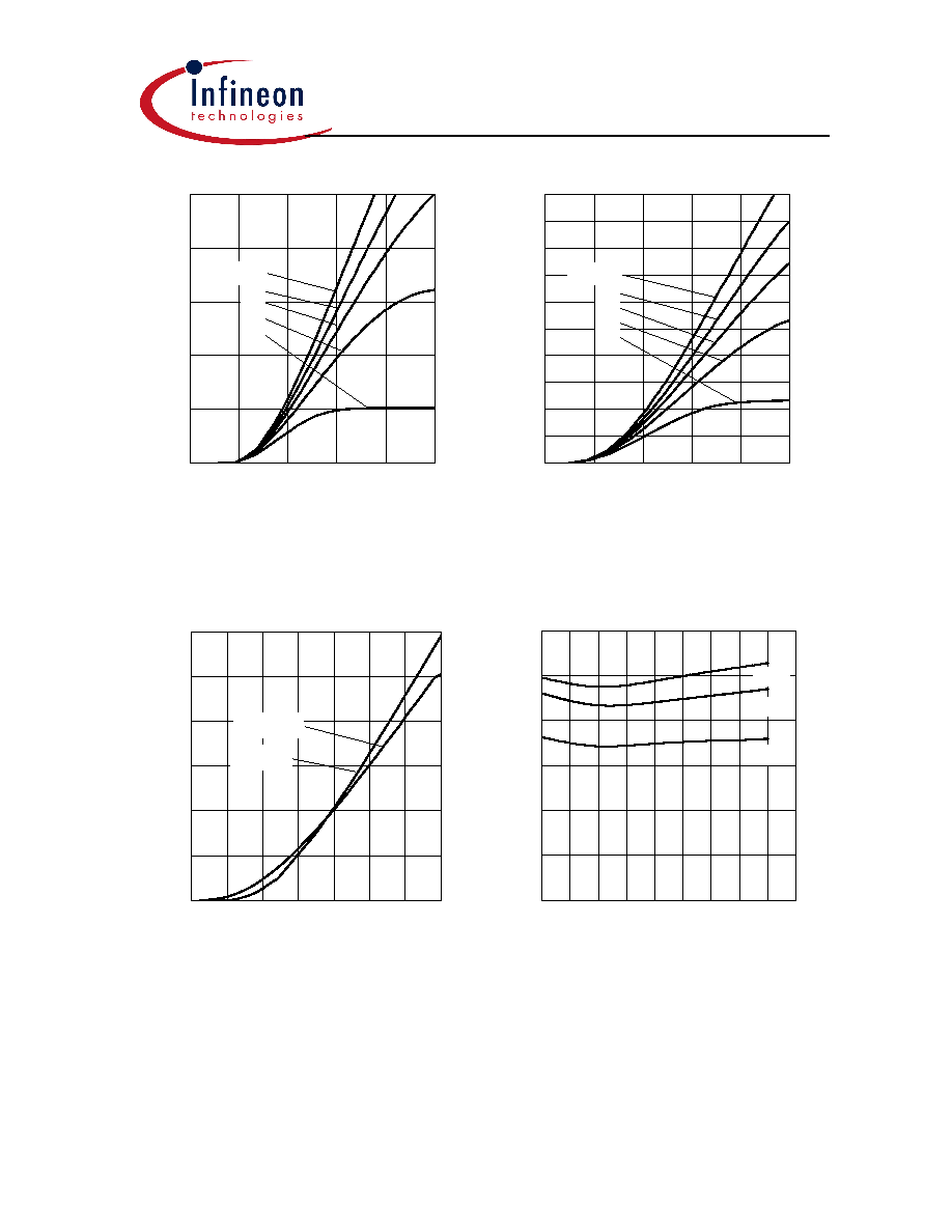
I
C
,
COL
L
E
C
T
O
R C
URR
EN
T
10Hz
100Hz
1kHz
10kHz
100kHz
0A
2A
4A
6A
8A
10A
12A
T
C
=110∞C
T
C
=80∞C
I
C
,
COL
L
E
C
T
O
R C
URR
EN
T
1V
10V
100V
1000V
,01A
0,1A
1A
10A
100
µ
s
DC
500
µ
s
10
µ
s
5
µ
s
50
µ
s
t
p
=1
µ
s
f
,
SWITCHING FREQUENCY
V
CE
,
COLLECTOR
-
EMITTER VOLTAGE
Figure 1. Collector current as a function of
switching frequency
(
T
j
150
∞
C,
D =
0.5,
V
CE
= 800V,
V
GE
= +15V/0V,
R
G
= 82
)
Figure 2. Safe operating area
(
D =
0,
T
C
= 25
∞
C,
T
j
150
∞
C)
P
tot
,
PO
W
E
R
D
I
S
S
I
PATI
O
N
25∞C
50∞C
75∞C
100∞C
125∞C
0W
10W
20W
30W
40W
50W
60W
I
C
,
C
O
LL
EC
T
O
R CU
RR
E
N
T
25∞C
50∞C
75∞C
100∞C
125∞C
150∞C
0A
2A
4A
6A
8A
10A
12A
T
C
,
CASE TEMPERATURE
T
C
,
CASE TEMPERATURE
Figure 3. Power dissipation as a function
of case temperature
(
T
j
150
∞
C)
Figure 4. Collector current as a function of
case temperature
(
V
GE
15V,
T
j
150
∞
C)
I
c
I
c
IGP03N120H2, IGB03N120H2
IGW03N120H2
Power Semiconductors
5
Rev. 2, Mar-04
I
C
,
COL
L
E
C
T
O
R
C
URR
EN
T
0V
1V
2V
3V
4V
5V
0A
2A
4A
6A
8A
10A
12V
10V
8V
6V
V
GE
=15V
I
C
,
COL
L
E
C
T
O
R
C
URR
EN
T
0V
1V
2V
3V
4V
5V
0A
1A
2A
3A
4A
5A
6A
7A
8A
9A
10A
12V
10V
8V
6V
V
GE
=15V
V
CE
,
COLLECTOR
-
EMITTER VOLTAGE
V
CE
,
COLLECTOR
-
EMITTER VOLTAGE
Figure 5. Typical output characteristics
(
T
j
= 25
∞
C)
Figure 6. Typical output characteristics
(
T
j
= 150
∞
C)
I
C
,
COL
L
E
C
T
O
R
C
URR
EN
T
3V
5V
7V
9V
0A
2A
4A
6A
8A
10A
12A
T
j
=+150∞C
T
j
=+25∞C
V
CE
(sat)
,
C
O
LLE
CT
OR
-
E
M
I
T
TE
R SA
TURA
T
I
O
N
VO
LTAGE
-50∞C
0∞C
50∞C
100∞C
150∞C
0V
1V
2V
3V
I
C
=6A
I
C
=3A
I
C
=1.5A
V
GE
,
GATE
-
EMITTER VOLTAGE
T
j
,
JUNCTION TEMPERATURE
Figure 7. Typical transfer characteristics
(
V
CE
= 20V)
Figure 8. Typical collector-emitter
saturation voltage as a function of junction
temperature
(
V
GE
= 15V)

IGP03N120H2, IGB03N120H2
IGW03N120H2
Power Semiconductors
6
Rev. 2, Mar-04
t
,
SWIT
C
H
I
N
G T
I
ME
S
0A
2A
4A
1ns
10ns
100ns
1000ns
t
r
t
d(on)
t
f
t
d(off)
t
,
SWIT
C
H
I
N
G T
I
ME
S
0
50
100
150
1ns
10ns
100ns
1000ns
t
r
t
d(on)
t
f
t
d(off)
I
C
,
COLLECTOR CURRENT
R
G
,
GATE RESISTOR
Figure 9. Typical switching times as a
function of collector current
(inductive load,
T
j
= 150
∞
C,
V
CE
= 800V,
V
GE
= +15V/0V,
R
G
= 82
,
dynamic test circuit in Fig.E)
Figure 10. Typical switching times as a
function of gate resistor
(inductive load,
T
j
= 150
∞
C,
V
CE
= 800V,
V
GE
= +15V/0V,
I
C
= 3A,
dynamic test circuit in Fig.E)
t
,
S
W
IT
C
H
ING TIMES
25∞C
50∞C
75∞C
100∞C 125∞C 150∞C
1ns
10ns
100ns
1000ns
t
r
t
d(on)
t
f
t
d(off)
V
GE(th
)
,
GA
T
E
-
E
M
ITTE
R
T
HRES
H
O
L
D
VO
L
T
AG
E
-50∞C
0∞C
50∞C
100∞C
150∞C
0V
1V
2V
3V
4V
5V
typ.
min.
max.
T
j
,
JUNCTION TEMPERATURE
T
j
,
JUNCTION TEMPERATURE
Figure 11. Typical switching times as a
function of junction temperature
(inductive load,
V
CE
= 800V,
V
GE
= +15V/0V,
I
C
= 3A,
R
G
= 82
,
dynamic test circuit in Fig.E)
Figure 12. Gate-emitter threshold voltage
as a function of junction temperature
(
I
C
= 0.09mA)

IGP03N120H2, IGB03N120H2
IGW03N120H2
Power Semiconductors
7
Rev. 2, Mar-04
E
,
S
W
IT
C
H
ING E
N
E
R
GY
L
O
S
SES
0A
2A
4A
0.0mJ
0.5mJ
1.0mJ
E
on
1
E
off
E
ts
1
E
,
S
W
IT
C
H
ING E
N
E
R
GY
L
O
S
SES
0
50
100
150
200
250
0.2mJ
0.3mJ
0.4mJ
0.5mJ
0.6mJ
0.7mJ
E
on
1
E
ts
1
E
off
I
C
,
COLLECTOR CURRENT
R
G
,
GATE RESISTOR
Figure 13. Typical switching energy losses
as a function of collector current
(inductive load,
T
j
= 150
∞
C,
V
CE
= 800V,
V
GE
= +15V/0V,
R
G
= 82
,
dynamic test circuit in Fig.E )
Figure 14. Typical switching energy losses
as a function of gate resistor
(inductive load,
T
j
= 150
∞
C,
V
CE
= 800V,
V
GE
= +15V/0V,
I
C
= 3A,
dynamic test circuit in Fig.E )
E
,
SWI
T
C
H
I
N
G
EN
ER
G
Y
L
O
S
S
E
S
25∞C
80∞C
125∞C
150∞C
0.1mJ
0.2mJ
0.3mJ
0.4mJ
0.5mJ
E
ts
1
E
on
1
E
off
E
off
,
T
UR
N
OFF
SW
I
T
CHING
EN
E
R
G
Y
L
O
SS
0V/us
1000V/us
2000V/us
3000V/us
0.00mJ
0.04mJ
0.08mJ
0.12mJ
0.16mJ
I
C
=1A,
T
J
=150∞C
I
C
=1A,
T
J
=25∞C
I
C
=3A,
T
J
=150∞C
I
C
=3A,
T
J
=25∞C
T
j
,
JUNCTION TEMPERATURE
dv/dt
, VOLTAGE
SLOPE
Figure 15. Typical switching energy losses
as a function of junction temperature
(inductive load,
V
CE
= 800V,
V
GE
= +15V/0V,
I
C
= 3A,
R
G
= 82
,
dynamic test circuit in Fig.E )
Figure 16. Typical turn off switching energy
loss for soft switching
(
dynamic test circuit in Fig. E
)
1
)
E
on
and
E
ts
include losses
due to diode recovery.
1
)
E
on
and
E
ts
include losses
due to diode recovery.
1
)
E
on
and
E
ts
include losses
due to diode recovery.

IGP03N120H2, IGB03N120H2
IGW03N120H2
Power Semiconductors
8
Rev. 2, Mar-04
V
GE
,
GA
T
E
-
E
M
I
T
TE
R
VO
L
T
AGE
1µs
10µs
100µs
1ms
10ms
100ms
10
-2
K/W
10
-1
K/W
10
0
K/W
0.01
0.02
0.05
0.1
0.2
single pulse
D
=0.5
V
GE
,
GA
T
E
-
E
M
I
T
TE
R
VO
L
T
AGE
0nC
10nC
20nC
30nC
0V
5V
10V
15V
20V
U
CE
=240V
U
CE
=960V
Q
GE
,
GATE CHARGE
Q
GE
,
GATE CHARGE
Figure 17. Typical gate charge
(
I
C
= 3A)
Figure 17. Typical gate charge
(
I
C
= 3A)
C
,
CAP
A
CI
T
A
N
C
E
0V
10V
20V
30V
10pF
100pF
1nF
C
rss
C
oss
C
iss
V
CE
,
COL
L
E
C
T
O
R
-
E
M
I
TTE
R VO
LTAG
E
0.0
0.2
0.4
0.6
0.8
1.0
1.2
0V
200V
400V
600V
800V
1000V
0A
1A
2A
3A
I
CE
COLL
E
C
T
O
R
C
UR
R
E
NT
V
CE
,
COLLECTOR
-
EMITTER VOLTAGE
t
p
,
PULSE WIDTH
Figure 18. Typical capacitance as a
function of collector-emitter voltage
(
V
GE
= 0V,
f
= 1MHz)
Figure 20. Typical turn off behavior, hard
switching
(V
GE
=15/0V,
R
G
=82,
T
j
= 150
∞
C,
Dynamic test circuit in Figure E)
R
, ( K / W )
,
( s )
1.082517 0.000795
0.328671 0.000179
0.588811 0.004631
C
1
=
1
/
R
1
R
1
R
2
C
2
=
2
/
R
2

IGP03N120H2, IGB03N120H2
IGW03N120H2
Power Semiconductors
9
Rev. 2, Mar-04
V
GE
,
GAT
E
-
E
M
I
T
T
E
R VO
LTAG
E
0.0 0.4 0.8 1.2 1.6 2.0 2.4 2.8
0V
200V
400V
600V
800V
0A
1A
2A
3A
I
CE
CO
L
L
E
C
TOR
C
U
RRE
NT
t
p
,
PULSE WIDTH
Figure 21. Typical turn off behavior, soft
switching
(V
GE
=15/0V,
R
G
=82,
T
j
= 150
∞
C,
Dynamic test circuit in Figure E)

IGP03N120H2, IGB03N120H2
IGW03N120H2
Power Semiconductors
10
Rev. 2, Mar-04
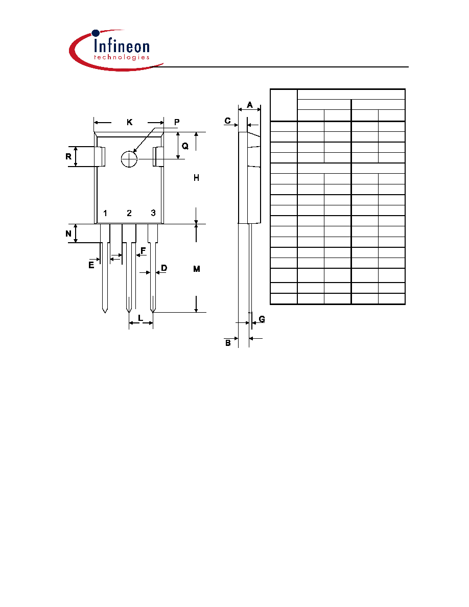
dimensions
symbol
[mm] [inch]
min max min max
A 9.70
10.30
0.3819
0.4055
B 14.88
15.95
0.5858
0.6280
C 0.65
0.86
0.0256
0.0339
D 3.55
3.89
0.1398
0.1531
E 2.60
3.00
0.1024
0.1181
F 6.00
6.80
0.2362
0.2677
G 13.00
14.00
0.5118
0.5512
H 4.35
4.75
0.1713
0.1870
K 0.38
0.65
0.0150
0.0256
L 0.95
1.32
0.0374
0.0520
M
2.54 typ.
0.1 typ.
N 4.30
4.50
0.1693
0.1772
P 1.17
1.40
0.0461
0.0551
T 2.30
2.72
0.0906
0.1071
TO-220AB
dimensions
symbol
[mm] [inch]
min max min max
A 9.80
10.20
0.3858
0.4016
B 0.70
1.30
0.0276
0.0512
C 1.00
1.60
0.0394
0.0630
D 1.03
1.07
0.0406
0.0421
E
2.54 typ.
0.1 typ.
F 0.65
0.85
0.0256
0.0335
G
5.08 typ.
0.2 typ.
H 4.30
4.50
0.1693
0.1772
K 1.17
1.37
0.0461
0.0539
L 9.05
9.45
0.3563
0.3720
M 2.30
2.50
0.0906
0.0984
N
15 typ.
0.5906 typ.
P 0.00
0.20
0.0000
0.0079
Q 4.20
5.20
0.1654
0.2047
R
8∞ max
8∞ max
S 2.40
3.00
0.0945
0.1181
T 0.40
0.60
0.0157
0.0236
U 10.80
0.4252
V 1.15
0.0453
W 6.23
0.2453
X 4.60
0.1811
Y 9.40
0.3701
TO-263AB (D
2
Pak)
Z 16.15 0.6358
IGP03N120H2, IGB03N120H2
IGW03N120H2
Power Semiconductors
11
Rev. 2, Mar-04
dimensions
symbol
[mm]
symbol
min min
A 4.78 A 4.78 A
B 2.29 B 2.29 B
C 1.78 C 1.78 C
D 1.09 D 1.09 D
E 1.73
E
F 2.67 F 2.67 F
G 0.76
max
G 0.76
max G
H 20.80 H 20.80 H
K 15.65 K 15.65 K
L 5.21 L 5.21 L
M 19.81 M 19.81 M
N 3.560 N 3.560 N
P
3.61
P
3.61
P
Q 6.12 Q 6.12 Q
dimensi
ons
dimensi
ons
symbol
[mm]
symbol
[mm]
symbol
min min
TO-247AC

IGP03N120H2, IGB03N120H2
IGW03N120H2
Power Semiconductors
12
Rev. 2, Mar-04
Figure A. Definition of switching times
I
r r m
90%
I
r r m
10%
I
r r m
di /dt
F
t
r r
I
F
i,v
t
Q
S
Q
F
t
S
t
F
V
R
di /dt
r r
Q =Q
Q
r r
S
F
+
t =t
t
r r
S
F
+
Figure C. Definition of diodes
switching characteristics
p(t)
1
2
n
T (t)
j
1
1
2
2
n
n
T
C
r
r
r
r
r
r
Figure D. Thermal equivalent
circuit
Figure E. Dynamic test circuit
Leakage inductance L
= 180nH,
Stray capacitor C
= 40pF,
Relief capacitor C
r
= 4nF (only for
ZVT switching)
Figure B. Definition of switching losses
ˆˆ
V
DC
DUT
(Diode)
Ω
L
R
G
DUT
(IGBT)
L
Ω
L
C
C
r

IGP03N120H2, IGB03N120H2
IGW03N120H2
Power Semiconductors
13
Rev. 2, Mar-04
Published by
Infineon Technologies AG i Gr.,
Bereich Kommunikation
St.-Martin-Strasse 53,
D-81541 M¸nchen
© Infineon Technologies AG 1999
All Rights Reserved.
Attention please!
The information herein is given to describe certain components and shall not be considered as warranted characteristics.
Terms of delivery and rights to technical change reserved.
We hereby disclaim any and all warranties, including but not limited to warranties of non-infringement, regarding circuits,
descriptions and charts stated herein.
Infineon Technologies is an approved CECC manufacturer.
Information
For further information on technology, delivery terms and conditions and prices please contact your nearest Infineon
Technologies Office in Germany or our Infineon Technologies Representatives worldwide (see address list).
Warnings
Due to technical requirements components may contain dangerous substances. For information on the types in question
please contact your nearest Infineon Technologies Office.
Infineon Technologies Components may only be used in life-support devices or systems with the express written
approval of Infineon Technologies, if a failure of such components can reasonably be expected to cause the failure of
that life-support device or system, or to affect the safety or effectiveness of that device or system. Life support devices or
systems are intended to be implanted in the human body, or to support and/or maintain and sustain and/or protect
human life. If they fail, it is reasonable to assume that the health of the user or other persons may be endangered.