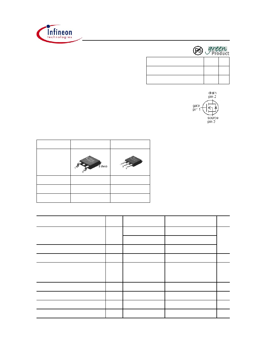
IPDH4N03LA G IPSH4N03LA G
Opti
MOS
Æ
2 Power-Transistor
Features
∑ Ideal for high-frequency dc/dc converters
∑ Qualified according to JEDEC
1)
for target applications
∑ N-channel, logic level
∑ Excellent gate charge x R
DS(on)
product (FOM)
∑ Superior thermal resistance
∑ 175 ∞C operating temperature
∑ Pb-free lead plating; RoHS compliant
Maximum ratings, at T
j
=25 ∞C, unless otherwise specified
Parameter
Symbol Conditions
Unit
Continuous drain current
I
D
T
C
=25 ∞C
2)
90
A
T
C
=100 ∞C
77
Pulsed drain current
I
D,pulse
T
C
=25 ∞C
3)
360
Avalanche energy, single pulse
E
AS
I
D
=90 A, R
GS
=25
150
mJ
Reverse diode dv /dt
dv /dt
I
D
=90 A, V
DS
=20 V,
di /dt =200 A/µs,
T
j,max
=175 ∞C
6
kV/µs
Gate source voltage
4)
V
GS
±20
V
Power dissipation
P
tot
T
C
=25 ∞C
94
W
Operating and storage temperature
T
j
, T
stg
-55 ... 175
∞C
IEC climatic category; DIN IEC 68-1
55/175/56
Value
V
DS
25
V
R
DS(on),max
(SMD Version)
4.2
m
I
D
90
A
Product Summary
Type
IPDH4N03LA G
IPSH4N03LA G
Package
P-TO252-3-11
P-TO251-3-11
Ordering Code
Q67042-S4250
Q67042-S4254
Marking
H4N03LA
H4N03LA
Rev. 0.92 - target data sheet
page 1
2004-10-27

IPDH4N03LA G IPSH4N03LA G
Parameter
Symbol Conditions
Unit
min.
typ.
max.
Thermal characteristics
Thermal resistance, junction - case
R
thJC
-
-
1.6
K/W
SMD version, device on PCB
R
thJA
minimal footprint
-
-
75
6 cm
2
cooling area
5)
-
-
50
Electrical characteristics, at T
j
=25 ∞C, unless otherwise specified
Static characteristics
Drain-source breakdown voltage
V
(BR)DSS
V
GS
=0 V, I
D
=1 mA
25
-
-
V
Gate threshold voltage
V
GS(th)
V
DS
=V
GS
, I
D
=40 µA
1.2
1.6
2
Zero gate voltage drain current
I
DSS
V
DS
=25 V, V
GS
=0 V,
T
j
=25 ∞C
-
0.1
1
µA
V
DS
=25 V, V
GS
=0 V,
T
j
=125 ∞C
-
10
100
Gate-source leakage current
I
GSS
V
GS
=20 V, V
DS
=0 V
-
10
100
nA
Drain-source on-state resistance
R
DS(on)
V
GS
=4.5 V, I
D
=50 A
-
6.1
7.6
m
V
GS
=4.5 V, I
D
=50 A,
SMD version
-
5.9
7.4
V
GS
=10 V, I
D
=60 A
-
3.7
4.4
V
GS
=10 V, I
D
=60 A,
SMD version
-
3.5
4.2
Gate resistance
R
G
-
1.3
-
Transconductance
g
fs
|V
DS
|>2|I
D
|R
DS(on)max
,
I
D
=60 A
45
90
-
S
5)
Device on 40 mm x 40 mm x 1.5 mm epoxy PCB FR4 with 6 cm
2
(one layer, 70 µm thick) copper area for drain
connection. PCB is vertical in still air.
Values
1)
Current is limited by bondwire; with an R
thJC
=1.6 K/W the chip is able to carry 109 A.
3)
See figure 3
4)
T
j,max
=150 ∞C and duty cycle D <0.25 for V
GS
<-5 V
1)
J-STD20 and JESD22
Rev. 0.92 - target data sheet
page 2
2004-10-27

IPDH4N03LA G IPSH4N03LA G
Parameter
Symbol Conditions
Unit
min.
typ.
max.
Dynamic characteristics
Input capacitance
C
iss
-
2400
3200
pF
Output capacitance
C
oss
-
920
1200
Reverse transfer capacitance
C
rss
-
110
160
Turn-on delay time
t
d(on)
-
9
14
ns
Rise time
t
r
-
7
11
Turn-off delay time
t
d(off)
-
29
44
Fall time
t
f
-
4.6
7
Gate Charge Characteristics
6)
Gate to source charge
Q
gs
-
8
11
nC
Gate charge at threshold
Q
g(th)
-
3.9
5.1
Gate to drain charge
Q
gd
-
5.6
8
Switching charge
Q
sw
-
10
14
Gate charge total
Q
g
-
19
26
Gate plateau voltage
V
plateau
-
3.4
-
V
Gate charge total, sync. FET
Q
g(sync)
V
DS
=0.1 V,
V
GS
=0 to 5 V
-
17
23
nC
Output charge
Q
oss
V
DD
=15 V, V
GS
=0 V
-
20
27
Reverse Diode
Diode continous forward current
I
S
-
-
78
A
Diode pulse current
I
S,pulse
-
-
360
Diode forward voltage
V
SD
V
GS
=0 V, I
F
=78 A,
T
j
=25 ∞C
-
0.93
1.2
V
Reverse recovery charge
Q
rr
V
R
=15 V, I
F
=I
S
,
di
F
/dt =400 A/µs
-
-
15
nC
6)
See figure 16 for gate charge parameter definition
T
C
=25 ∞C
Values
V
GS
=0 V, V
DS
=15 V,
f =1 MHz
V
DD
=15 V, V
GS
=10 V,
I
D
=25 A, R
G
=2.7
V
DD
=15 V, I
D
=45 A,
V
GS
=0 to 5 V
Rev. 0.92 - target data sheet
page 3
2004-10-27

Rev. 0.92 - target data sheet
page 4
2004-10-27

IPDH4N03LA G IPSH4N03LA G
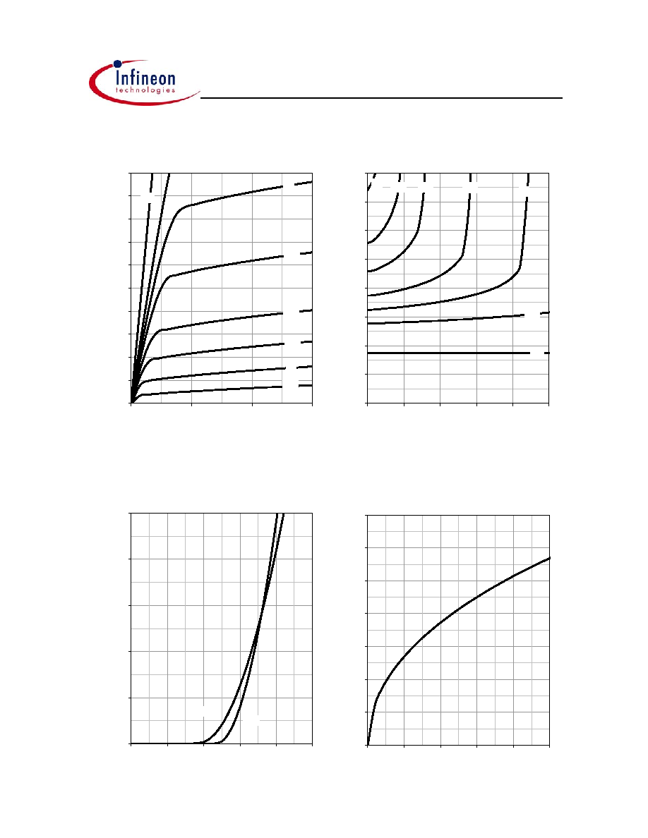
1 Power dissipation
2 Drain current
P
tot
=f(T
C
)
I
D
=f(T
C
); V
GS
10 V
3 Safe operating area
4 Max. transient thermal impedance
I
D
=f(V
DS
); T
C
=25 ∞C; D =0
Z
thJC
=f(t
p
)
parameter: t
p
parameter: D =t
p
/T
1 µs
10 µs
100 µs
1 ms
10 ms
DC
1
10
100
1000
0.1
1
10
100
V
DS
[V]
I
D
[A]
limited by on-state
resistance
single pulse
0.01
0.02
0.05
0.1
0.2
0.5
10
0
10
-1
10
-2
10
-3
10
-4
10
-5
10
-6
0.01
0.1
1
10
t
p
[s]
Z
thJ
C
[K/W]
0
20
40
60
80
100
120
0
50
100
150
200
T
C
[∞C]
P
tot
[W]
0
20
40
60
80
100
0
50
100
150
200
T
C
[∞C]
I
D
[A]
Rev. 0.92 - target data sheet
page 5
2004-10-27
IPDH4N03LA G IPSH4N03LA G
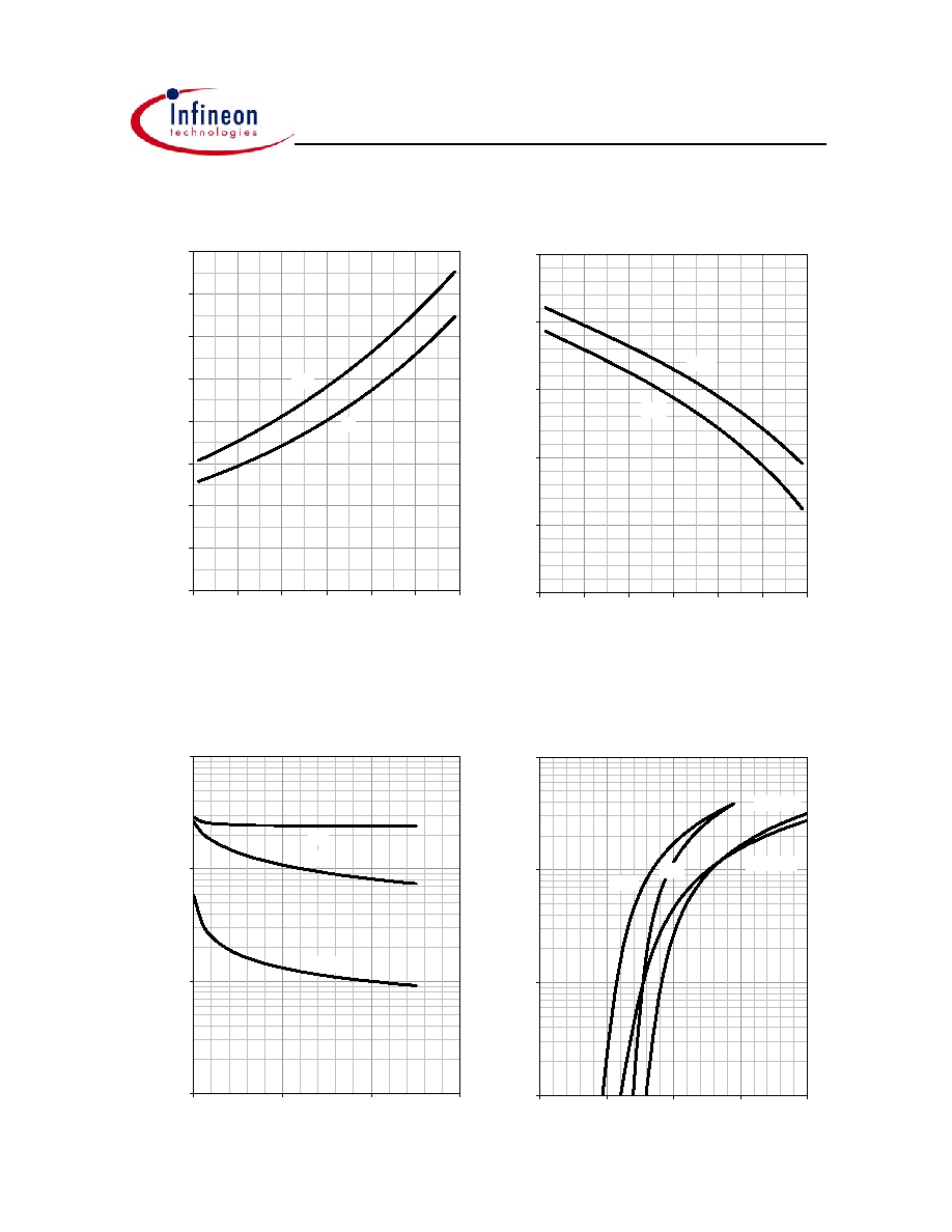
5 Typ. output characteristics
6 Typ. drain-source on resistance
I
D
=f(V
DS
); T
j
=25 ∞C
R
DS(on)
=f(I
D
); T
j
=25 ∞C
parameter: V
GS
parameter: V
GS
7 Typ. transfer characteristics
8 Typ. forward transconductance
I
D
=f(V
GS
); |V
DS
|>2|I
D
|R
DS(on)max
g
fs
=f(I
D
); T
j
=25 ∞C
parameter: T
j
3 V
3.2 V
3.4 V
3.7 V
4 V
4.5 V
10 V
0
2
4
6
8
10
12
14
16
0
20
40
60
80
100
I
D
[A]
R
DS
(on)
[m
]
25 ∞C
175 ∞C
0
20
40
60
80
100
0
1
2
3
4
5
V
GS
[V]
I
D
[A]
0
20
40
60
80
100
120
140
0
20
40
60
80
100
I
D
[A]
g
fs
[S]
2.8 V
3 V
3.2 V
3.4 V
3.7 V
4 V
4.5 V
10 V
0
10
20
30
40
50
60
70
80
90
100
0
1
2
3
V
DS
[V]
I
D
[A]
Rev. 0.92 - target data sheet
page 6
2004-10-27
IPDH4N03LA G IPSH4N03LA G
9 Drain-source on-state resistance
10 Typ. gate threshold voltage
R
DS(on)
=f(T
j
); I
D
=60 A; V
GS
=10 V
V
GS(th)
=f(T
j
); V
GS
=V
DS
parameter: I
D
11 Typ. capacitances
12 Forward characteristics of reverse diode
C =f(V
DS
); V
GS
=0 V; f =1 MHz
I
F
=f(V
SD
)
parameter: T
j
typ
98 %
0
1
2
3
4
5
6
7
8
-60
-20
20
60
100
140
180
T
j
[∞C]
R
DS
(on)
[m
]
40 µA
400 µA
0
0.5
1
1.5
2
2.5
-60
-20
20
60
100
140
180
T
j
[∞C]
V
G
S
(th)
[V]
Ciss
Coss
Crss
10
4
10
3
10
2
10
1
0
10
20
30
V
DS
[V]
C
[pF]
25 ∞C
175 ∞C
25 ∞C, 98%
175 ∞C, 98%
1
10
100
1000
0.0
0.5
1.0
1.5
2.0
V
SD
[V]
I
F
[A]
Rev. 0.92 - target data sheet
page 7
2004-10-27

IPDH4N03LA G IPSH4N03LA G
13 Avalanche characteristics
14 Typ. gate charge
I
AS
=f(t
AV
); R
GS
=25
V
GS
=f(Q
gate
); I
D
=45 A pulsed
parameter: T
j(start)
parameter: V
DD
15 Drain-source breakdown voltage
16 Gate charge waveforms
V
BR(DSS)
=f(T
j
); I
D
=1 mA
5 V
15 V
20 V
0
2
4
6
8
10
12
0
10
20
30
40
Q
gate
[nC]
V
GS
[V]
20
21
22
23
24
25
26
27
28
29
-60
-20
20
60
100
140
180
T
j
[∞C]
V
BR(DS
S
)
[V]
V
GS
Q
gate
V
g s(th)
Q
g(th)
Q
g s
Q
g d
Q
sw
Q
g
25 ∞C
100 ∞C
150 ∞C
1
10
100
1
10
100
1000
t
AV
[µs]
I
AV
[A]
Rev. 0.92 - target data sheet
page 8
2004-10-27
IPDH4N03LA G IPSH4N03LA G
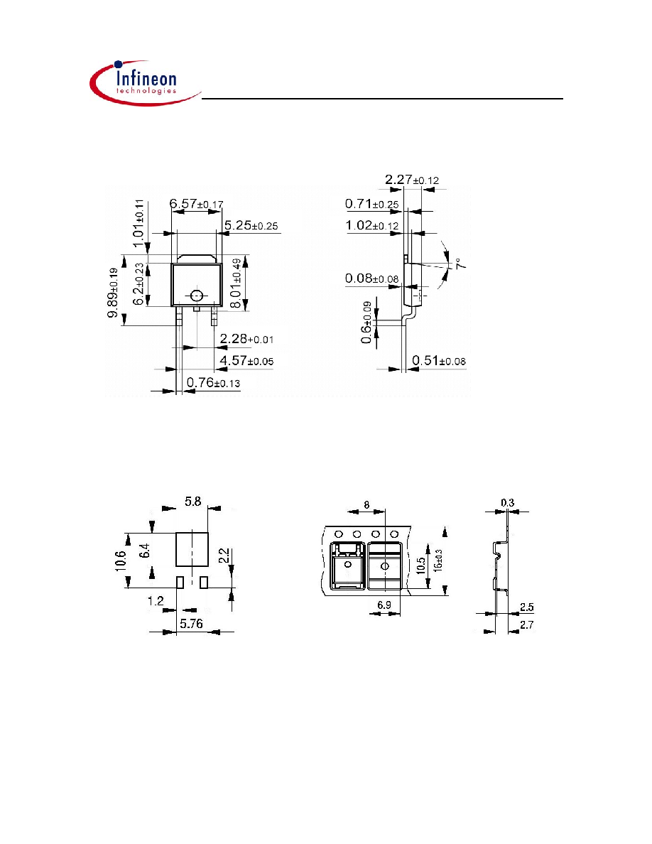
Package Outline
P-TO252-3-11: Outline
Footprint:
Packaging:
Dimensions in mm
Rev. 0.92 - target data sheet
page 9
2004-10-27