2001-07-05
Page 1
SPP11N60C3, SPB11N60C3
SPI11N60C3
Preliminary data
Cool MOSTM
=
=
=
=
Power Transistor
C
Power Semiconductors
O
O L
MOS
Feature
∑
=
New revolutionary high voltage technology
∑
Worldwide best R
DS(on)
in TO 220
∑
Ultra low gate charge
∑
=
Periodic avalanche rated
∑
Extreme dv/dt rated
∑
=
High peak current capability
∑
=
Improved transconductance
∑
=
150 ∞C operating temperature
Product Summary
V
DS
@ T
jmax
650
V
R
DS(on)
0.38
I
D
11
A
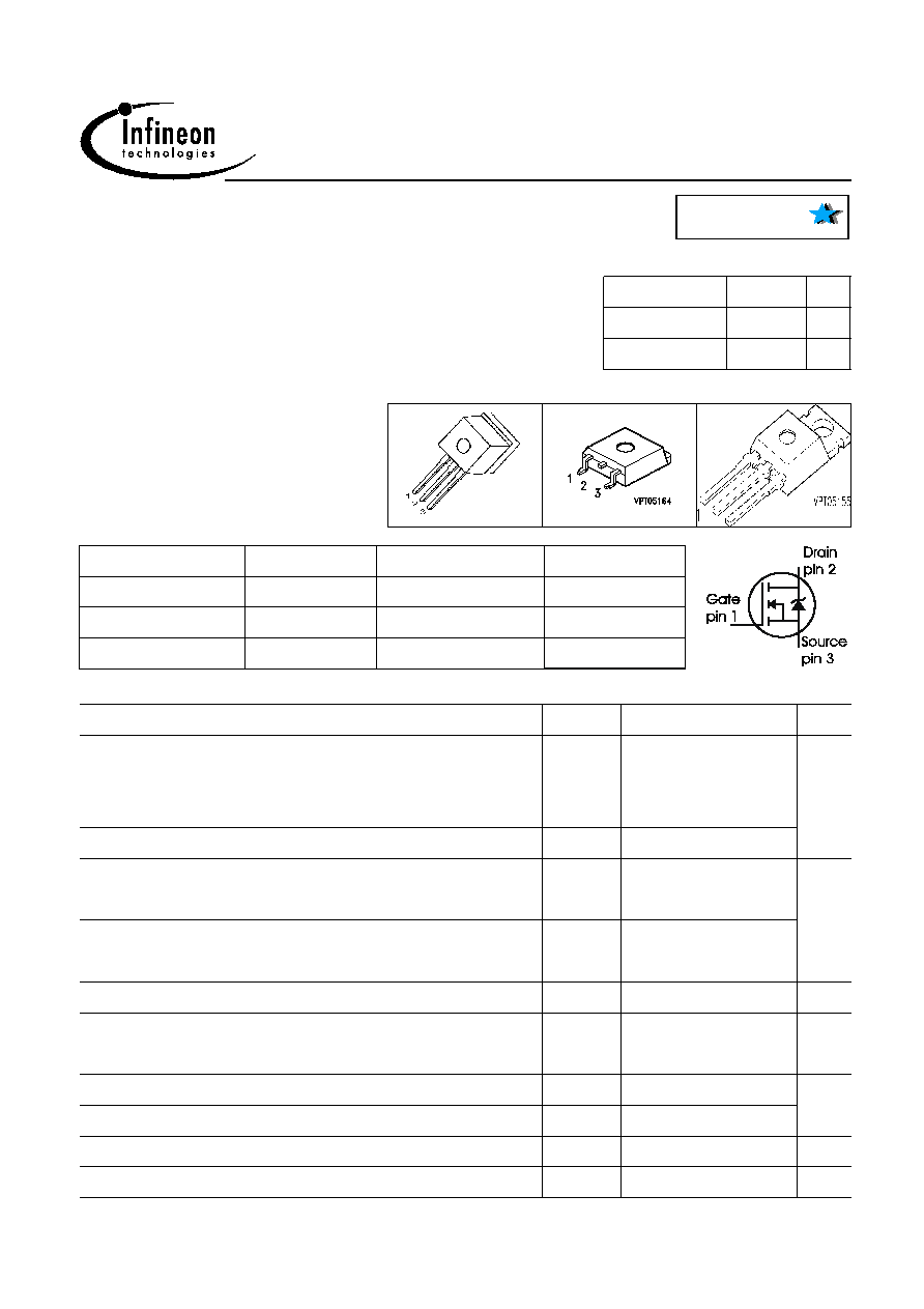
P-TO262-3-1
P-TO220-3-1
P-TO263-3-2
Type
Package
Ordering Code
SPP11N60C3
P-TO220-3-1
Q67040-S4395
SPB11N60C3
P-TO263-3-2
Q67040-S4396
SPI11N60C3
P-TO262-3-1
Q67042-S4403
Marking
11N60C3
11N60C3
11N60C3
Maximum Ratings, at T
j
= 25 ∞C, unless otherwise specified
Parameter
Symbol
Value
Unit
Continuous drain current
T
C
= 25 ∞C
T
C
= 100 ∞C
I
D
11
7
A
Pulsed drain current, t
p
limited by T
jmax
I
D puls
33
Avalanche energy, single pulse
I
D
=5.5A, V
DD
=50V
E
AS
340
mJ
Avalanche energy, repetitive t
AR
limited by T
jmax
1)
I
D
=11A, V
DD
=50V
E
AR
0.6
Avalanche current, repetitive t
AR
limited by T
jmax
I
AR
11
A
Reverse diode dv/dt
I
S
=11A, V
DS
<
=
V
DD
, di/dt=100A/µs, T
jmax
=150∞C
dv/dt
6
V/ns
Gate source voltage static
V
GS
±20
V
Gate source voltage dynamic
V
GS
±
30
Power dissipation,
T
C
= 25∞C
P
tot
125
W
Operating and storage temperature
T
j ,
T
stg
-55... +150
∞C

2001-07-05
Page 2
SPP11N60C3, SPB11N60C3
SPI11N60C3
Preliminary data
Thermal Characteristics
Parameter
Symbol
Values
Unit
min.
typ.
max.
Characteristics
Thermal resistance, junction - case
R
thJC
-
-
1
K/W
Thermal resistance, junction - ambient, leaded
R
thJA
-
-
62
SMD version, device on PCB:
@ min. footprint
@ 6 cm
2
cooling area
2)
R
thJA
-
-
-
35
62
-
Linear derating factor
-
-
1
W/K
Soldering temperature,
1.6 mm (0.063 in.) from case for 10s
T
sold
-
-
260
∞C
Electrical Characteristics, at T
j
= 25 ∞C, unless otherwise specified
Static Characteristics
Drain-source breakdown voltage
V
GS
=0V, I
D
=0.25mA
V
(BR)DSS
600
-
-
V
Drain-source avalanche breakdown voltage
V
GS
=0V, I
D
=11A
V
(BR)DS
-
700
-
Gate threshold voltage, V
GS
= V
DS
I
D
= 0.5 mA
V
GS(th)
2.1
3
3.9
Zero gate voltage drain current
V
DS
= 600 V, V
GS
= 0 V, T
j
= 25 ∞C
V
DS
= 600 V, V
GS
= 0 V, T
j
= 150 ∞C
I
DSS
-
-
-
-
25
250
µA
Gate-source leakage current
V
GS
=20V, V
DS
=0V
I
GSS
-
-
100
nA
Drain-source on-state resistance
V
GS
=10V, I
D
=7A, T
j
=25∞C
V
GS
=10V, I
D
=7A, T
j
=150∞C
R
DS(on)
-
-
0.34
1.1
0.38
1.22
Gate input resistance
f = 1 MHz, open drain
R
G
-
0.86
-
1Repetitve avalanche causes additional power losses that can be calculated as P
AV
=E
AR
*f.
2Device on 40mm*40mm*1.5mm epoxy PCB FR4 with 6cm≤ (one layer, 70 µm thick) copper area for drain
connection. PCB is vertical without blown air.

2001-07-05
Page 3
SPP11N60C3, SPB11N60C3
SPI11N60C3
Preliminary data
Electrical Characteristics , at T
j
= 25 ∞C, unless otherwise specified
Parameter
Symbol
Conditions
Values
Unit
min.
typ.
max.
Characteristics
Transconductance
g
fs
V
DS
2*I
D
*R
DS(on)max
,
I
D
=7A
-
8.3
-
S
Input capacitance
C
iss
V
GS
=0V, V
DS
=25V,
f=1MHz
-
1460
-
pF
Output capacitance
C
oss
-
610
-
Reverse transfer capacitance
C
rss
-
21
-
Effective output capacitance,
1)
energy related
C
o(er)
V
GS
=0V,
V
DS
=0V to 480V
-
45
-
pF
Effective output capacitance,
2)
time related
C
o(tr)
-
85
-
Turn-on delay time
t
d(on)
V
DD
=380V, V
GS
=0/10V,
I
D
=11A, R
G
=6.8
-
10
-
ns
Rise time
t
r
-
5
-
Turn-off delay time
t
d(off)
-
44
70
Fall time
t
f
-
5
9
Gate Charge Characteristics
Gate to source charge
Q
gs
V
DD
=480V, I
D
=11A
-
5.5
-
nC
Gate to drain charge
Q
gd
-
22
-
Gate charge total
Q
g
V
DD
=480V, I
D
=11A,
V
GS
=0 to 10V
-
45
60
Gate plateau voltage
V
(plateau)
V
DD
=480V, I
D
=11A
-
5.5
-
V
1C
o(er)
is a fixed capacitance that gives the same stored energy as C
oss
while V
DS
is rising from 0 to 80% V
DSS
.
2C
o(tr)
is a fixed capacitance that gives the same charging time as C
oss
while V
DS
is rising from 0 to 80% V
DSS
.
2001-07-05
Page 4
SPP11N60C3, SPB11N60C3
SPI11N60C3
Preliminary data
Electrical Characteristics, at T
j
= 25 ∞C, unless otherwise specified
Parameter
Symbol
Conditions
Values
Unit
min.
typ.
max.
Characteristics
Inverse diode continuous
forward current
I
S
T
C
=25∞C
-
-
11
A
Inverse diode direct current,
pulsed
I
SM
-
-
33
Inverse diode forward voltage
V
SD
V
GS
=0V, I
F
=I
S
-
1
1.2
V
Reverse recovery time
t
rr
V
R
=480V, I
F
=I
S
,
di
F
/dt=100A/µs
-
400
600
ns
Reverse recovery charge
Q
rr
-
6
-
µC
Peak reverse recovery current
I
rrm
-
41
-
A
Peak rate of fall of reverse
recovery current
di
rr
/dt
-
1200
-
A/µs
Transient Thermal Characteristics
Symbol
Value
Unit
Symbol
Value
Unit
typ.
typ.
Thermal resistance
R
th1
0.015
K/W
R
th2
0.034
R
th3
0.056
R
th4
0.124
R
th5
0.143
R
th6
0.057
Thermal capacitance
C
th1
0.0002121
Ws/K
C
th2
0.0007091
C
th3
0.001184
C
th4
0.00254
C
th5
0.011
C
th6
0.092
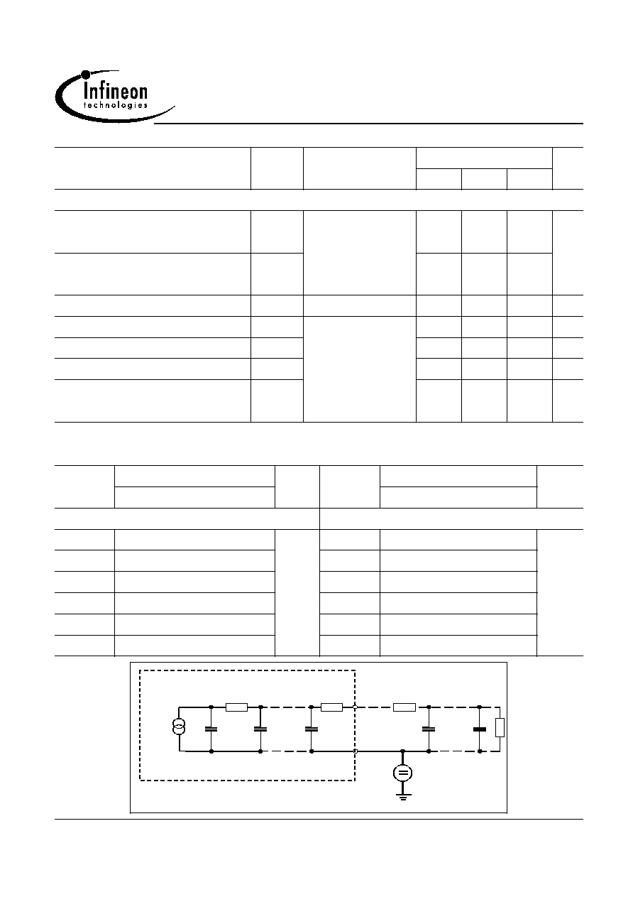
External Heatsink
T
j
T
case
T
am b
C
th1
C
th2
R
th1
R
th,n
C
th,n
P
tot
(t)
2001-07-05
Page 5
SPP11N60C3, SPB11N60C3
SPI11N60C3
Preliminary data
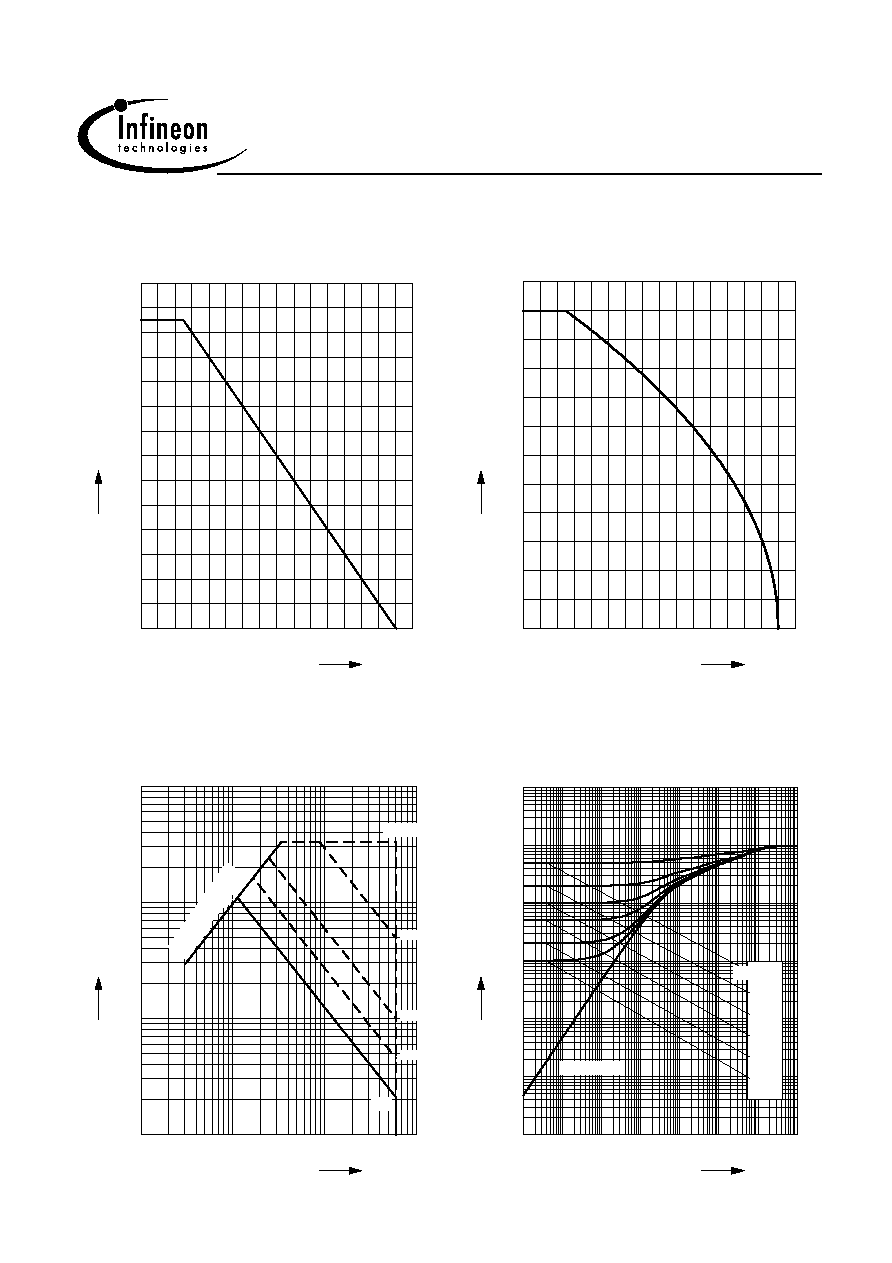
1 Power dissipation
P
tot
= f (T
C
)
0
20
40
60
80
100
120
∞C
160
T
C
0
10
20
30
40
50
60
70
80
90
100
110
120
W
140
SPP11N60C3
P
tot
2 Drain current
I
D
= f (T
C
)
parameter: V
GS
10 V
0
20
40
60
80
100
120
∞C
160
T
C
0
1
2
3
4
5
6
7
8
9
10
A
12
SPP11N60C3
I
D
3 Safe operating area
I
D
= f ( V
DS
)
parameter : D = 0 , T
C
=25∞C
10
0
10
1
10
2
10
3
V
V
DS
-1
10
0
10
1
10
2
10
A
SPP11N60C3
I
D
R
D
S(
on
)
=
V
D
S
/
I
D
DC
10 ms
1 ms
100 µs
tp = 13.0µs
4 Transient thermal impedance
Z
thJC
= f (t
p
)
parameter : D = t
p
/T
10
-7
10
-6
10
-5
10
-4
10
-3
10
-2
10
0
s
t
p
-5
10
-4
10
-3
10
-2
10
-1
10
0
10
1
10
K/W
SPP11N60C3
Z
thJC
single pulse
0.01
0.02
0.05
0.10
0.20
D = 0.50