Äîêóìåíòàöèÿ è îïèñàíèÿ www.docs.chipfind.ru
2004-01-27
Page 1
BTS 4142N
Smart High-Side Power Switch
1 Channel: 1 x 200m
Features
·
Short circuit protection
·
Current limitation
·
Overload protection
·
Overvoltage protection (including load dump)
·
Undervoltage shutdown with auto-
restart and hysteresis
·
Switching inductive loads
·
Clamp of negative voltage at output
with inductive loads
·
CMOS compatible input
·
Thermal shutdown with restart
·
ESD - Protection
·
Loss of GND and loss of V
bb
protection
·
Very low standby current
·
Reverse battery protection with external resistor
·
Improved electromagnetic compatibility (EMC)
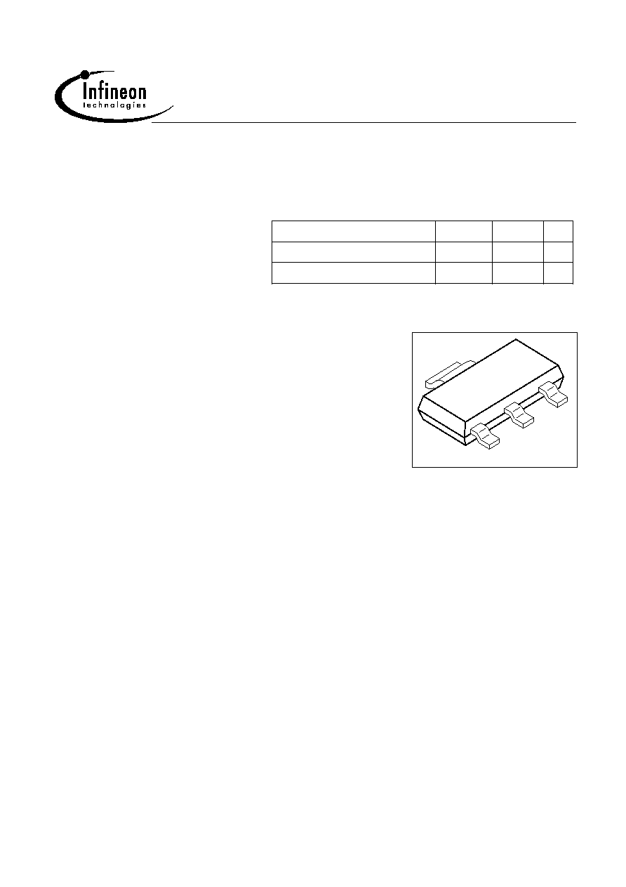
Product Summary
Overvoltage protection
V
bb(AZ)
47
V
Operating voltage
V
bb(on)
12...45 V
On-state resistance
R
ON
200
m
SOT-223
VPS05163
1
2
3
4
Application
·
All types of resistive, inductive and capacitive loads
·
µC compatible power switch for 12 V and 24 V DC applications
·
Replaces electromechanical relays and discrete circuits
General Description
N channel vertical power FET with charge pump, ground referenced CMOS compatible input,
monolithically integrated in Smart SIPMOS
technology.
Providing embedded protective functions.
2004-01-27
Page 2
BTS 4142N
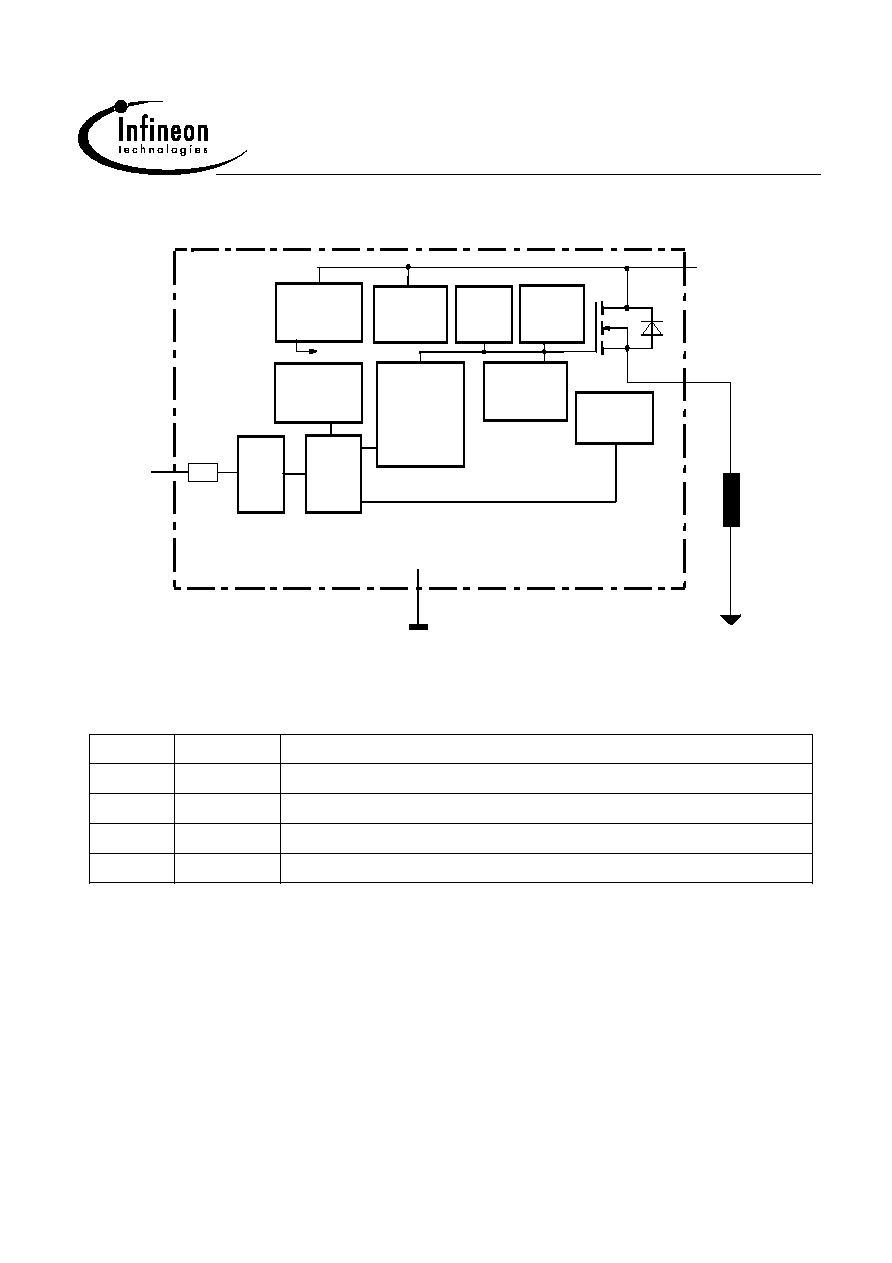
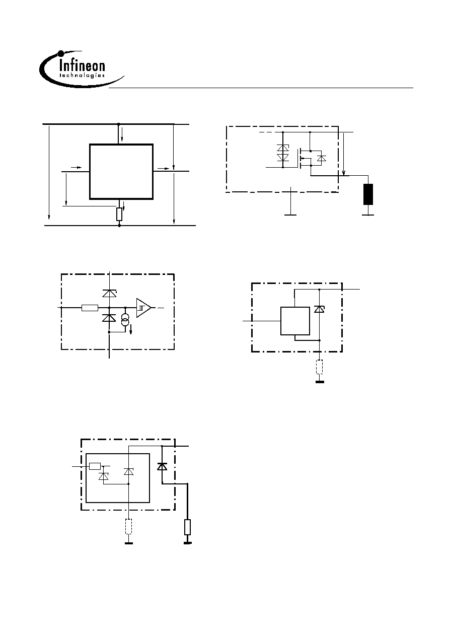
Block Diagram
IN
3
Rin
+ Vbb
Signal GND
ESD
miniPROFET
®
OUT
GND
Logic
Voltage
sensor
Voltage
source
Charge pump
Level shifter
Temperature
sensor
Rectifier
Limit for
unclamped
ind. loads
Gate
protection
Current
limit
2
4
1
Load GND
Load
V
Logic
Overvoltage
protection
Function
Output to the load
Logic ground
Input, activates the power switch in case of logic high signal
Positive power supply voltage
Pin
Symbol
1
OUT
2
GND
3
IN
4
Vbb

2004-01-27
Page 3
BTS 4142N
Maximum Ratings
Parameter
at T
j
= 25°C, unless otherwise specified
Symbol
Value
Unit
Supply voltage
V
bb
-0,3
1)
...48
V
Continuous input voltage
2)
V
IN
-10...V
bb
Load current (Short - circuit current, see page 5) I
L
self limited
A
Current through input pin (DC)
I
IN
±
5
mA
Reverse current through GND-pin
3)
-I
GND
-0.5
A
Operating temperature
T
j
internal limited
°C
Storage temperature
T
stg
-55 ... +150
Power dissipation
4)
P
tot
1.4
W
Inductive load switch-off energy dissipation
4)5)
single pulse
T
j
= 125 °C, I
L
= 1 A
E
AS
0.16
J
Load dump protection
5)
V
LoadDump
6)
= V
A
+ V
S
R
I
=2
, t
d
=400ms, V
IN
= low or high, V
A
=13,5V
R
L
= 47
V
Loaddump
83
V
Electrostatic discharge voltage
(Human Body Model)
according to ANSI EOS/ESD - S5.1 - 1993
ESD STM5.1 - 1998
Input pin
All other pins
V
ESD
±
1
±
5
kV
1defined by Ptot
2At VIN > Vbb, the input current is not allowed to exceed ±5 mA.
3defined by Ptot
4Device on 50mm*50mm*1.5mm epoxy PCB FR4 with 6 cm2 (one layer, 70µm thick) copper area for Vbb
connection. PCB is vertical without blown air.
5not subject to production test, specified by design
6VLoaddump is setup without the DUT connected to the generator per ISO 7637-1 and DIN 40839 .
Supply voltages higher than Vbb(AZ) require an external current limit for the GND pin, e.g. with a
150
resistor in GND connection. A resistor for the protection of the input is integrated.

2004-01-27
Page 4
BTS 4142N
Electrical Characteristics
Parameter
Symbol
Values
Unit
at T
j
= -40...125 °C, V
bb
= 15...30 V unless otherwise specified
min.
typ.
max.
Thermal Characteristics
Thermal resistance @ min. footprint
R
th(JA)
-
-
125
K/W
Thermal resistance @ 6 cm
2
cooling area
1)
R
th(JA)
-
-
70
Thermal resistance, junction - soldering point
R
thJS
-
-
7
K/W
Load Switching Capabilities and Characteristics
On-state resistance
T
j
= 25 °C, I
L
= 0.5 A
T
j
= 125 °C
R
ON
-
-
150
270
200
320
m
Nominal load current
2)
Device on PCB
1)
I
L(nom)
1.4
-
-
A
Turn-on time to 90%
V
OUT
R
L
= 47
, V
IN
= 0 to 10 V
t
on
-
50
100
µs
Turn-off time to 10%
V
OUT
R
L
= 47
, V
IN
= 10 to 0 V
t
off
-
75
150
Slew rate on 10 to 30% V
OUT
,
R
L
= 47
, V
bb
= 15 V
dV/dt
on
-
1
2
V/µs
Slew rate off 70 to 40% V
OUT
,
R
L
= 47
, V
bb
= 15 V
-dV/dt
off
-
1
2
1Device on 50mm*50mm*1.5mm epoxy PCB FR4 with 6 cm2 (one layer, 70µm thick) copper area for Vbb
connection. PCB is vertical without blown air.
2Nominal load current is limited by the current limitation ( see page 5 )

2004-01-27
Page 5
BTS 4142N
Electrical Characteristics
Parameter
Symbol
Values
Unit
at T
j
= -40...125 °C, V
bb
= 15...30 V unless otherwise specified
min.
typ.
max.
Operating Parameters
Operating voltage
V
bb(on)
12
-
45
V
Undervoltage shutdown
V
bb(under)
7
-
10.5
Undervoltage restart
V
bb(u rst)
-
-
11
Undervoltage hysteresis
V
bb(under)
= V
bb(u rst)
- V
bb(under)
V
bb(under)
-
0.5
-
Standby current
T
j
= -40...85 °C, V
IN
1,2 V
T
j
= 125 °C
1)
I
bb(off)
-
-
10
-
25
50
µA
Operating current
I
GND
-
1
1.6
mA
Leakage output current (included in
I
bb(off)
)
V
IN
1,2 V
I
L(off)
-
3.5
10
µA
Protection Functions
2)
Initial peak short circuit current limit
T
j
= -40 °C, V
bb
= 20 V, t
m
= 150 µs
T
j
= 25 °C
T
j
= 125 °C
I
L(SCp)
-
-
1.4
-
3
-
4.5
-
-
A
Repetitive short circuit current limit
T
j
= T
jt
(see timing diagrams)
I
L(SCr)
-
2.2
-
Output clamp (inductive load switch off)
at V
OUT
= V
bb
- V
ON(CL)
, I
bb
= 4 mA
V
ON(CL)
62
68
-
V
Overvoltage protection
3)
I
bb
= 4 mA
V
bb(AZ)
47
-
-
Thermal overload trip temperature
4)
T
jt
135
-
-
°C
Thermal hysteresis
T
jt
-
10
-
K
1higher current due temperature sensor
2Integrated protection functions are designed to prevent IC destruction under fault conditions
described in the data sheet. Fault conditions are considered as "outside" normal operating range.
Protection functions are not designed for continuous repetitive operation.
3see also VON(CL) in circuit diagram
4 higher operating temperature at normal function available

2004-01-27
Page 6
BTS 4142N
Electrical Characteristics
Parameter
Symbol
Values
Unit
at T
j
= -40...125 °C, V
bb
= 15...30 V unless otherwise specified
min.
typ.
max.
Input
Continuous input voltage
1)
V
IN
-10
2)
-
V
bb
V
Input turn-on threshold voltage
V
IN(T+)
-
-
3.0
Input turn-off threshold voltage
V
IN(T-)
1.82
-
-
Input threshold hysteresis
V
IN(T)
-
0.2
-
Off state input current
V
IN
1,8 V
I
IN(off)
20
-
-
µA
On state input current
I
IN(on)
-
-
110
Input delay time at switch on V
bb
t
d(Vbbon)
150
340
-
µs
Input resistance (see page 8)
R
I
1.5
3
5
k
Reverse Battery
Reverse battery voltage
3)2)
R
GND
= 0
R
GND
= 150
-V
bb
-
-
-
-
0.3
45
V
Continuous reverse drain current
2)
T
j
= 25 °C
I
S
-
-
1
A
Drain-source diode voltage (V
OUT
> V
bb
)
I
F
= 1 A
-V
ON
-
0.6
1.2
V
1At VIN > Vbb, the input current is not allowed to exceed ±5 mA.
2not subject to production test, guaranted by design
3defined by Ptot
2004-01-27
Page 7
BTS 4142N
EMC-Characteristics
All EMC-Characteristics are based on limited number of sampels and no part of production test.
Test Conditions:
If not other specified the test circuitry is the minimal functional configuration without any external
components for protection or filtering.
Supply voltage: Vbb = 13.5V Temperature: Ta = 23
±
5°C ;
Load: RL = 220
Operation mode: PWM Frequency: 100Hz / Duty Cycle: 50%
DC On/Off
DUT-Specific.: R
GND
Fast electrical transients
Acc. ISO 7637
Test Pulse
Test Level
Test Results
Pulse Cycle Time and
On
Off
Generator Impedance
1
-200 V
C
C
500ms ; 10
2
+200 V
C
C
500ms ; 10
3a
-200 V
C
C
100ms ; 50
3b
+ 200 V
C
C
100ms ; 50
4
1)
-7 V
C
C
0,01
5
175 V
E (70V)
E (70V)
400ms ; 2
The test pulses are applied at Vbb
Definition of functional status
Class
Content
C
All functions of the device are performed as designed after exposure to disturbance.
E
One or more function of a device does not perform as designed after exposure
and can not be returned to proper operation without repairing or replacing the
device. The value after the character shows the limit.
Test circuit:
PROFET
V
OUT
IN
bb
R
L
Pulse
Bat.
R
GND
GND
1Supply voltage Vbb = 12 V instead of 13,5 V.
2004-01-27
Page 8
BTS 4142N
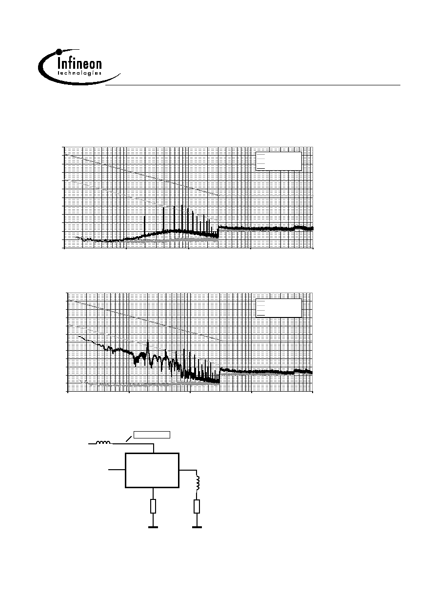
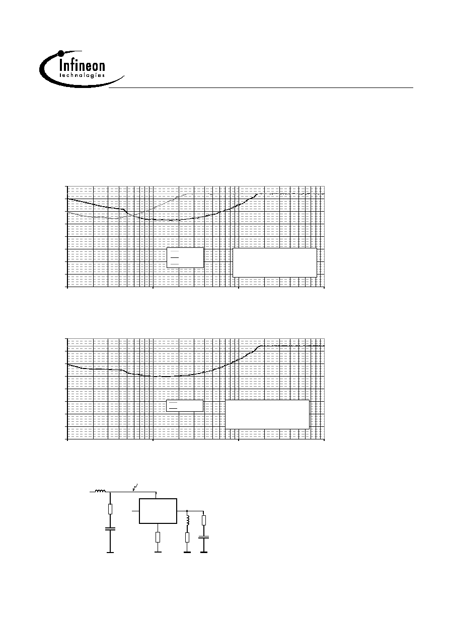
Conducted Emission
Acc. IEC 61967-4 (1
/ 150
method)
Typ. V
bb
-Pin Emission at DC-On with 150
-matching network
- 2 0
- 1 0
0
1 0
2 0
3 0
4 0
5 0
6 0
7 0
8 0
9 0
1 0 0
0 , 1
1
1 0
1 0 0
1 0 0 0
f / M H z
dBµ
V
1 5 0 o h m C la s s 6
1 5 0 o h m C la s s 1
V B B , n o is e f lo o r
V B B , O N
1 5 0
/
8 - H
1 5 0
/
1 3 - N
Typ. V
bb
-Pin Emission at PWM-Mode with 150
-matching network
- 2 0
- 1 0
0
1 0
2 0
3 0
4 0
5 0
6 0
7 0
8 0
9 0
1 0 0
0 , 1
1
1 0
1 0 0
1 0 0 0
f / M H z
dB
µ
V
1 5 0 o h m C la s s 6
1 5 0 o h m C la s s 1
V B B , n o is e f lo o r
V B B , P W M
1 5 0
/
8 - H
1 5 0
/
1 3 - N
Test circuit:
PROFET
V
OUT
IN
bb
R
5µH
5µH
150
-Network
GND
R
GND
For defined decoupling and high reproducibility a defined choke (5µH at 1 MHz)
is inserted between supply and Vbb-pin.
2004-01-27
Page 9
BTS 4142N
Conducted Susceptibility
Acc. 47A/658/CD IEC 62132-4 (Direct Power Injection)
Direct Power Injection: Forward Power CW
Failure criteria: Amplitude and frequency deviation max. 10% at Out
Typ. Vbb-Pin Susceptibility at DC-On/Off
0
5
1 0
1 5
2 0
2 5
3 0
3 5
4 0
1
1 0
1 0 0
1 0 0 0
f / M H z
dB
m
L im it
V B B , O N
V B B , O F F
D e v ic e : B T S 4 1 4 2
L o a d : 4 7 O h m s
O - M o d e : O N / O F F / P W M
C o u p lin g P o in t : V B B
M o n it o r in g : O u t
M o d u la t io n : C W
Typ. Vbb-Pin Susceptibility at PWM-Mode
0
5
1 0
1 5
2 0
2 5
3 0
3 5
4 0
1
1 0
1 0 0
1 0 0 0
f / M H z
dB
m
L im it
V B B , P W M
D e v ic e : B T S 4 1 4 2
L o a d : 4 7 O h m s
O - M o d e : O N / O F F / P W M
C o u p lin g P o in t : V B B
M o n it o r in g : O u t
M o d u la t io n : C W
Test circuit:
PROFET
V
OUT
IN
bb
R
L
HF
5µH
150
6,8nF
5µH
150
6,8nF
GND
R
GND
For defined decoupling and high reproducibility the same choke and the same
150
-matching network as for the emission measurement is used.
2004-01-27
Page 10
BTS 4142N
Terms
Inductive and overvoltage output clamp
+ V bb
OUT
GND
V Z
V
ON
PROFET
V
IN
OUT
GND
bb
VIN
IIN
V
bb
Ibb
IL
VOUT
IGND
VON
RGND
V
ON
clamped to 63 V min.
Input circuit (ESD protection)
Overvoltage protection of logic part
IN
GND
I
R
I
I
Vbb
+ Vbb
IN
GND
GND
R
Signal GND
Logic
VZ2
optional
The use of ESD zener diodes as voltage clamp
at DC conditions is not recommended
V
Z2
=V
bb(AZ)
=47V min.,
R
I
=3 k
typ., R
GND
=150
Reverse battery protection
GND
Logic
IN
OUT
L
R
Power GND
GND
R
Signal GND
Power
Inverse
I
R
Vbb
-
Diode
optional
R
GND
=150
, R
I
=3k
typ.,
Temperature protection is not active during inverse
current
2004-01-27
Page 11
BTS 4142N
GND disconnect
Inductive Load switch-off energy
dissipation
PROFET
V
IN
OUT
GND
bb
V
bb
V
IN
V
GND
PROFET
V
IN
OUT
GND
bb
=
E
E
E
EAS
bb
L
R
ELoad
RL
L
{
L
Z
GND disconnect with GND pull up
PROFET
V
IN
OUT
GND
bb
V
bb
V
GND
V
IN
Energy stored in load inductance: E
L
= ½ * L * I
L
2
While demagnetizing load inductance,
the enérgy dissipated in PROFET is
E
AS
= E
bb
+ E
L
- E
R
=
V
ON(CL)
* i
L
(t) dt,
with an approximate solution for R
L
> 0
:
E
I
L
R
V
V
I
R
V
A S
L
L
b b
O U T C L
L
L
O U T C L
=
+
+
*
*
* (
|
) * ln (
*
|
|
)
(
)|
(
)
2
1
Vbb disconnect with charged inductive
load
PROFET
V
IN
OUT
GND
bb
V
bb
high
2004-01-27
Page 12
BTS 4142N
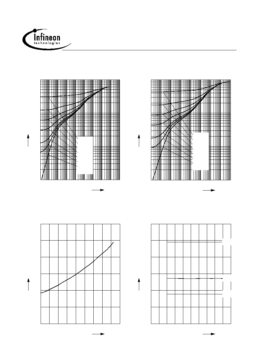
Typ. transient thermal impedance
Z
thJA
=f(t
p
) @ 6cm
2
heatsink area
Parameter: D=t
p
/T
10
-5
10
-4
10
-3
10
-2
10
-1
10
0
10
1
10
2
10
4
s
t
p
-1
10
0
10
1
10
2
10
K/W
Z
thJA
D=0,5
D=0,2
D=0,1
D=0,05
D=0,02
D=0,01
D=0
Typ. transient thermal impedance
Z
thJA
=f(t
p
) @ min. footprint
Parameter: D=t
p
/T
10
-5
10
-4
10
-3
10
-2
10
-1
10
0
10
1
10
3
s
t
p
-1
10
0
10
1
10
2
10
K/W
Z
thJA
D=0,5
D=0,2
D=0,1
D=0,05
D=0,02
D=0,01
D=0
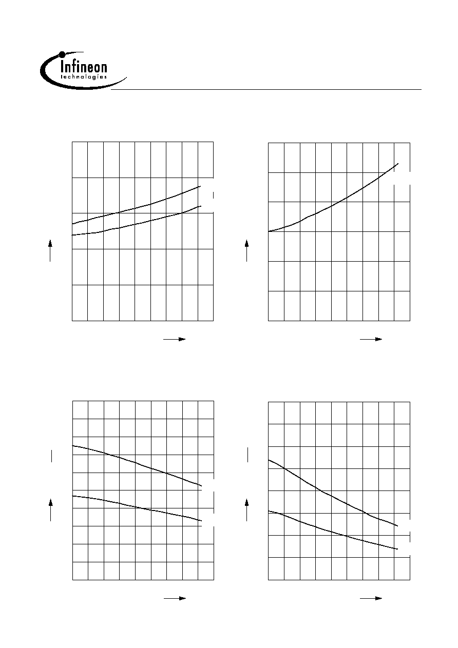
Typ. on-state resistance
R
ON
= f(T
j
) ; V
bb
= 15 V ; V
in
= high
-40
-20
0
20
40
60
80
100
°C
140
T
j
0
50
100
150
200
m
300
R
ON
Typ. on-state resistance
R
ON
= f(V
bb
); I
L
= 0.5A ; V
in
= high
0
5
10
15
20
25
30
35
40
V
50
V
bb
0
50
100
150
200
m
300
R
ON
25°C
125°C
-40°C
2004-01-27
Page 13
BTS 4142N
Typ. turn on time
t
on
= f(T
j
); R
L
= 47
-40
-20
0
20
40
60
80
100
°C
140
T
j
0
20
40
60
µs
100
t
on
15V
30V
Typ. turn off time
t
off
= f(T
j
); R
L
= 47
-40
-20
0
20
40
60
80
100
°C
140
T
j
0
20
40
60
80
µs
120
t
off
15...30V
Typ. slew rate on
dV/dt
on
= f(T
j
) ; R
L
= 47
-40
-20
0
20
40
60
80
100
°C
140
T
j
0
0.2
0.4
0.6
0.8
1
1.2
1.4
1.6
V/µs
2
d
V dt
on
30V
15V
Typ. slew rate off
dV/dt
off
= f(T
j
); R
L
= 47
-40
-20
0
20
40
60
80
100
°C
140
T
j
0
0.5
1
1.5
2
2.5
3
V/µs
4
-d
V
d
t
off
30V
15V
2004-01-27
Page 14
BTS 4142N
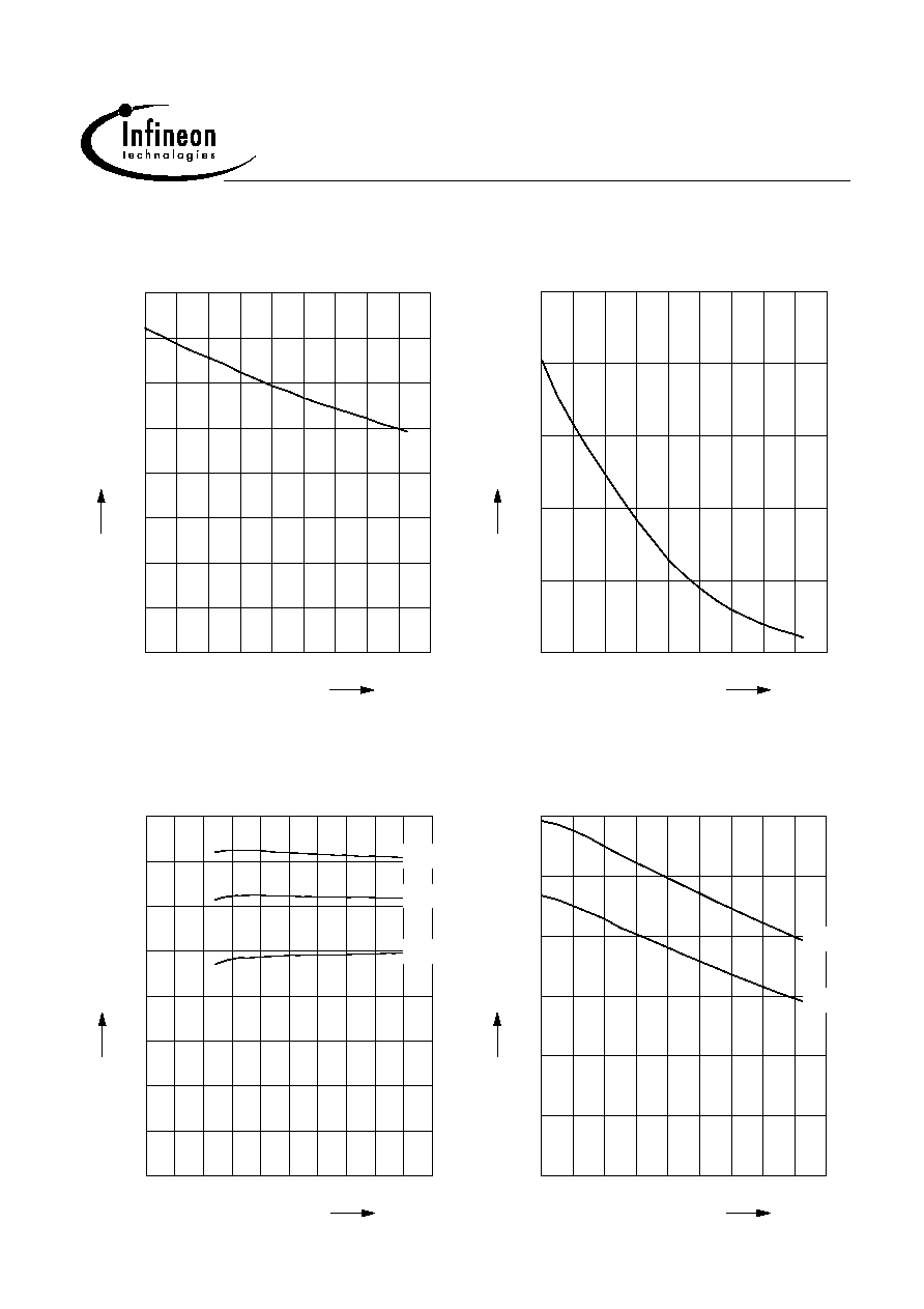
Typ. initial peak short circuit current limit
I
L(SCp)
= f(T
j
) ; V
bb
= 20V; t
m
= 150µs
-40
-20
0
20
40
60
80
100
°C
140
T
j
0
0.5
1
1.5
2
2.5
3
A
4
I
L(SCp)
Typ. initial short circuit shutdown time
t
off(SC)
= f(T
j,start
) ; V
bb
= 20V
-40
-20
0
20
40
60
80
100
°C
140
T
j
0
5
10
15
ms
25
t
off(SC)
Typ. initial peak short circuit current limit
I
L(SCp)
= f(V
bb
); t
m
= 150µs
0
5
10
15
20
25
30
35
40
V
50
V
bb
0
0.5
1
1.5
2
2.5
3
A
4
I
L(SCp)
25°C
-40°C
125°C
Typ. input current
I
IN(on/off)
= f(T
j
); V
bb
= 15 V; V
IN
= low/high
V
IN
low
1,8V;
V
IN
high
= 5V
-40
-20
0
20
40
60
80
100
°C
140
T
j
0
10
20
30
40
µA
60
I
IN
off
on
2004-01-27
Page 15
BTS 4142N
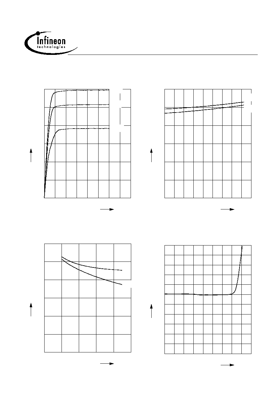
Typ. input current
I
IN
= f(V
IN
); V
bb
=15 V
0
2.5
5
7.5
10
12.5
15
V
20
V
IN
0
10
20
30
40
µA
60
I
IN
25°C
125°C
-40°C
Typ. input threshold voltage
V
IN(th)
= f(T
j
) ; V
bb
= 15 V
-40
-20
0
20
40
60
80
100
°C
140
T
j
0
0.5
1
1.5
2
V
3
V
IN(th)
on
off
Typ. input threshold voltage
V
IN(th)
= f(V
bb
) ; T
j
= 25°C
0
10
20
30
V
50
V
bb
0
0.5
1
1.5
2
V
3
V
IN(th)
on
off
Typ. standby current
I
bb(off)
= f(T
j
) ; V
bb
= 32V ; V
IN
1,2 V
-40
-20
0
20
40
60
80
100
°C
140
T
j
0
2
4
6
8
10
12
14
16
18
µA
22
I
bb(off)
2004-01-27
Page 16
BTS 4142N
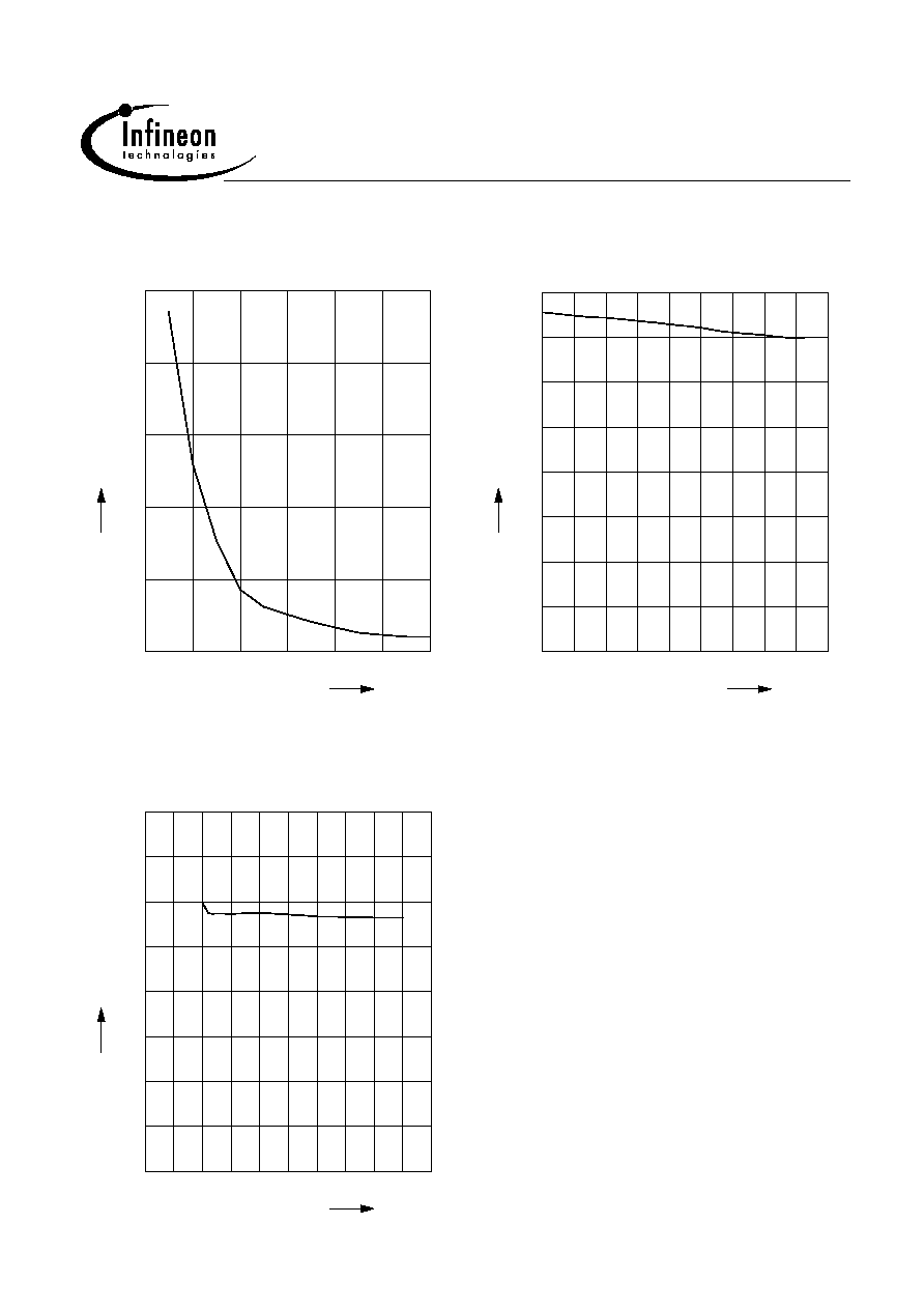
Maximum allowable inductive switch-off
energy, single pulse
E
AS
= f(I
L
); T
jstart
= 125°C
0.2
0.4
0.6
0.8
1
A
1.4
I
L
0
0.5
1
1.5
J
2.5
E
AS
Typ. leakage current
I
L(off)
= f(T
j
) ; V
bb
= 32V ; V
IN
1,2 V
-40
-20
0
20
40
60
80
100
°C
140
T
j
0
0.5
1
1.5
2
2.5
3
µA
4
I
L(off)
Typ. input delay time at switch on V
bb
t
d(Vbbon)
= f(V
bb
)
0
5
10
15
20
25
30
35
40
V
50
V
bb
0
50
100
150
200
250
300
µs
400
t
d(Vbbon)
2004-01-27
Page 17
BTS 4142N
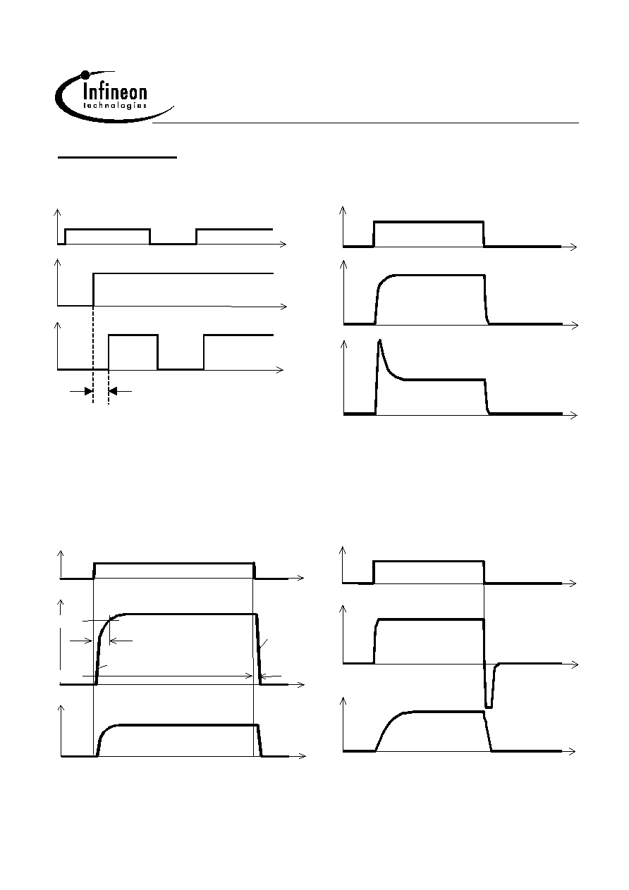
Timing diagrams
Figure 2b: Switching a lamp
Figure 1a: Vbb turn on:
IN
OUT
L
V
I
t
IN
V
L
t
I
bb
t
d(Vbbon)
Figure 2a: Switching a resistive load,
turn-on/off time and slew rate definition
Figure 2c: Switching an inductive load
IN
t
V
OUT
I
L
t
t
on
off
90%
dV/dton
dV/dtoff
10%
IN
V
I
OUT
L
t
2004-01-27
Page 18
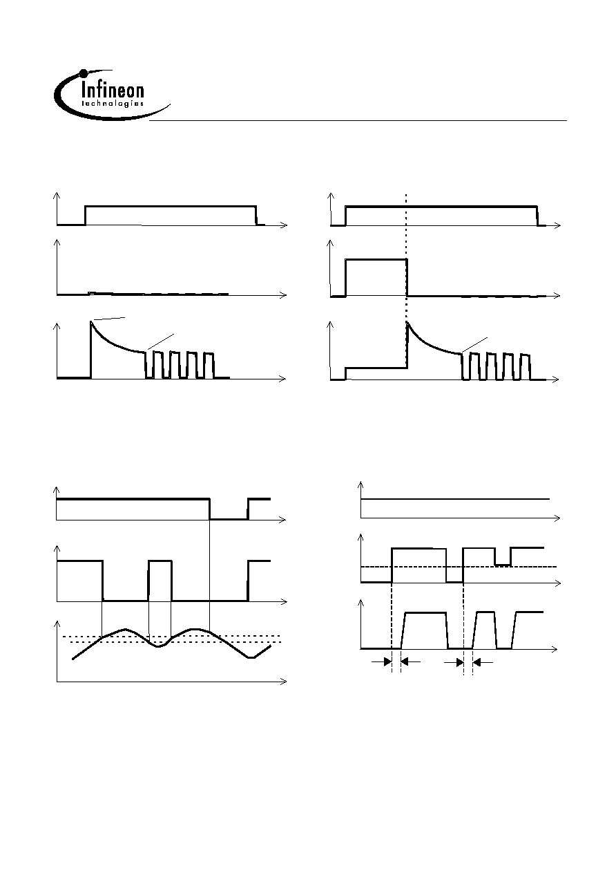
BTS 4142N
Figure 3b:
Short circuit in on-state
shut down by overtemperature, restart by cooling
Figure 3a:
Turn on into short circuit,
shut down by overtemperature, restart by cooling
IN
L
t
I
L(SCr)
I
V
OUT
Output short to GND
normal
operation
IN
L
t
I
L(SCr)
I
I
L(SCp)
V
OUT
Output short to GND
Heating up of the chip may require several milliseconds, depending
on external conditions.
Figure 5:
Undervoltage shutdown and restart
Figure 4
: Overtemperature:
Reset if Tj < Tjt
IN
OUT
J
t
V
T
IN
V
t
bb
t
d(Vbbon)
Vout
10,5V
t
d(Vbbon)
2004-01-27
Page 19
BTS 4142N
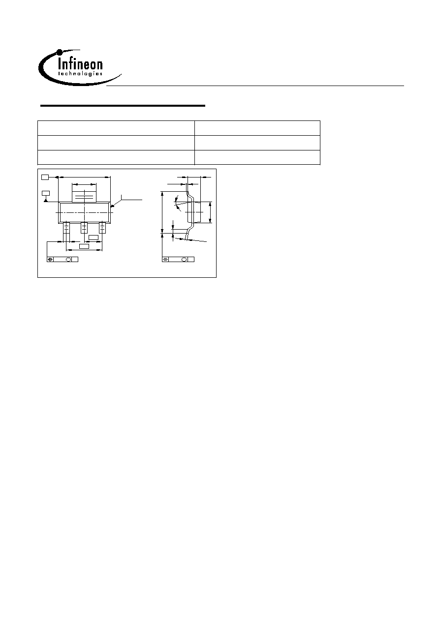
Package and ordering code
all dimensions in mm
Sales code
BTS 4142N
Ordering code, standard (1000 pcs.)
Q67060-S6121
Ordering code, optional (4000 pcs.)
Q67060-S6128
±0.1
±0.2
±0.1
0.7
4
3
2
1
GPS05560
6.5
3
acc. to
+0.2
DIN 6784
1.6
±0.1
15° max
±0.04
0.28
7
±0.3
±0.2
3.5
0.5
0.1 max
min
B
M
0.25
B
A
2.3
4.6
A
M
0.25
Published by
Infineon Technologies AG,
St.-Martin-Strasse 53,
D-81669 München
© Infineon Technologies AG 2001
All Rights Reserved.
Attention please!
The information herein is given to describe certain components and shall not be considered as a guarantee
of characteristics.
Terms of delivery and rights to technical change reserved.
We hereby disclaim any and all warranties, including but not limited to warranties of non-infringement,
regarding circuits, descriptions and charts stated herein.
Infineon Technologies is an approved CECC manufacturer.
Information
For further information on technology, delivery terms and conditions and prices please contact your
nearest Infineon Technologies Office in Germany or our Infineon Technologies Representatives worldwide
(see address list).
Warnings
Due to technical requirements components may contain dangerous substances. For information on the
types in question please contact your nearest Infineon Technologies Office.
Infineon Technologies Components may only be used in life-support devices or systems with the express
written approval of Infineon Technologies, if a failure of such components can reasonably be expected to
cause the failure of that life-support device or system, or to affect the safety or effectiveness of that device
or system. Life support devices or systems are intended to be implanted in the human body, or to support
and/or maintain and sustain and/or protect human life. If they fail, it is reasonable to assume that the health
of the user or other persons may be endangered.