
PROFETÆ BTS 432 I2
Infineon Technologies AG
Page 1 of 15
1999-02-19
Smart Highside Power Switch
Features
∑
Load dump and reverse battery protection
1)
∑
Clamp of negative voltage at output
∑
Short-circuit protection
∑
Current limitation
∑
Thermal shutdown
∑
Diagnostic feedback
∑
Open load detection in OFF-state
∑
CMOS compatible input
∑
Electrostatic discharge (ESD) protection
∑
Loss of ground and loss of V
bb
protection
2)
∑
Overvoltage protection
∑
Undervoltage and overvoltage shutdown with auto-restart and
hysteresis
Application
∑
µ
C compatible power switch with diagnostic feedback
for 12 V and 24 V DC grounded loads
∑
All types of resistive, inductive and capacitve loads
∑
Replaces electromechanical relays and discrete circuits
General Description
N channel vertical power FET with charge pump, ground referenced CMOS compatible input and diagnostic
feedback, integrated in Smart SIPMOS
Æ
chip on chip technology. Fully protected by embedded protection
functions.
+ Vbb
IN
ST
Signal GND
ESD
PROFET
Æ
OUT
GND
Logic
Voltage
sensor
Voltage
source
Open load
detection
Short circuit
detection
Charge pump
Level shifter
Temperature
sensor
Rectifier
Limit for
unclamped
ind. loads
Gate
protection
Current
limit
2
4
1
3
5
Load GND
Load
V
Logic
Overvoltage
protection
R bb
1)
No external components required, reverse load current limited by connected load.
2)
Additional external diode required for charged inductive loads
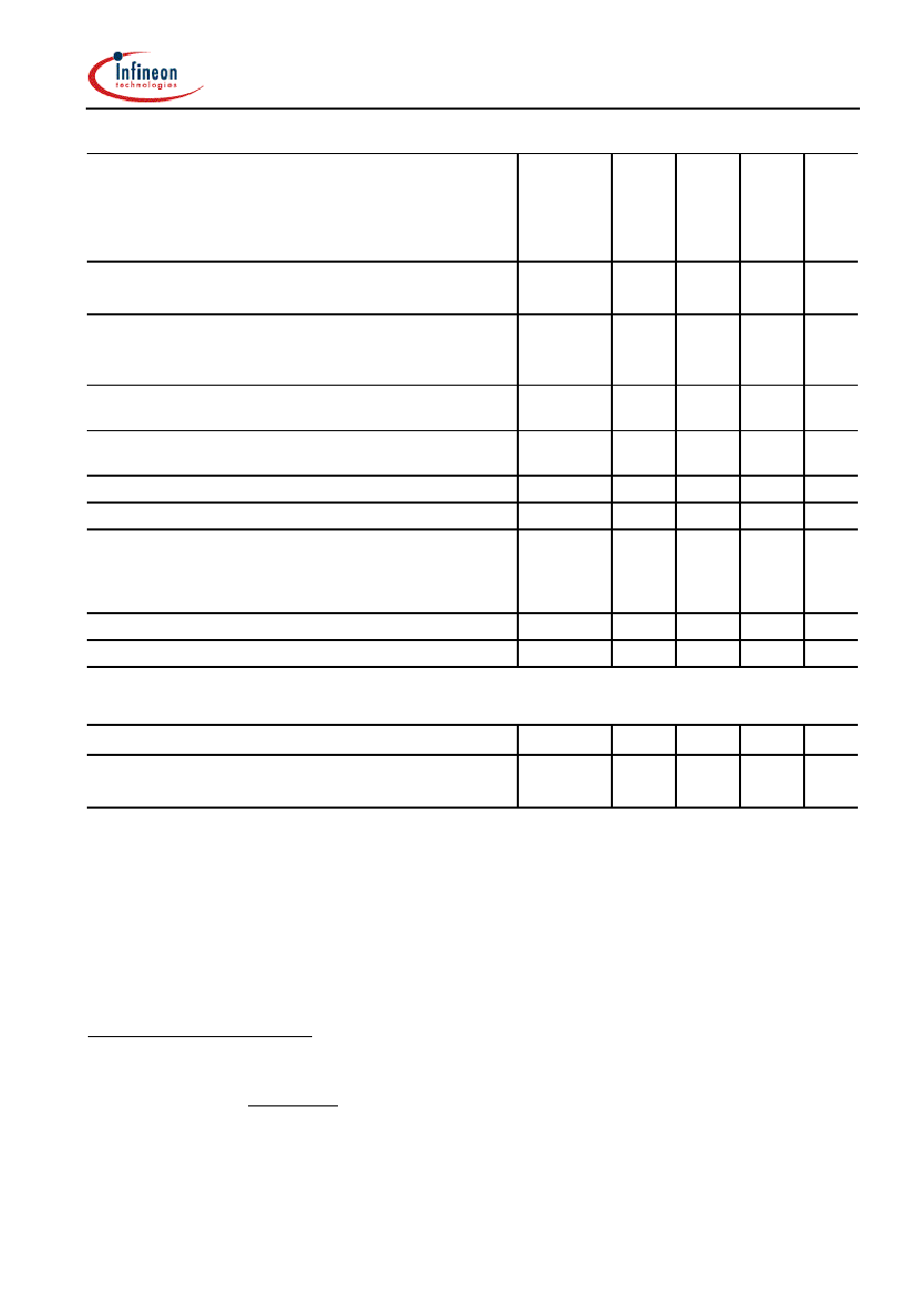
Product Summary
V
Load dump
80
V
V
bb
-V
OUT
Avalanche Clamp
58
V
V
bb (operation)
4.5 ... 42
V
V
bb (reverse)
-32
V
R
ON
38
m
I
L(SCp)
42
A
I
L(SCr)
33
A
I
L(ISO)
11
A
1
5
SMD
5
Standard

BTS 432 I2
Infineon Technologies AG
Page 2
1999-02-19
Pin
Symbol
Function
1
GND
-
Logic ground
2
IN
I
Input, activates the power switch in case of logical high signal
3
Vbb
+
Positive power supply voltage,
the tab is shorted to this pin
4
ST
S
Diagnostic feedback, low on failure
5
OUT
(Load, L)
O
Output to the load
Maximum Ratings at T
j
= 25 ∞C unless otherwise specified
Parameter
Symbol
Values
Unit
Supply voltage (overvoltage protection see page 3)
V
bb
63
V
Load dump protection V
LoadDump
= U
A
+ V
s
, U
A
= 13.5 V
R
I
= 2
, R
L
= 1.1
, t
d
= 200 ms, IN= low or high
V
s3
)
66.5
V
Load current (Short-circuit current, see page 4)
I
L
self-limited
A
Operating temperature range
Storage temperature range
T
j
T
stg
-40 ...+150
-55 ...+150
∞C
Power dissipation (DC)
P
tot
125
W
Inductive load switch-off energy dissipation,
single pulse
T
j
=150 ∞C: E
AS
1.7
J
Electrostatic discharge capability (ESD)
(Human Body Model)
V
ESD
2.0
kV
Input voltage (DC)
V
IN
-0.5 ... +6
V
Current through input pin (DC)
Current through status pin (DC)
see internal circuit diagrams page 6...
I
IN
I
ST
±
5.0
±
5.0
mA
Thermal resistance
chip - case:
junction - ambient (free air):
R
thJC
R
thJA
1
75
K/W
SMD version, device on pcb
4)
:
tbd
3)
V
S
is setup without DUT connected to the generator per ISO 7637-1 and DIN 40839
4
) Device on 50mm*50mm*1.5mm epoxy PCB FR4 with 6cm
2
(one layer, 70
µ
m thick) copper area for Vbb
connection. PCB is vertical without blown air.

BTS 432 I2
Infineon Technologies AG
Page 3
1999-02-19
Electrical Characteristics
Parameter and Conditions
Symbol
Values
Unit
at T
j
= 25 ∞C, V
bb
= 12 V unless otherwise specified
min
typ
max
Load Switching Capabilities and Characteristics
On-state resistance (pin 3 to 5)
I
L
= 2 A
T
j
=25 ∞C:
T
j
=150 ∞C:
R
ON
--
30
55
38
70
m
Nominal load current (pin 3 to 5)
ISO Proposal: V
ON
= 0.5 V, T
C
= 85 ∞C
I
L(ISO)
9
11
--
A
Output current (pin
5
) while GND disconnected or
GND pulled up, V
IN
= 0, see diagram page 7,
T
j
=-40...+150∞C
I
L(GNDhigh)
--
--
1
mA
Turn-on time
to 90% V
OUT
:
Turn-off time
to 10% V
OUT
:
R
L
= 12
,
T
j
=-40...+150∞C
t
on
t
off
50
10
160
--
300
80
µ
s
Slew rate on
10 to 30% V
OUT
,
R
L
= 12
,
T
j
=-40...+150∞C
dV /dt
on
0.4
--
2.5 V/
µ
s
Slew rate off
70 to 40% V
OUT
, R
L
= 12
,
T
j
=-40...+150∞C
-dV/dt
off
1
--
5 V/
µ
s
Operating Parameters
Operating voltage
5
)
T
j
=-40...+150∞C: V
bb(on)
4.5
--
42
V
Undervoltage shutdown
T
j
=-40...+150∞C: V
bb(under)
2.4
--
4.5
V
Undervoltage restart
T
j
=-40...+150∞C: V
bb(u rst)
--
--
4.5
V
Undervoltage restart of charge pump
see diagram page 12
T
j
=-40...+150∞C:
V
bb(ucp)
--
6.5
7.5
V
Undervoltage hysteresis
V
bb(under)
= V
bb(u rst)
- V
bb(under)
V
bb(under)
--
0.2
--
V
Overvoltage shutdown
T
j
=-40...+150∞C: V
bb(over)
42
--
52
V
Overvoltage restart
T
j
=-40...+150∞C: V
bb(o rst)
42
--
--
V
Overvoltage hysteresis
T
j
=-40...+150∞C:
V
bb(over)
--
0.2
--
V
Overvoltage protection
6
)
T
j
=-40∞C:
I
bb
=40 mA
T
j
=25...+150∞C:
V
bb(AZ)
60
63
--
67
--
V
Standby current (pin 3)
V
IN
=0, I
ST
=0
,
T
j
=-40...+25∞C
:
T
j
=150∞C:
I
bb(off)
--
--
40
50
70
110
µ
A
Operating current (Pin 1)
7)
, V
IN
=5 V
I
GND
--
1.1
--
mA
5
) At supply voltage increase up to V
bb
= 6.5 V typ without charge pump, V
OUT
V
bb
- 2 V
6)
see also V
ON(CL)
in table of protection functions and circuit diagram page 7. Meassured without load
.
7
) Add I
ST
, if I
ST
> 0, add I
IN
, if V
IN
>5.5 V
BTS 432 I2
Infineon Technologies AG
Page 4
1999-02-19
Protection Functions
Initial peak short circuit current limit (pin 3 to 5)
8
)
,
(
max 400
µ
s if V
ON
> V
ON(SC)
)
I
L(SCp)
T
j
=-40∞C:
T
j
=25∞C:
T
j
=+150∞C:
--
--
22
--
42
--
72
--
--
A
Repetitive short circuit current limit
I
L(SCr)
T
j
= T
jt
(see timing diagrams, page 10)
20
33
--
A
Short circuit shutdown delay after input pos. slope
V
ON
> V
ON(SC)
,
T
j
=-40..+150∞C:
min value valid only, if input "low" time exceeds 30
µ
s
t
d(SC)
80
--
400
µ
s
Output clamp (inductive load switch off)
at V
OUT
= V
bb
- V
ON(CL),
I
L
= 30 mA
V
ON(CL)
--
58
--
V
Short circuit shutdown detection voltage
(pin 3 to 5)
V
ON(SC)
--
8.3
--
V
Thermal overload trip temperature
T
jt
150
--
--
∞C
Thermal hysteresis
T
jt
--
10
--
K
Inductive load switch-off energy dissipation
9)
,
T
j Start
= 150 ∞C, single pulse
V
bb
= 12 V:
V
bb
= 24 V:
E
AS
E
Load12
E
Load24
--
--
1.7
1.3
1.0
J
Reverse battery (pin 3 to 1)
10
)
-V
bb
--
--
32
V
Integrated resistor in V
bb
line
R
bb
--
120
--
Diagnostic Characteristics
Open load detection current
I
L(off)
10
30
60
µ
A
Open load detection voltage
T
j
=-40..150∞C:
V
OUT(OL)
2
3
4
V
)
Short circuit current limit for max. duration of 400
µ
s, prior to shutdown (see t
d(SC)
page 4)
9)
While demagnetizing load inductance, dissipated energy in PROFET is E
AS
=
V
ON(CL)
* i
L
(t) dt, approx.
E
AS
=
1
/
2
* L * I
2
L
* ( V
ON(CL)
V
ON(CL)
- V
bb
), see diagram page 8
10
) Reverse load current (through intrinsic drain-source diode) is normally limited by the connected load. Reverse
current I
GND
of
0.3 A at V
bb
= -32 V through the logic heats up the device. Time allowed under these
condition is dependent on the size of the heatsink. Reverse I
GND
can be reduced by an additional external
GND-resistor (150
). Input and Status currents have to be limited (see max. ratings page 2 and circuit page
7).

BTS 432 I2
Infineon Technologies AG
Page 5
1999-02-19
Input and Status Feedback
11
)
Input turn-on threshold voltage
T
j
=-40..+150∞C:
V
IN(T+)
1.5
--
2.4
V
Input turn-off threshold voltage
T
j
=-40..+150∞C:
V
IN(T-)
1.0
--
--
V
Input threshold hysteresis
V
IN(T)
--
0.5
--
V
Off state input current (pin 2)
V
IN
= 0.4 V: I
IN(off)
1
--
30
µ
A
On state input current (pin 2)
V
IN
= 3.5 V: I
IN(on)
10
25
50
µ
A
Delay time for status with open load
after Input neg. slope (see diagram page 12)
t
d(ST OL3)
40
--
300
µ
s
Status invalid after positive input slope
(short circuit)
Tj=-40 ... +150∞C:
t
d(ST SC)
80
200
400
µ
s
Status output (CMOS)
T
j
=-40...+150∞C, I
ST
=
- 50
µ
A:
T
j
=-40...+150∞C, I
ST
= +1.6 mA:
Max. status current for
current source
(out):
valid status output,
current sink
(in) :
T
j
=-40...+150∞C
V
ST(high)12
)
V
ST(low)
-I
ST
+I
ST13)
4.4
--
--
--
5.1
--
--
--
6.5
0.4
0.25
1.6
V
mA
11)
If a ground resistor R
GND
is used, add the voltage drop across this resistor.
12
) VSt high
V
bb
during undervoltage shutdown
13
) No current sink capability during undervoltage shutdown

BTS 432 I2
Infineon Technologies AG
Page 6
1999-02-19
Truth Table
Input-
Output
Status
level
level
432
D2
432
E2/F2
432
I2
Normal
operation
L
H
L
H
H
H
H
H
H
H
Open load
L
H
14)
H
H
L
H
L
L
H
Short circuit
to GND
L
H
L
L
H
L
H
L
H
L
Short circuit
to V
bb
L
H
H
H
H
H (L
15)
)
H
H (L
15)
)
L
H
Overtem-
perature
L
H
L
L
L
L
L
L
L
L
Undervoltage
L
H
L
L
L
16)
L
16)
H
H
L
16)
L
16)
Overvoltage
L
H
L
L
L
L
H
H
L
L
L = "Low" Level
H = "High" Level
14
) Power Transistor off, high impedance
15
) Low resistance short V
bb
to output may be detected by no-load-detection
16
) No current sink capability during undervoltage shutdown
Terms
PROFET
V
IN
ST
OUT
GND
bb
VST
V
IN
IST
IIN
V
bb
Ibb
IL
VOUT
IGND
VON
1
2
4
3
5
R
GND
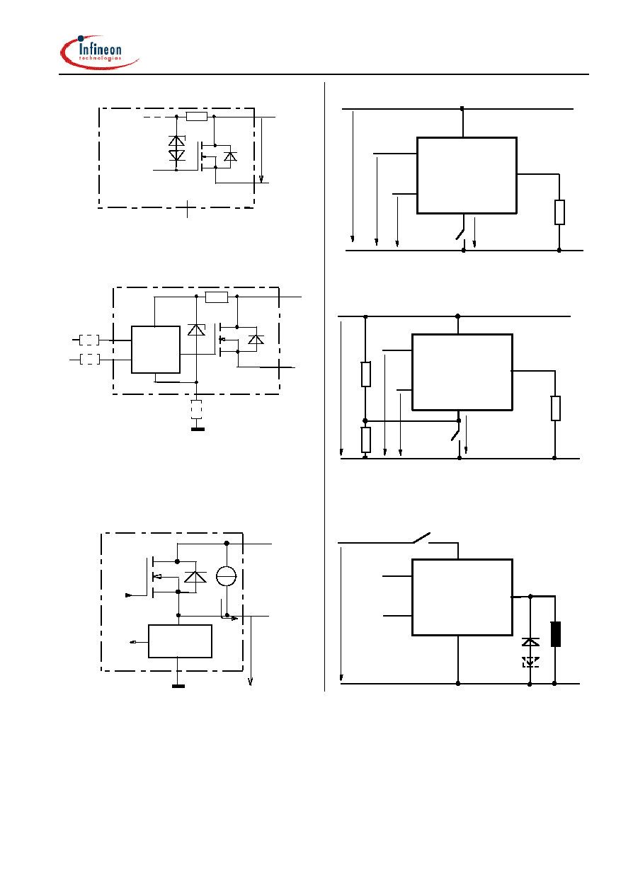
Input circuit (ESD protection)
IN
GND
I
R
ZD
ZD
I
I
I1
I2
ESD-
ZD
I1
6.1 V typ., ESD zener diodes are not designed for
continuous current
Status output
ST
V
Logic
GND
ESD-
ZD
Zener diode: 6.1 V typ., max 5 mA, V
Logic
5 V typ,
ESD zener diodes are not designed for continuous
current
Short Circuit detection
Fault Condition: V
ON
> 8.3 V typ.; IN high
Short circuit
detection
Logic
unit
+ Vbb
OUT
V
ON
BTS 432 I2
Infineon Technologies AG
Page 7
1999-02-19
Inductive and overvoltage output clamp
+ V bb
OUT
GND
VZ
VON
V
ON
clamped to 58 V typ.
Overvolt. and reverse batt. protection
+ V bb
V
OUT
IN
ST
bb
R
Signal GND
Logic
PROFET
VZ
R
GND
GND
IN
R
ST
R
R
bb
= 120
typ
.
, V
Z
+R
bb
*40 mA = 67 V typ., add
R
GND
, R
IN
, R
ST
for extended protection
Open-load detection
OFF-state diagnostic condition: V
OUT
> 3 V typ.; IN low
Open load
detection
Logic
unit
V
OUT
Signal GND
I
L(OL)
OFF
GND disconnect
PROFET
V
IN
ST
OUT
GND
bb
V
bb
1
2
4
3
5
V
IN V ST
VGND
Any kind of load. In case of Input=high is V
OUT
V
IN
- V
IN(T+)
.
Due to V
GND
>0, no V
ST
= low signal available.
GND disconnect with GND pull up
PROFET
V
IN
ST
OUT
GND
bb
V
bb
1
2
4
3
5
V
GND
V
IN
V
ST
Any kind of load. If V
GND >
V
IN
- V
IN(T+)
device stays off
Due to V
GND
>0, no V
ST
= low signal available.
V
bb
disconnect with charged inductive
load
PROFET
V
IN
ST
OUT
GND
bb
V
bb
1
2
4
3
5
high

BTS 432 I2
Infineon Technologies AG
Page 8
1999-02-19
PROFET
V
IN
ST
OUT
GND
bb
V
bb
1
2
4
3
5
high
Inductive Load switch-off energy
dissipation
PROFET
V
IN
ST
OUT
GND
bb
=
E
E
E
EAS
bb
L
R
ELoad
Energy dissipated in PROFET E
AS
= E
bb
+ E
L
- E
R
.
E
Load
< E
L
, E
L
=
1/2
* L * I
2
L

BTS 432 I2
Infineon Technologies AG
Page 9
1999-02-19
Options Overview
all versions: High-side switch, Input protection, ESD protection, load dump and
reverse battery protection , protection against loss of ground
Type
BTS 432D2 432E2 432F2
432I2
Logic version
D
E
F
I
Overtemperature protection
Tj >150 ∞C, latch function
17)18)
Tj >150 ∞C, with auto-restart on cooling
X
X
X
X
Short-circuit to GND protection
switches off when V
ON
>8.3 V typ.
17)
(when first turned on after approx. 200
µ
s)
X
X
X
X
Open load detection
in OFF-state with sensing current 30
µ
A typ.
in ON-state with sensing voltage drop across
power transistor
X
X
X
X
Undervoltage shutdown with auto restart
X
X
X
X
Overvoltage shutdown with auto restart
X
X
X
X
Status feedback for
overtemperature
short circuit to GND
short to V
bb
open load
undervoltage
overvoltage
X
X
-
19)
X
X
X
X
X
-
19)
X
-
-
X
X
-
19)
X
-
-
X
X
X
X
X
X
Status output type
CMOS
Open drain
X
X
X
X
Output negative voltage transient limit
(fast inductive load switch off)
to V
bb
- V
ON(CL)
X
X
X
X
Load current limit
high level
(can handle loads with high inrush currents)
medium level
low level
(better protection of application)
X
X
X
X
17
) Latch except when V
bb
-V
OUT
< V
ON(SC)
after shutdown. In most cases V
OUT
= 0 V after shutdown (V
OUT
0 V only if forced externally). So the device remains latched unless V
bb
< V
ON(SC)
(see page 4). No latch
between turn on and t
d(SC)
.
18)
With latch function. Reseted by a) Input low, b) Undervoltage, c) Overvoltage
19
) Low resistance short V
bb
to output may be detected by no-load-detection

BTS 432 I2
Infineon Technologies AG
Page 10
1999-02-19
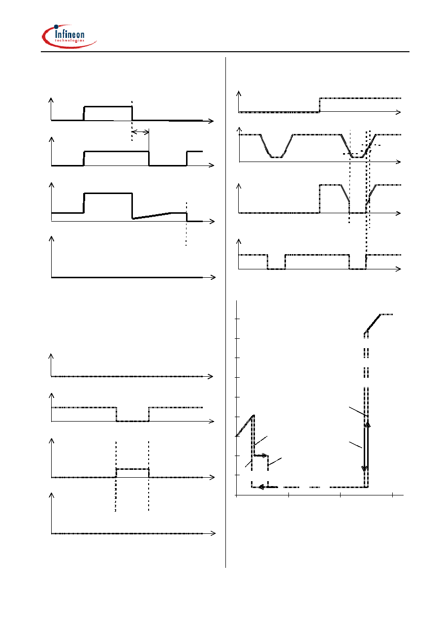
Timing diagrams
Figure 1a: V
bb
turn on:
IN
V
OUT
t
V
ST CMOS
bb
A
A
t d(bb IN)
in case of too early VIN=high the device may not turn on (curve
A)
t
d(bb IN)
approx. 150
µ
s
Figure 2a: Switching a lamp,
IN
ST
OUT
L
t
V
I
Figure 2b: Switching an inductive load
IN
ST
L
t
V
I
OUT
Figure 3a: Turn on into short circuit,
IN
ST
OUT
L
t
V
I
td(SC)
td(SC) approx. 200
µ
s if V
bb
- V
OUT
> 8.3 V typ.

BTS 432 I2
Infineon Technologies AG
Page 11
1999-02-19
Figure 3b: Turn on into overload,
IN
ST
L
t
I
L(SCr)
I
L(SCp)
I
Heating up may require several milliseconds , V
bb
- V
OUT
< 8.3 V
typ.
Figure 3c: Short circuit while on:
IN
ST
OUT
L
t
V
I
**)
**) current peak approx. 20
µ
s
Figure 4a: Overtemperature,
Reset if (IN=low) and (T
j
<T
jt
)
IN
ST
OUT
J
t
V
T
*) ST goes high , when VIN=low and Tj<Tjt
Figure 5a: Open load: detection in ON-state, open
load occurs in on-state
IN
ST
OUT
L
t
V
I
open
normal
normal
t
d(ST OL1)
td(OL ST2)
t
d(ST OL1)
= tbd
µ
s typ., t
d(ST OL2)
= tbd
µ
s typ
BTS 432 I2
Infineon Technologies AG
Page 12
1999-02-19
Figure 5b: Open load: detection in OFF-state, turn
on/off to open load
IN
ST
OUT
L
t
V
I
open
normal
t
d(ST OL3)
*)
in case of external capacity t
d(ST,OL3)
may be higher due to high
impedance *) I
L
=
30
µ
A typ
Figure 5c: Open load: detection in OFF-state, open
load occurs in off-state
IN
ST
OUT
L
t
V
I
open
load
normal
load
normal
load
*)
*)
*) I
L
=
30
µ
A typ
Figure 6a: Undervoltage:
IN
V
OUT
t
V
bb
ST CMOS
V
V
bb(under)
bb(u rst)
bb(u cp)
V
Figure 6b: Undervoltage restart of charge pump
V
ON
[V]
bb(under)
V
V
bb(u rst)
V
bb(over)
V
bb(o rst)
V
bb(u cp)
off
on
off
V
ON(CL)
V
bb
V
on
V
bb
[V]
charge pump starts at V
bb(ucp)
=6.5 V typ.

BTS 432 I2
Infineon Technologies AG
Page 13
1999-02-19
Figure 7a: Overvoltage:
IN
V
OUT
t
V
bb
ST
ON(CL)
V
V
bb(over)
V
bb(o rst)

BTS 432 I2
Infineon Technologies AG
Page 14
1999-02-19
Package and Ordering Code
All dimensions in mm
Standard TO-220AB/5
Ordering code
BTS 432 I2
Q67060-S6204-A2
SMD TO-220AB/5, Opt. E3122
Ordering code
BTS 432 I2 E3122A T&R:
Q67060-S6204-A3

BTS 432 I2
Infineon Technologies AG
Page 15
1999-02-19
Published by Infineon Technologies AG
Balanstraþe 73, D-81541 M¸nchen
©
Infineon Technologies AG 2002. All Rights Reserved
Attention please!
As far as patents or other rights of third parties are concerned,
liability is only assumed for components, not for applications,
processes and circuits implemented within components or
assemblies. The information describes a type of component and
shall not be considered as warranted characteristics. Terms of
delivery and rights to change design reserved. For questions on
technology, delivery and prices please contact Infineon Offices in
Germany or the Infineon Companies and Representatives
worldwide (see address list). Due to technical requirements
components may contain dangerous substances. For information
on the types in question please contact your nearest Infineon
Office. Infineon Technologies AG is an approved CECC
manufacturer.
Packing: Please use the recycling operators known to you. We
can also help you - get in touch with your nearest sales office. By
agreement we will take packing material back, if it is sorted. You
must bear the costs of transport. For packing material that is
returned to us unsorted or which we are not obliged to accept, we
shall have to invoice you for any costs incurred.
Components used in life-support devices or systems must be
expressly authorised for such purpose! Critical components20
)
of Infineon Technologies AG, may only be used in life supporting
devices or systems21
)
with the express written approval of Infineon
Technologies AG.
20) A critical component is a component used in a life-support
device or system whose failure can reasonably be expected
to cause the failure of that life-support device or system, or to
affect its safety or effectiveness of that device or system.
21) Life support devices or systems are intended (a) to be
implanted in the human body or (b) support and/or maintain
and sustain and/or protect human life. If they fail, it is
reasonably to assume that the health of the user or other
persons may be endangered.