HYB 39S64400/800/160BT(L)
64-MBit Synchronous DRAM
Data Book
1
12.99
The HYB 39S64400/800/160BT are four bank Synchronous DRAM's organized as
4 banks
◊
4MBit
◊
4, 4 banks
◊
2 MBit
◊
8 and 4 banks
◊
1 Mbit
◊
16 respectively. These synchron-
ous devices achieve high speed data transfer rates by employing a chip architecture that prefects
multiple bits and then synchronizes the output data to a system clock. The chip is fabricated using
the Infineon advanced 0.2
µ
m 64 MBit DRAM process technology.
The device is designed to comply with all JEDEC standards set for Synchronous DRAM products,
both electrically and mechanically. All of the control, address, data input and output circuits are
synchronized with the positive edge of an externally supplied clock.
Operating the four memory banks in an interleave fashion allows random access operation to occur
at higher rates than is possible with standard DRAMs. A sequential and gapless data rate is
possible depending on burst length, CAS latency and speed grade of the device.
Auto Refresh (CBR) and Self Refresh operation are supported. These devices operates with a
single 3.3 V
±
0.3 V power supply and are available in TSOPII packages.
∑
High Performance:
∑
Fully Synchronous to Positive Clock Edge
∑
0 to 70
∞
C operating temperature
∑
Four Banks controlled by BA0 & BA1
∑
Programmable CAS Latency: 2, 3
∑
Programmable Wrap Sequence: Sequential
or Interleave
∑
Programmable Burst Length: 1, 2, 4, 8
∑
Full page (optional) for sequential wrap
around
∑ Multiple Burst Read with Single Write
Operation
∑ Automatic and Controlled Precharge
Command
∑ Data Mask for Read/Write Control (x4, x8)
∑ Data Mask for Byte Control (x16)
∑ Auto Refresh (CBR) and Self Refresh
∑ Suspend Mode and Power Down Mode
∑ 4096 Refresh Cycles / 64 ms
∑ Random Column Address every CLK
(1-N Rule)
∑ Single 3.3 V
±
0.3 V Power Supply
∑ LVTTL Interface
∑ Plastic Packages:
P-TSOPII-54 400mil width (x4, x8, x16)
∑ -7.5 version for PC133 3-3-3 application
-8 version for PC100 2-2-2 applications
-7.5
-8
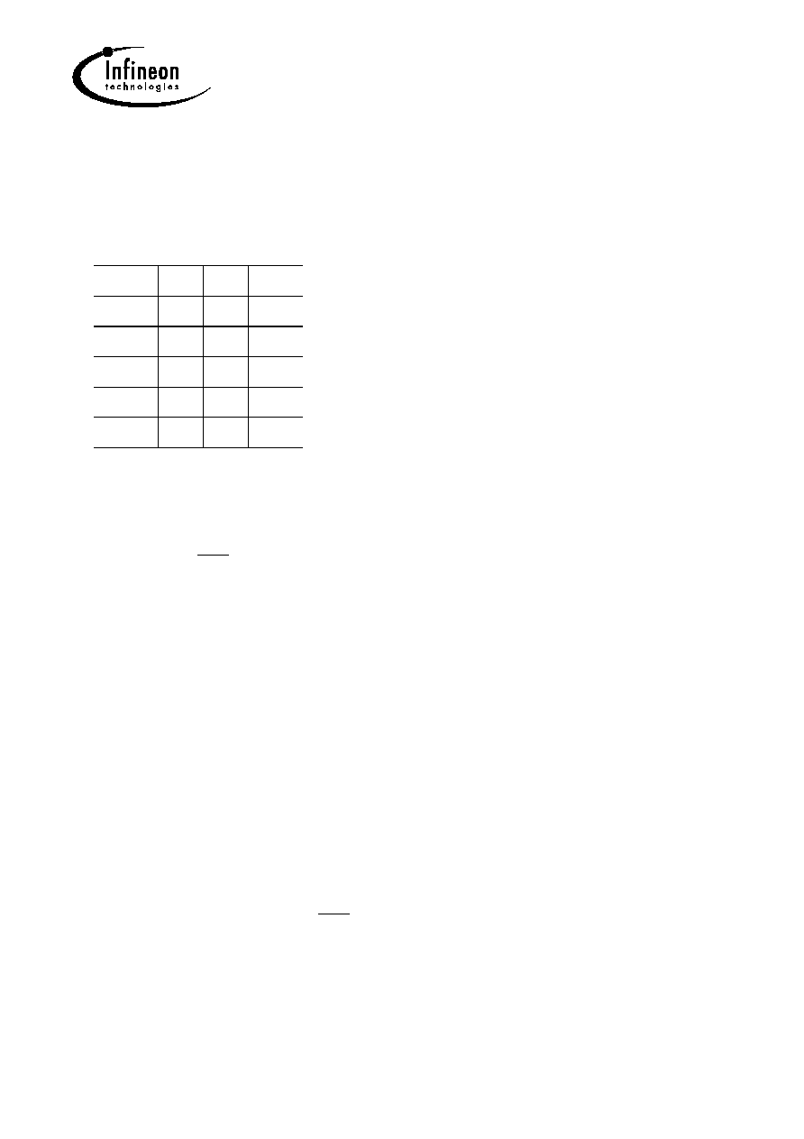
Units
f
CKMAX
133
125
MHz
t
CK3
7.5
8
ns
t
AC3
5.4
6
ns
t
CK2
10
10
ns
t
AC2
6
6
ns
64-MBit Synchronous DRAM
HYB 39S64400/800/160BT(L)
64-MBit Synchronous DRAM
Data Book
2
12.99
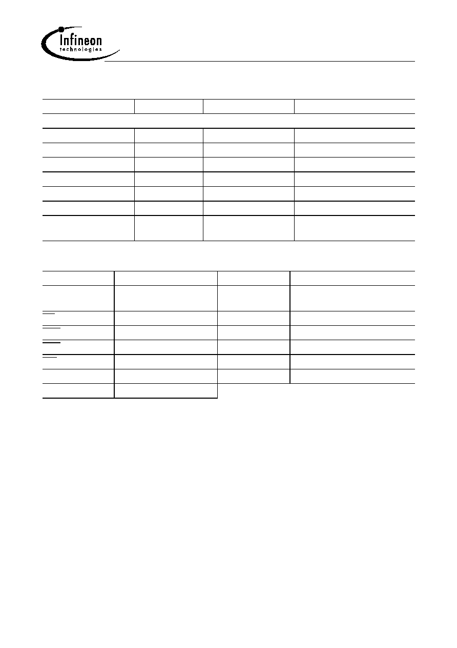
Ordering Information
Type
Ordering Code
Package
Description
HYB 39S64400BT-7.5
Q67100-Q2781
P-TSOP-54-2 (400mil) 133MHz 4B
◊
4M x4 SDRAM
HYB 39S64400BT-8
Q67100-Q1838
P-TSOP-54-2 (400mil) 125MHz 4B
◊
4M x4 SDRAM
HYB 39S64800BT-7.5
Q67100-Q2776
P-TSOP-54-2 (400mil) 133MHz 4B
◊
2M x8 SDRAM
HYB 39S64800BT-8
Q67100-Q1841
P-TSOP-54-2 (400mil) 125MHz 4B
◊
2M x8 SDRAM
HYB 39S64160BT-7.5
Q67100-Q2800
P-TSOP-54-2 (400mil) 133MHz 4B
◊
1M x16 SDRAM
HYB 39S64160BT-8
Q67100-Q1844
P-TSOP-54-2 (400mil) 125MHz 4B
◊
1M x16 SDRAM
HYB 39S64xxx0BTL-
7.5/-8
on request
P-TSOP-54-2 (400mil) Low Power (L-versions)
Pin Definitions and Functions
CLK
Clock Input
DQ
Data Input/Output
CKE
Clock Enable
DQM, LDQM,
UDQM
Data Mask
CS
Chip Select
V
DD
Power (+ 3.3 V)
RAS
Row Address Strobe
V
SS
Ground
CAS
Column Address Strobe
V
DDQ
Power for DQ's (+ 3.3 V)
WE
Write Enable
V
SSQ
Ground for DQ's
A0 - A11
Address Inputs
N.C.
Not connected
BA0, BA1
Bank Select
HYB 39S64400/800/160BT(L)
64-MBit Synchronous DRAM
Data Book
3
12.99
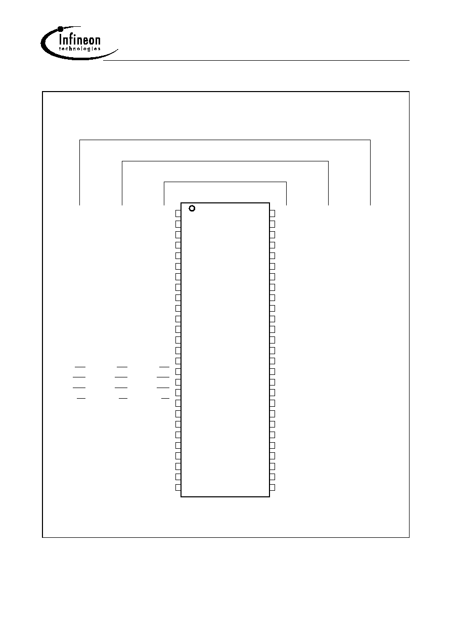
Pin Configuration for x4, x8 & x16 Organized 64M-SDRAMs
TSOPII-54 (10.16 mm
◊
22.22 mm, 0.8 mm pitch)
SPP03695
20
28
19
17
18
16
15
N.C.
N.C.
N.C.
DDQ
V
9
10
12
11
2
3
4
5
1
13
40
32
31
30
29
36
37
38
39
35
34
7
6
8
33
14
N.C.
N.C.
N.C.
N.C.
WE
A6
A5
A4
A3
A2
A0
22
21
CKE
A1
23
24
25
SS
V
46
47
48
50
49
42
43
44
45
41
CLK
DQM
A7
A8
A9
N.C.
CAS
RAS
CS
BA0
A10
SSQ
V
N.C.
SS
V
DDQ
V
V
SSQ
V
DDQ
SSQ
V
N.C.
DD
V
N.C.
V
DDQ
V
SS
V
DD
26
27
51
52
54
53
BA1
DQ1
N.C.
DQ0
DD
N.C.
V
A11
DQ2
N.C.
DQ3
V
SSQ
V
A10
A0
A3
A2
DD
A1
V
DD
N.C.
BA0
BA1
CS
RAS
CAS
WE
V
SSQ
N.C.
DQ2
DDQ
N.C.
DQ3
SSQ
N.C.
V
V
DD
DQ0
DDQ
N.C.
DQ1
V
V
V
CAS
A10
A3
DD
V
A1
A2
A0
RAS
BA0
BA1
CS
WE
LDQM
DD
DQ2
V
V
V
V
DQ5
DQ7
SSQ
DQ6
DQ4
DDQ
DQ3
SSQ
DQ1
DQ0
DDQ
DD
V
V
A8
A4
V
SS
A7
A5
A6
CKE
A11
N.C.
A9
DQM
N.C.
CLK
SS
V
N.C.
DQ4
V
N.C.
DDQ
N.C.
DQ5
V
SSQ
DDQ
DQ7
V
N.C.
DQ6
SSQ
V
SS
V
CLK
UDQM
N.C.
A11
CKE
A8
A4
V
SS
A6
A5
A7
A9
SS
DQ15
DQ13
DQ11
DQ9
SSQ
DQ14
DDQ
SSQ
DQ12
DDQ
DQ8
DQ10
V
V
V
V
V
SS
16M x 4
8M x 8
4M x 16
N.C.
N.C.
HYB 39S64400/800/160BT(L)
64-MBit Synchronous DRAM
Data Book
4
12.99
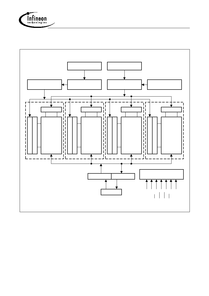
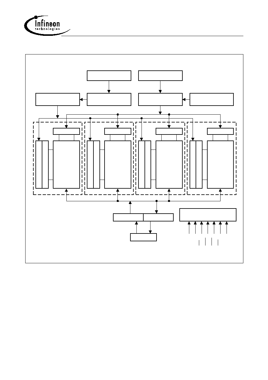
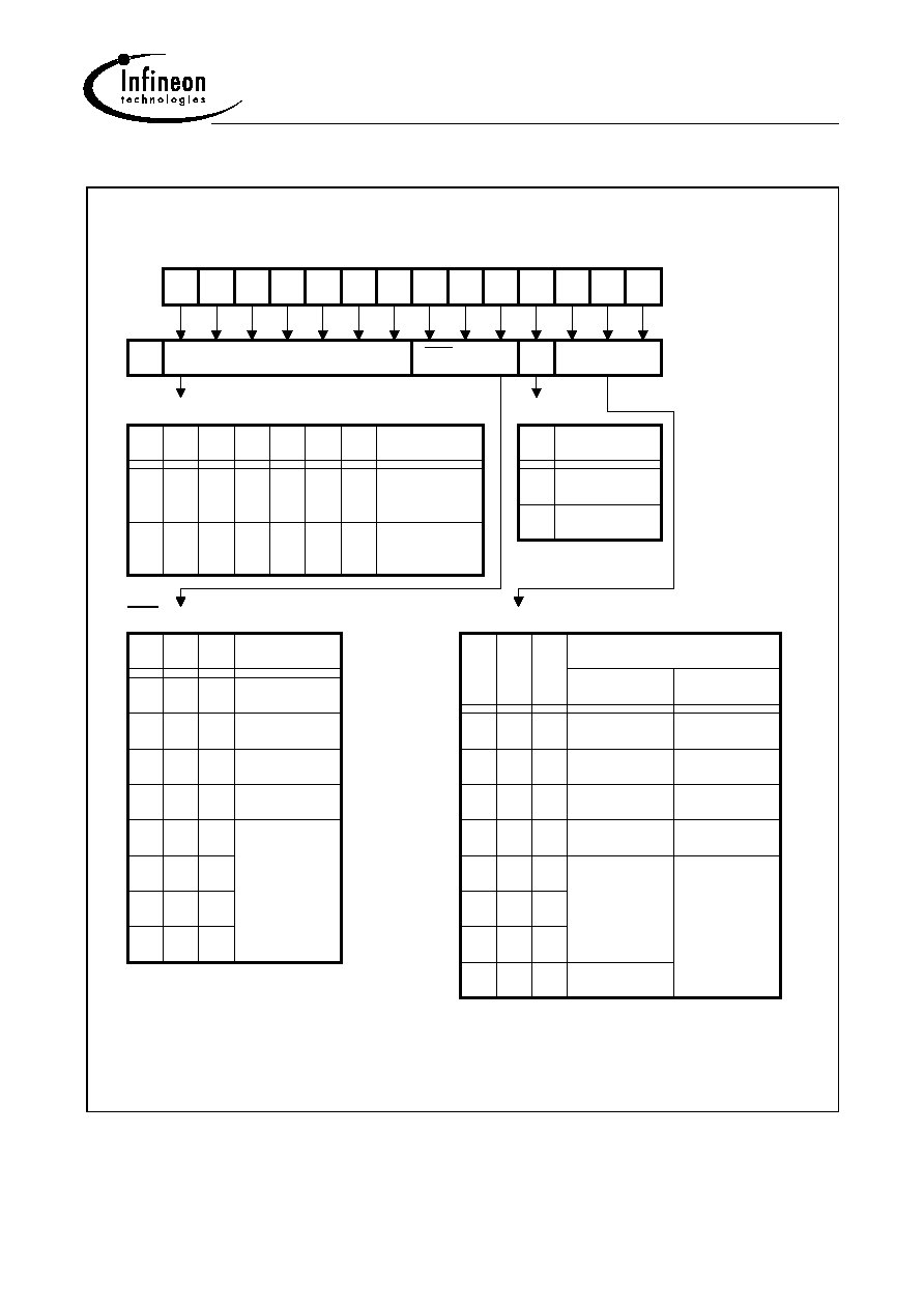
Functional Block Diagrams
Block Diagram: 4 Bank
◊
4M
◊
4 SDRAM
SPB03696
Memory
Bank 0
4096 x 1024
x 4 Bit
Column Decoder
Sense Amplifier & I(O) Bus
Row Decoder
Array
Column Decoder
Bank 1
Array
Memory
4096 x 1024
Row Decoder
Column Decoder
Bank 2
Array
Memory
4096 x 1024
Row Decoder
Column Decoder
Bank 3
Array
Memory
4096 x 1024
Row Decoder
Counter
Column Address
Column Address
Buffer
A0 - A9, AP, BA0, BA1
Column Addresses
Row Address
Buffer
A0 - A11, BA0, BA1
Row Addresses
Refresh Counter
DQ0 - DQ3
Input Buffer
Output Buffer
Timing Generator
Control Logic &
CLK
CKE
CS
RAS
CAS
WE
DQM
Sense Amplifier & I(O) Bus
x 4 Bit
Sense Amplifier & I(O) Bus
x 4 Bit
Sense Amplifier & I(O) Bus
x 4 Bit
HYB 39S64400/800/160BT(L)
64-MBit Synchronous DRAM
Data Book
5
12.99
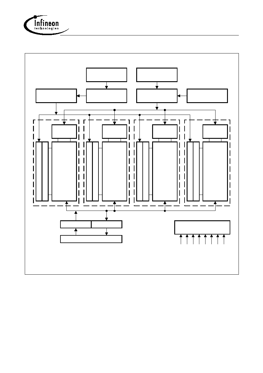
Block Diagram: 4 Bank
◊
2M
◊
8 SDRAM
SPB03697
Memory
Bank 0
4096 x 512
x 8 Bit
Column Decoder
Sense Amplifier & I(O) Bus
Row Decoder
Array
Column Decoder
Bank 1
Array
Memory
Row Decoder
Column Decoder
Bank 2
Array
Memory
Row Decoder
Column Decoder
Bank 3
Array
Memory
Row Decoder
Counter
Column Address
Column Address
Buffer
A0 - A8, AP, BA0, BA1
Column Addresses
Row Address
Buffer
A0 - A11, BA0, BA1
Row Addresses
Refresh Counter
DQ0 - DQ7
Input Buffer
Output Buffer
Timing Generator
Control Logic &
CLK
CKE
CS
RAS
CAS
WE
DQM
4096 x 512
4096 x 512
4096 x 512
Sense Amplifier & I(O) Bus
x 8 Bit
Sense Amplifier & I(O) Bus
x 8 Bit
Sense Amplifier & I(O) Bus
x 8 Bit
HYB 39S64400/800/160BT(L)
64-MBit Synchronous DRAM
Data Book
6
12.99
Block Diagram: 4 Bank
◊
1M
◊
16 SDRAM
Memory
Array
Bank 1
4096 x 256
x 16 Bit
Memory
Array
Bank 2
4096 x 256
x 16 Bit
Memory
Array
Bank 3
4096 x 256
x 16 Bit
SPB04120
Column Address
Counter
Row
Decoder
Memory
Array
Bank 0
4096 x 256
x 16 Bit
Column Decoder
Sense amplifier & I(O) Bus
Row
Decoder
Sense amplifier & I(O) Bus
Row
Decoder
Row
Decoder
Column Decoder
Sense amplifier & I(O) Bus
Row Address
Buffer
Column Address
Buffer
Refresh Counter
Sense amplifier & I(O) Bus
A0 - A11,
BA0, BA1
A0 - A7, AP,
BA0, BA1
Column Addresses
Row Addresses
Input Buffer
Output Buffer
DQ0 - DQ15
Control Logic &
Timing Generator
CLK
CKE
CS
RAS
CAS
WE
DQMU
DQML
Column Decoder
Column Decoder
HYB 39S64400/800/160BT(L)
64-MBit Synchronous DRAM
Data Book
7
12.99
Signal Pin Description
Pin
Type
Signal Polarity Function
CLK
Input
Pulse
Positive
Edge
The System Clock Input. All of the SDRAM inputs are
sampled on the rising edge of the clock.
CKE
Input
Level
Active
High
Activates the CLK signal when high and deactivates the
CLK signal when low, thereby initiates either the Power
Down mode, Suspend mode, or the Self Refresh mode.
CS
Input
Pulse
Active
Low
CS enables the command decoder when low and disables
the command decoder when high. When the command
decoder is disabled, new commands are ignored but
previous operations continue.
RAS
CAS
WE
Input
Pulse
Active
Low
When sampled at the positive rising edge of the clock,
CAS, RAS, and WE define the command to be executed by
the SDRAM.
A0 - A11
Input
Level
≠
During a Bank Activate command cycle, A0 - A11 define
the row address (RA0 - RA11) when sampled at the rising
clock edge.
During a Read or Write command cycle, A0-An define the
column address (CA0 - CAn) when sampled at the rising
clock edge.CAn depends from the SDRAM organization:
16M
◊
4 SDRAM CAn = CA9
(Page Length = 1024 bits)
8M
◊
8 SDRAM
CAn = CA8
(Page Length = 512 bits)
4M
◊
16 SDRAM CAn = CA7
(Page Length = 256 bits)
In addition to the column address, A10 (= AP) is used to
invoke autoprecharge operation at the end of the burst read
or write cycle. If A10 is high, autoprecharge is selected and
BA0, BA1 defines the bank to be precharged. If A10 is low,
autoprecharge is disabled.
During a Precharge command cycle, A10 (= AP) is used in
conjunction with BA0 and BA1 to control which bank(s) to
precharge. If A10 is high, all four banks will be precharged
regardless of the state of BA0 and BA1. If A10 is low, then
BA0 and BA1 are used to define which bank to precharge.
BA0, BA1 Input
Level
≠
Bank Select Inputs. Selects which bank is to be active.
DQx
Input
Output
Level
≠
Data Input/Output pins operate in the same manner as on
conventional DRAMs.
HYB 39S64400/800/160BT(L)
64-MBit Synchronous DRAM
Data Book
8
12.99
DQM
LDQM
UDQM
Input
Pulse
Active
High
The Data Input/Output mask places the DQ buffers in a
high impedance state when sampled high. In Read mode,
DQM has a latency of two clock cycles and controls the
output buffers like an output enable. In Write mode, DQM
has a latency of zero and operates as a word mask by
allowing input data to be written if it is low but blocks the
write operation if DQM is high.
One DQM input it present in
◊
4 and
◊
8 SDRAMs, LDQM
and UDQM controls the lower and upper bytes in
◊
16
SDRAMs.
V
DD
V
SS
Supply ≠
≠
Power and ground for the input buffers and the core logic.
V
DDQ
V
SSQ
Supply ≠
≠
Isolated power supply and ground for the output buffers to
provide improved noise immunity.
V
REF
Input
Level
≠
Reference voltage for SDRAM versions supporting SSTL
interface
Signal Pin Description (cont'd)
Pin
Type
Signal Polarity Function
HYB 39S64400/800/160BT(L)
64-MBit Synchronous DRAM
Data Book
9
12.99
Operation Definition
All of SDRAM operations are defined by states of control signals CS, RAS, CAS, WE, and DQM at
the positive edge of the clock. The following list shows the truth table for the operation commands.
Notes
1. V = Valid, x = Don't Care, L = Low Level, H = High Level
2. CKEn signal is input level when commands are provided, CKEn-1 signal is input level one clock
before the commands are provided.
3. This is the state of the banks designated by BA0, BA1 signals.
4. Device state is Full Page Burst operation
5. Power Down Mode can not entry in the burst cycle. When this command assert in the burst mode
cycle device is clock suspend mode.
Operation
Device
State
CKE
n-1
CKE
n
CS
RAS
CAS
WE
DQM A0-9,
A11
A10
BA0
BA1
Row Activate (ACT)
Idle
3
H
X
L
L
H
H
X
V
V
V
Read (READ)
Active
3
H
X
L
H
L
H
X
V
L
V
Read w/ Autoprecharge
(READA)
Active
3
H
X
L
H
L
H
X
V
H
V
Write (WRITE)
Active
3
H
X
L
H
L
L
X
V
L
V
Write w/ Autoprecharge
(WRITEA)
Active
3
H
X
L
H
L
L
X
V
H
V
Row Precharge (PRE)
Any
H
X
L
L
H
L
X
X
L
V
Precharge All (PREA)
Any
H
X
L
L
H
L
X
X
H
X
Mode Register Set (MRS)
Idle
H
X
L
L
L
L
X
V
V
V
No Operation (NOP)
Any
H
X
L
H
H
H
X
X
X
X
Device Deselect (INHBT)
Any
H
X
H
X
X
X
X
X
X
X
Auto Refresh (REFA)
Idle
H
H
L
L
L
H
X
X
X
X
Self Refresh Entry (REFS-EN) Idle
H
L
L
L
L
H
X
X
X
X
Self Refresh Exit (REFS-EX)
Idle
(Self
Refr.)
L
H
H
X
X
X
X
X
X
X
L
H
H
X
Power Down Entry (PDN-EN) Idle
Active
5
H
L
H
X
X
X
X
X
X
X
L
H
H
X
Power Down Exit (PDN-EX)
Any
(Power
Down)
L
H
H
X
X
X
X
X
X
X
L
H
H
L
Data Write/Output Enable
Active
H
X
X
X
X
X
L
X
X
X
Data Write/Output Disable
Active
H
X
X
X
X
X
H
X
X
X
HYB 39S64400/800/160BT(L)
64-MBit Synchronous DRAM
Data Book
10
12.99
BA1 BA0 A11 A10 A9
A8
A7
A6
A5
A4
A3
A2
A1
A0
Operation Mode
CAS Latency
BT
Burst Length
Address Bus (Ax)
Mode Register (Mx)
Operation Mode
BA0
BA1
M8
M10
M11
M9
M7
Mode
burst read /
burst write
0
0
0
0
0
0
0
single write
burst read /
0
0
0
1
0
0
0
Burst Type
M3
Type
Sequential
Interleave
0
1
M6
M5
M4
Latency
CAS Latency
0
0
0
Reserved
0
0
1
Reserved
0
1
0
2
0
1
1
3
1
0
0
1
0
1
1
1
0
Reserved
1
1
1
Address Input for Mode Set (Mode Register Operation)
1
1
1
1
0
0
0
0
M2
1
2
Reserved
0
0
1
1
1
0
0
1
1
0
1
1
1
0
0
M1
0
M0
8
4
Length
Burst Length
Sequential
Interleave
Reserved
Full Page*)
1
2
4
8
SPS03409
*) optional

HYB 39S64400/800/160BT(L)
64-MBit Synchronous DRAM
Data Book
11
12.99
Power On and Initialization
The default power on state of the mode register is supplier specific and may be undefined. The
following power on and initialization sequence guarantees the device is preconditioned to each
users specific needs. Like a conventional DRAM, the Synchronous DRAM must be powered up and
initialized in a predefined manner.During power on, all
V
DD
and
V
DDQ
pins must be built up
simultaneously to the specified voltage when the input signals are held in the "NOP" state. The
power on voltage must not exceed
V
DD
+ 0.3 V on any of the input pins or
V
DD
supplies. The CLK
signal must be started at the same time. After power on, an initial pause of 200
µ
s is required
followed by a precharge of both banks using the precharge command. To prevent data contention
on the DQ bus during power on, it is required that the DQM and CKE pins be held high during the
initial pause period. Once all banks have been precharged, the Mode Register Set Command must
be issued to initialize the Mode Register. A minimum of eight Auto Refresh cycles (CBR) are also
required.These may be done before or after programming the Mode Register. Failure to follow these
steps may lead to unpredictable start-up modes.
Programming the Mode Register
The Mode register designates the operation mode at the read or write cycle. This register is divided
into 4 fields. A Burst Length Field to set the length of the burst, an Addressing Selection bit to
program the column access sequence in a burst cycle (interleaved or sequential), a CAS Latency
Field to set the access time at clock cycle and a Operation mode field to differentiate between
normal operation (Burst read and burst Write) and a special Burst Read and Single Write mode. The
mode set operation must be done before any activate command after the initial power up. Any
content of the mode register can be altered by re-executing the mode set command. All banks must
be in precharged state and CKE must be high at least one clock before the mode set operation. After
the mode register is set, a Standby or NOP command is required. Low signals of RAS, CAS, and
WE at the positive edge of the clock activate the mode set operation. Address input data at this
timing defines parameters to be set as shown in the previous table.
Read and Write Operation
When RAS is low and both CAS and WE are high at the positive edge of the clock, a RAS cycle
starts. According to address data, a word line of the selected bank is activated and all of sense
amplifiers associated to the wordline are set. A CAS cycle is triggered by setting RAS high and CAS
low at a clock timing after a necessary delay,
t
RCD
, from the RAS timing. WE is used to define either
a read (WE = H) or a write (WE = L) at this stage.
SDRAM provides a wide variety of fast access modes. In a single CAS cycle, serial data read or
write operations are allowed at up to a 133 MHz data rate. The numbers of serial data bits are the
burst length programmed at the mode set operation, i.e., one of 1, 2, 4, 8 and full page, where full
page is an optional feature in this device. Column addresses are segmented by the burst length and
serial data accesses are done within this boundary. The first column address to be accessed is
supplied at the CAS timing and the subsequent addresses are generated automatically by the
programmed burst length and its sequence. For example, in a burst length of 8 with interleave
sequence, if the first address is `2', then the rest of the burst sequence is 3, 0, 1, 6, 7, 4, and 5.
Full page burst operation is only possible using the sequential burst type and page length is a
function of the I/O organization and column addressing. Full page burst operation do not self

HYB 39S64400/800/160BT(L)
64-MBit Synchronous DRAM
Data Book
12
12.99
terminate once the burst length has been reached. In other words, unlike burst length of 2, 3 or 8,
full page burst continues until it is terminated using another command.
Similar to the page mode of conventional DRAM's, burst read or write accesses on any column
address are possible once the RAS cycle latches the sense amplifiers. The maximum
t
RAS
or the
refresh interval time limits the number of random column accesses. A new burst access can be
done even before the previous burst ends. The interrupt operation at every clock cycle is supported.
When the previous burst is interrupted, the remaining addresses are overridden by the new address
with the full burst length. An interrupt which accompanies an operation change from a read to a write
is possible by exploiting DQM to avoid bus contention.
When two or more banks are activated sequentially, interleaved bank read or write operations are
possible. With the programmed burst length, alternate access and precharge operations on two or
more banks can realize fast serial data access modes among many different pages. Once two or
more banks are activated, column to column interleave operation can be done between different
pages.
Refresh Mode
SDRAM has two refresh modes, Auto Refresh and Self Refresh. Auto Refresh is similar to the CAS
-before-RAS refresh of conventional DRAMs. All of banks must be precharged before applying any
refresh mode. An on-chip address counter increments the word and the bank addresses and no
bank information is required for both refresh modes.
The chip enters the Auto Refresh mode, when RAS and CAS are held low and CKE and WE are
held high at a clock timing. The mode restores word line after the refresh and no external precharge
Burst Length and Sequence
Burst
Length
Starting
Address
(A2 A1 A0)
Sequential Burst Addressing
(decimal)
Interleave Burst
Addressing
(decimal)
2
xx0
xx1
0, 1
1, 0
0, 1
1, 0
4
x00
x01
x10
x11
0, 1, 2, 3
1, 2, 3, 0
2, 3, 0, 1
3, 0, 1, 2
0, 1, 2, 3
1, 0, 3, 2
2, 3, 0, 1
3, 2, 1, 0
8
000
001
010
011
100
101
110
111
0 1 2 3 4 5 6 7
1 2 3 4 5 6 7 0
2 3 4 5 6 7 0 1
3 4 5 6 7 0 1 2
4 5 6 7 0 1 2 3
5 6 7 0 1 2 3 4
6 7 0 1 2 3 4 5
7 0 1 2 3 4 5 6
0 1 2 3 4 5 6 7
1 0 3 2 5 4 7 6
2 3 0 1 6 7 4 5
3 2 1 0 7 6 5 4
4 5 6 7 0 1 2 3
5 4 7 6 1 0 3 2
6 7 4 5 2 3 0 1
7 6 5 4 3 2 1 0
Full Page
(optional)
nnn
Cn, Cn+1, Cn+2,.....
not supported

HYB 39S64400/800/160BT(L)
64-MBit Synchronous DRAM
Data Book
13
12.99
command is necessary. A minimum
t
RC
time is required between two automatic refreshes in a burst
refresh mode. The same rule applies to any access command after the automatic refresh operation.
The chip has an on-chip timer and the Self Refresh mode is available. It enters the mode when RAS,
CAS, and CKE are low and WE is high at a clock timing. All of external control signals including the
clock are disabled. Returning CKE to high enables the clock and initiates the refresh exit operation.
After the exit command, at least one
t
RC
delay is required prior to any access command.
DQM Function
DQM has two functions for data I/O read and write operations. During reads, when it turns to "high"
at a clock timing, data outputs are disabled and become high impedance after two clock delay (DQM
Data Disable Latency
t
DQZ
). It also provides a data mask function for writes. When DQM is activated,
the write operation at the next clock is prohibited (DQM Write Mask Latency
t
DQW
= zero clocks).
Suspend Mode
During normal access mode, CKE is held high enabling the clock. When CKE is low, it freezes the
internal clock and extends data read and write operations. One clock delay is required for mode
entry and exit (Clock Suspend Latency
t
CSL
).
Power Down
In order to reduce standby power consumption, a power down mode is available. All banks must be
precharged and the necessary Precharge delay (
t
RP
) must occur before the SDRAM can enter the
Power Down mode. Once the Power Down mode is initiated by holding CKE low, all of the receiver
circuits except CLK and CKE are gated off. The Power Down mode does not perform any refresh
operations, therefore the device can't remain in Power Down mode longer than the Refresh period
(
t
REF
) of the device. Exit from this mode is performed by taking CKE "high". One clock delay is
required for mode entry and exit.
Auto Precharge
Two methods are available to precharge SDRAMs. In an automatic precharge mode, the CAS
timing accepts one extra address, CA10, to determine whether the chip restores or not after the
operation. If CA10 is high when a Read Command is issued, the Read with Auto-Precharge
function is initiated. If CA10 is high when a Write Command is issued, the Write with Auto-
Precharge function is initiated. The SDRAM automatically enters the precharge operation two
clocks after the last data in.
Precharge Command
There is also a separate precharge command available. When RAS and WE are low and CAS is
high at a clock timing, it triggers the precharge operation. Three address bits, BA0, BA1 and A10 are
used to define banks as shown in the following list. The precharge command can be imposed one
clock before the last data out for CAS latency = 2 and two clocks before the last data out for CAS
latency = 3. Writes require a time delay
t
WR
from the last data out to apply the precharge command.

HYB 39S64400/800/160BT(L)
64-MBit Synchronous DRAM
Data Book
14
12.99
Burst Termination
Once a burst read or write operation has been initiated, there are several methods in which to
terminate the burst operation prematurely. These methods include using another Read or Write
Command to interrupt an existing burst operation, use a Precharge Command to interrupt a burst
cycle and close the active bank, or using the Burst Stop Command to terminate the existing burst
operation but leave the bank open for future Read or Write Commands to the same page of the
active bank. When interrupting a burst with another Read or Write Command care must be taken to
avoid DQ contention. The Burst Stop Command, however, has the fewest restrictions making it the
easiest method to use when terminating a burst operation before it has been completed. If a Burst
Stop command is issued during a burst write operation, then any residual data from the burst write
cycle will be ignored. Data that is presented on the DQ pins before the Burst Stop Command is
registered will be written to the memory.
A10
BA0
BA1
0
0
0
Bank 0
0
0
1
Bank 1
0
1
0
Bank 2
0
1
1
Bank 3
1
x
x
all Banks

HYB 39S64400/800/160BT(L)
64-MBit Synchronous DRAM
Data Book
15
12.99
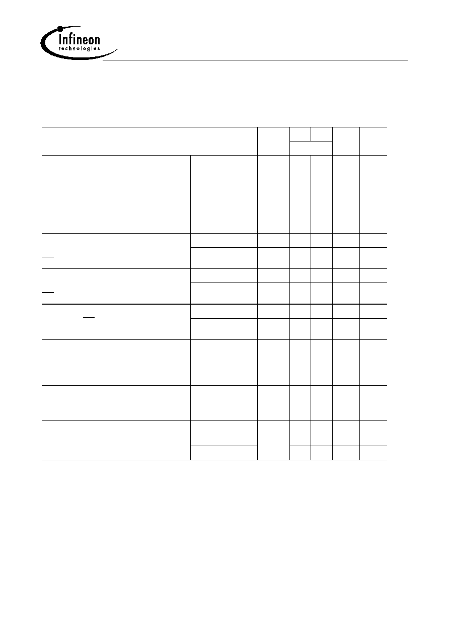
Electrical Characteristics
Absolute Maximum Ratings
Operating Temperature Range .......................................................................................0 to + 70
∞
C
Storage Temperature Range .................................................................................. ≠ 55 to + 150
∞
C
Input/Output Voltage ......................................................................................... ≠ 0.3 to
V
DD
+ 0.3 V
Power Supply Voltage
V
DD
/
V
DDQ
.............................................................................. ≠ 0.3 to + 4.6 V
Power Dissipation ....................................................................................................................... 1 W
Data Out Current (short circuit)............................................................................................... 50 mA
Note: Stresses above those listed under "Absolute Maximum Ratings" may cause permanent
damage of the device. Exposure to absolute maximum rating conditions for extended
periods may affect device reliability.
Notes
1. All voltages are referenced to
V
SS
2.
V
IH
may overshoot to
V
DD
+ 2.0 V for pulse width of < 4 ns with 3.3 V.
V
IL
may undershoot to
≠ 2.0 V for pulse width < 4.0 ns with 3.3 V. Pulse width measured at 50% points with amplitude
measured peak to DC reference.
Recommended Operation and DC Characteristics
T
A
= 0 to 70
∞
C;
V
SS
= 0 V;
V
DD
,
V
DDQ
= 3.3 V
±
0.3 V
Parameter
Symbol
Limit Values
Unit
Notes
min.
max.
Input High Voltage
V
IH
2.0
V
DD
+ 0.3
V
1, 2
Input Low Voltage
V
IL
≠ 0.3
0.8
V
1, 2
Output High Voltage (
I
OUT
= ≠ 4.0 mA)
V
OH
2.4
≠
V
≠
Output Low Voltage (
I
OUT
= 4.0 mA)
V
OL
≠
0.4
V
≠
Input Leakage Current, any input
(0 V <
V
IN
<
V
DDQ
, all other inputs = 0 V)
I
I(L)
≠ 5
5
µ
A
≠
Output Leakage Current
(DQ is disabled, 0 V <
V
OUT
<
V
DD
)
I
O(L)
≠ 5
5
µ
A
≠
Capacitance
T
A
= 0 to 70
∞
C;
V
DD
= 3.3 V
±
0.3 V,
f
= 1 MHz
Parameter
Symbol
Values
Unit
min.
max.
Input Capacitance (CLK)
C
I1
2.5
3.5
pF
Input Capacitance
(A0 - A11, BA0, BA1, RAS, CAS, WE, CS, CKE, DQM)
C
I2
2.5
3.8
pF
Input/Output Capacitance (DQ)
C
IO
4.0
6.0
pF
HYB 39S64400/800/160BT(L)
64-MBit Synchronous DRAM
Data Book
16
12.99
Notes
3. These parameters depend on the cycle rate and these values are measured at 133 MHz for -7.5,
and at 100 MHz for -8 components. Input signals are changed once during
t
CK
, excepts for
I
CC6
and for standby currents when
t
CK
= infinity.
4. These parameters are measured with continuous data stream during read access and all DQ
toggling. CL = 3 and BL = 4 is assumed and the
V
DDQ
current is excluded.
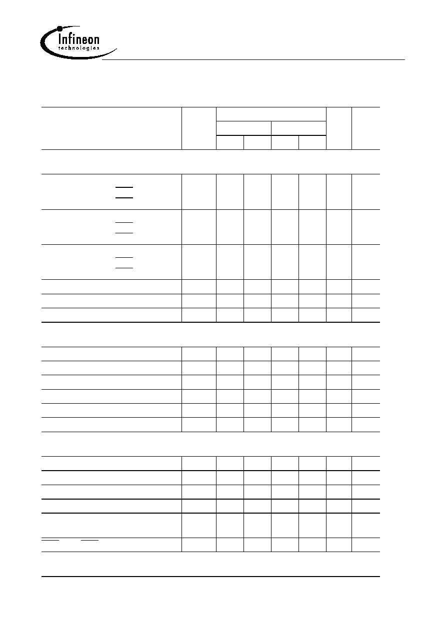
Operating Currents
T
A
= 0 to 70
∞
C,
V
DD
= 3.3 V
±
0.3 V
(Recommended Operating Conditions unless otherwise noted)
Parameter & Test Condition
Symb. -7.5 -8
Unit
Note
max.
Operating Current
t
RC
=
t
RC(MIN.)
,
t
CK
=
t
CK(MIN.)
Outputs open, Burst Length = 4, CL=3
All banks operated in random access,
all banks operated in ping-pong
manner to maximize gapless data
access
≠
I
CC1
x4
x8
x16
110
120
140
100
110
130
mA
mA
mA
3
Precharge Standby Current
in Power Down Mode
CS =
V
IH (MIN.)
, CKE
V
IL(MAX.)
t
CK
= min
I
CC2P
2
2
mA
3
t
CK
= infinity
I
CC2PS
1
1
mA
3
Precharge Standby Current
in Non-Power Down Mode
CS =
V
IH (MIN.)
, CKE
V
IH(MIN.)
t
CK
= min
I
CC2N
40
35
mA
3
t
CK
= infinity
I
CC2NS
5
5
mA
3
No Operating Current
t
CK
= min., CS =
V
IH (MIN.)
,
active state (max. 4 banks)
CKE
V
IH(MIN.)
I
CC3N
50
45
mA
3
CKE
V
IL(MAX.)
I
CC3P
8
8
mA
3
Burst Operating Current
t
CK
= min
Read command cycling
≠
I
CC4
x4
x8
x16
70
80
110
60
70
100
mA
mA
mA
3, 4
Auto Refresh Current
t
CK
= min
Auto Refresh command cycling
≠
I
CC5
140 130 mA
3
Self Refresh Current
Self Refresh Mode
CKE = 0.2 V
standard
version
I
CC6
1
1
mA
3
L-version
400 400
µ
A
3
HYB 39S64400/800/160BT(L)
64-MBit Synchronous DRAM
Data Book
17
12.99
AC Characteristics
1, 2
T
A
= 0 to 70
∞
C;
V
SS
= 0 V;
V
DD
= 3.3 V
±
0.3 V,
t
T
= 1 ns
Parameter
Symb.
Limit Values
Unit
Note
-7.5
-8
min.
max.
min.
max.
Clock and Clock Enable
Clock Cycle Time
CAS Latency = 3
CAS Latency = 2
t
CK
7.5
10
≠
≠
8
10
≠
≠
ns
ns
≠
Clock Frequency
CAS Latency = 3
CAS Latency = 2
t
CK
133
100
≠
≠
≠
≠
125
100
MHz
MHz
≠
Access Time from Clock
CAS Latency = 3
CAS Latency = 2
t
AC
≠
≠
5.4
6
≠
≠
6
6
ns
ns
2, 3
Clock High Pulse Width
t
CH
2.5
≠
3
≠
ns
≠
Clock Low Pulse Width
t
CL
2.5
≠
3
≠
ns
≠
Transition Time
t
T
0.3
1.2
0.5
10
ns
≠
Setup and Hold Times
Input Setup Time
t
IS
1.5
≠
2
≠
ns
4
Input Hold Time
t
IH
0.8
≠
1
≠
ns
4
CKE Setup Time
t
CKS
1.5
≠
2
≠
ns
4
CKE Hold Time
t
CKH
0.8
≠
1
≠
ns
4
Mode Register Set-up Time
t
RSC
2
≠
2
≠
CLK
≠
Power Down Mode Entry Time
t
SB
0
7
0
8
ns
≠
Common Parameters
Row to Column Delay Time
t
RCD
20
≠
20
≠
ns
5
Row Precharge Time
t
RP
20
≠
20
≠
ns
5
Row Active Time
t
RAS
45
100k
48
100k
ns
5
Row Cycle Time
t
RC
67
≠
70
≠
ns
5
Activate(a) to Activate(b) Command
Period
t
RRD
14
≠
16
≠
ns
5
CAS(a) to CAS(b) Command Period
t
CCD
1
≠
1
≠
CLK
≠
Refresh Cycle

HYB 39S64400/800/160BT(L)
64-MBit Synchronous DRAM
Data Book
18
12.99
Refresh Period
(4096 cycles)
t
REF
≠
64
≠
64
ms
≠
Self Refresh Exit Time
t
SREX
1
≠
1
≠
CLK
6
Read Cycle
Data Out Hold Time
t
OH
3
≠
3
≠
ns
2
Data Out to Low Impedance Time
t
LZ
1
≠
0
≠
ns
≠
Data Out to High Impedance Time
t
HZ
3
7
3
8
ns
≠
DQM Data Out Disable Latency
t
DQZ
≠
2
≠
2
CLK
≠
Write Cycle
Write Recovery Time
t
WR
2
≠
2
≠
CLK
≠
DQM Write Mask Latency
t
DQW
0
≠
0
≠
CLK
≠
AC Characteristics (cont'd)
1, 2
T
A
= 0 to 70
∞
C;
V
SS
= 0 V;
V
DD
= 3.3 V
±
0.3 V,
t
T
= 1 ns
Parameter
Symb.
Limit Values
Unit
Note
-7.5
-8
min.
max.
min.
max.
HYB 39S64400/800/160BT(L)
64-MBit Synchronous DRAM
Data Book
19
12.99
Notes
1. For proper power-up see the operation section of this data sheet.
2. AC timing tests have
V
IL
= 0.4 V and
V
IH
= 2.4 V with the timing referenced to the 1.4 V crossover
point. The transition time is measured between
V
IH
and
V
IL
. All AC measurements assume
t
T
= 1 ns with the AC output load circuit shown in figure below. Specified
t
AC
and
t
OH
parameters
are measured with a 50 pF only, without any resistive termination and with a input signal of 1V /
ns edge rate between 0.8 V and 2.0 V.
3. If clock rising time is longer than 1 ns, a time (
t
T
/2
-
0.5) ns has to be added to this parameter.
4. If
t
T
is longer than 1 ns, a time (
t
T
-
1) ns has to be added to this parameter.
5. These parameter account for the number of clock cycle and depend on the operating frequency
of the clock, as follows:
the number of clock cycle = specified value of timing period (counted in fractions as a whole
number)
6. Self Refresh Exit is a synchronous operation and begins on the 2nd positive clock edge after
CKE returns high. Self Refresh Exit is not complete until a time period equal to
t
RC
is satisfied
once the Self Refresh Exit command is registered.
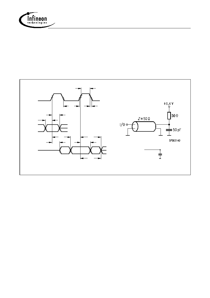
SPT03404
CLOCK
2.4 V
0.4 V
INPUT
HOLD
t
SETUP
t
t
T
OUTPUT
1.4 V
t
LZ
AC
t
t
AC
OH
t
HZ
t
1.4 V
CL
t
CH
t
50 pF
I/O
Measurement conditions for
t
AC
and
t
OH
HYB 39S64400/800/160BT(L)
64-MBit Synchronous DRAM
Data Book
20
12.99
Package Outlines
GPX09039
22.22
±0.13
1)
1
27
54
28
0.35
+0.1
-0.05
0.1
1
0.1
10.16
±0.13
±0.2
11.76
±0.1
0.5
Does not include plastic or metal protrusion of 0.15 max per side
1)
54x
±0.05
±0.05
0.15
-0.03
+0.06
15∞
±5∞
15∞
±5∞
6 max
2.5 max
2)
3)
Does not include plastic protrusion of 0.25 max per side
2)
Does not include dambar protrusion of 0.13 max per side
3)
Index Marking
0.8
20.8
26x 0.8 =
0.2
M
54x
Plastic Package, P-TSOPII-54
(400 mil, 0.8 mm lead pitch)
Thin Small Outline Package, SMD
Sorts of Packing
Package outlines for tubes, trays etc. are contained in our
Data Book "Package Information".
Dimensions in mm
SMD = Surface Mounted Device

HYB39S64400/800/160BT(L)
64MBit Synchronous DRAM
Semiconductor Group
20
Timing Diagrams
1. Bank Activate Command Cycle
2. Burst Read Operation
3. Read Interrupted by a Read
4. Read to Write Interval
4.1 Read to Write Interval
4.2 Minimum Read to Write Interval
4.3 Non-Minimum Read to Write Interval
5. Burst Write Operation
6. Write and Read Interrupt
6.1 Write Interrupted by a Write
6.2 Write Interrupted by Read
7. Burst Write & Read with Auto-Precharge
7.1 Burst Write with Auto-Precharge
7.2 Burst Read with Auto-Precharge
8. Burst Termination
8.1 Termination of a full Page Burst Write Operation
8.2 Termination of a full Page Burst Write Operation
9. AC- Parameters
9.1 AC Parameters for a Write Timing
9.2 AC Parameters for a Read Timing
10. Mode Register Set
11. Power on Sequence and Auto Refresh (CBR)
12. Clock Suspension (using CKE)
12. 1 Clock Suspension During Burst Read CAS Latency = 2
12. 2 Clock Suspension During Burst Read CAS Latency = 3
12. 3 Clock Suspension During Burst Write CAS Latency = 2
12. 4 Clock Suspension During Burst Write CAS Latency = 3
13. Power Down Mode and Clock Suspend
14. Self Refresh ( Entry and Exit )
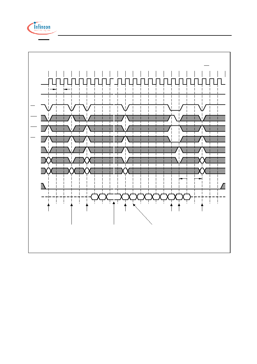
15. Auto Refresh ( CBR )
16. Random Column Read ( Page within same Bank)
16.1 CAS Latency = 2
16.2 CAS Latency = 3
17. Random Column Write ( Page within same Bank)
17.1 CAS Latency = 2
17.2 CAS Latency = 3

HYB39S64400/800/160BT(L)
64MBit Synchronous DRAM
Semiconductor Group
21
Timing Diagrams
(cont'd)
18. Random Row Read ( Interleaving Banks) with Precharge
18.1 CAS Latency = 2
18.2 CAS Latency = 3
19. Random Row Write ( Interleaving Banks) with Precharge
19.1 CAS Latency = 2
19.2 CAS Latency = 3
20. Full Page Read Cycle
20.1 CAS Latency = 2
20.2 CAS Latency = 3
21. Full Page Write Cycle
21.1 CAS Latency = 2
21.2 CAS Latency = 3
22. Precharge Termination of a Burst
HYB39S64400/800/160BT(L)
64MBit Synchronous DRAM
Semiconductor Group
22
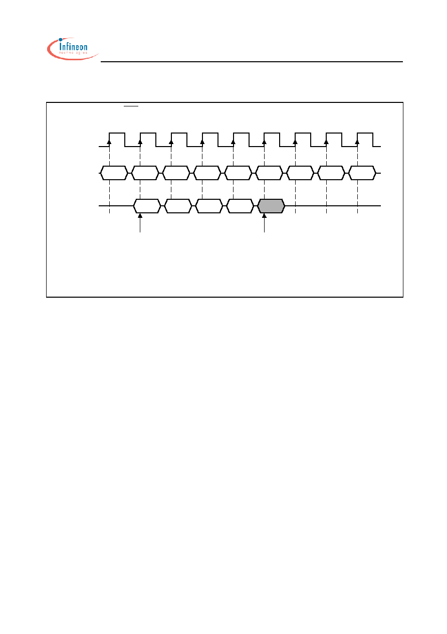
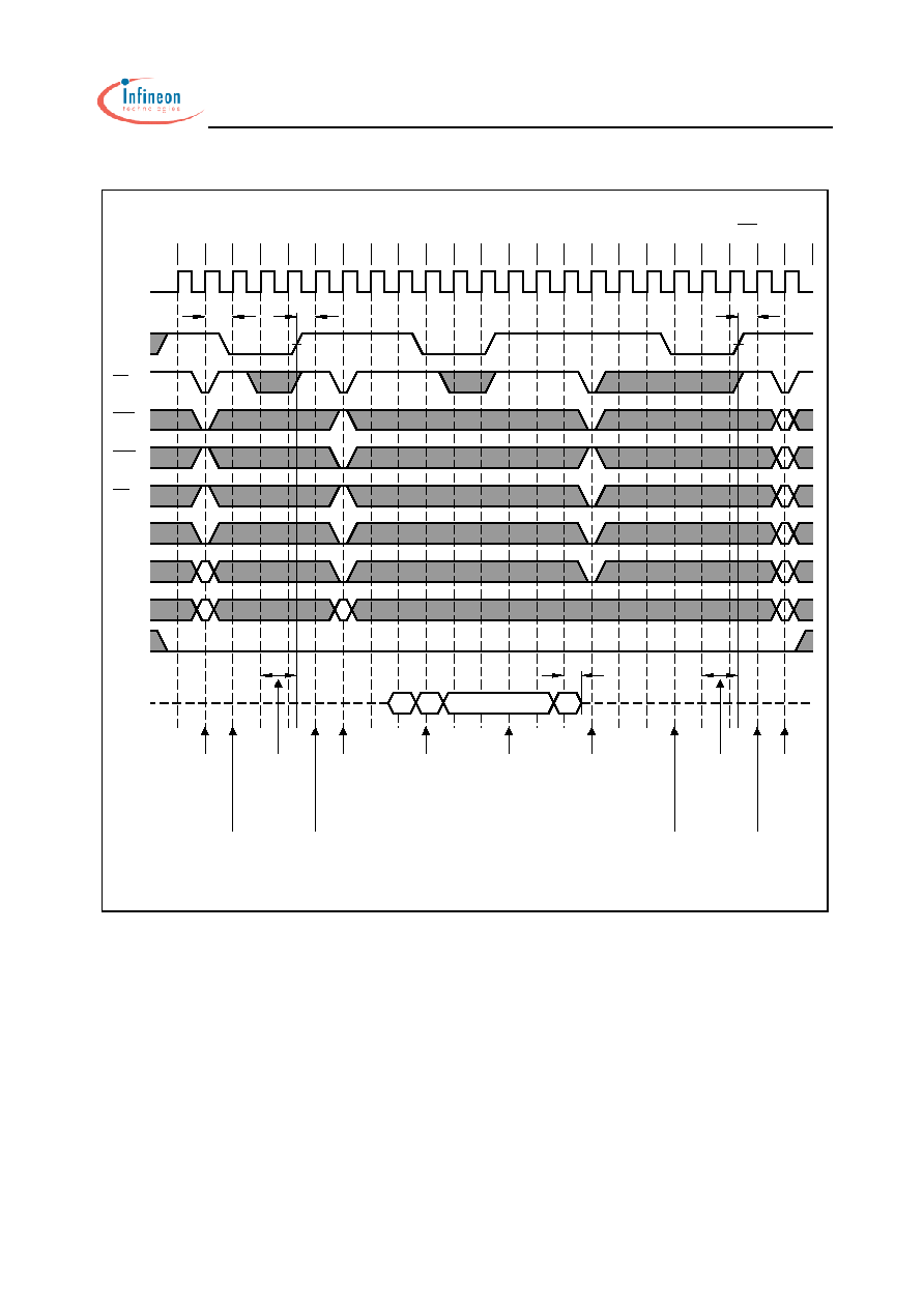
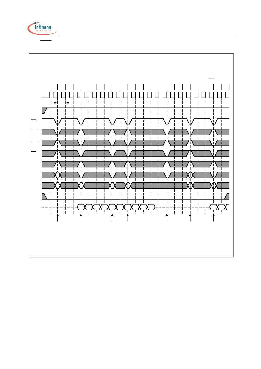
1. Bank Activate Command Cycle
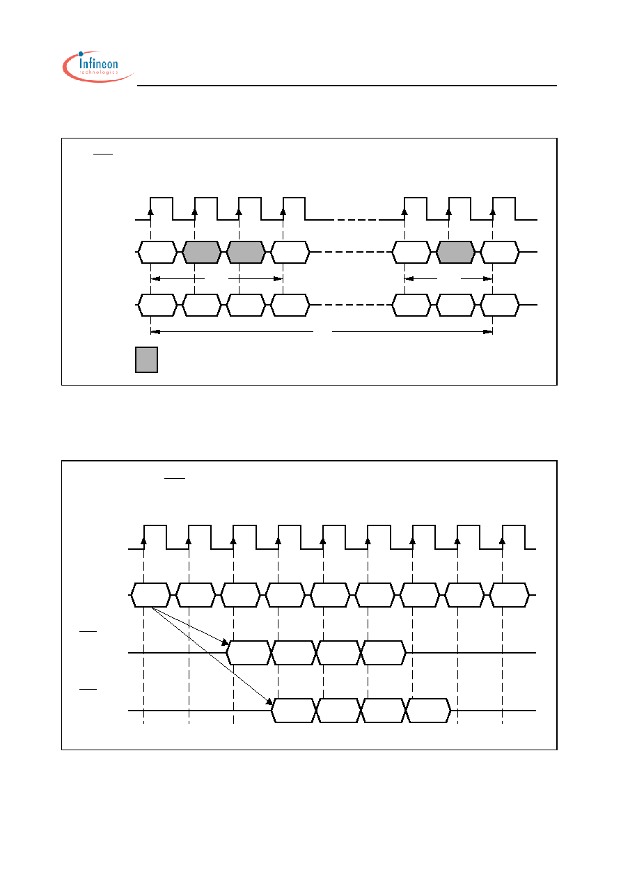
2. Burst Read Operation
RC
"H" or "L"
t
T0
(CAS latency = 3)
Bank B
Row Addr.
Activate
Bank B
Address
Command
CLK
T
NOP
NOP
RCD
t
T1
Col. Addr.
Bank B
with Auto
Precharge
Write B
T
SPT03784
Bank B
Row Addr.
Activate
Bank B
Row Addr.
Bank A
Activate
Bank A
T
NOP
RRD
t
T
T
SPT03712
CLK
Read A
NOP
T0
T1
T2
T3
T4
T5
T6
T7
T8
Command
NOP
NOP
NOP
NOP
NOP
NOP
NOP
DOUT A3
CK2
latency = 2
t
, DQ's
DOUT A1
DOUT A0
DOUT A2
DOUT A2
CK3
latency = 3
t
, DQ's
DOUT A0 DOUT A1
DOUT A3
(Burst Length = 4, CAS latency = 2, 3)
CAS
CAS

HYB39S64400/800/160BT(L)
64MBit Synchronous DRAM
Semiconductor Group
23
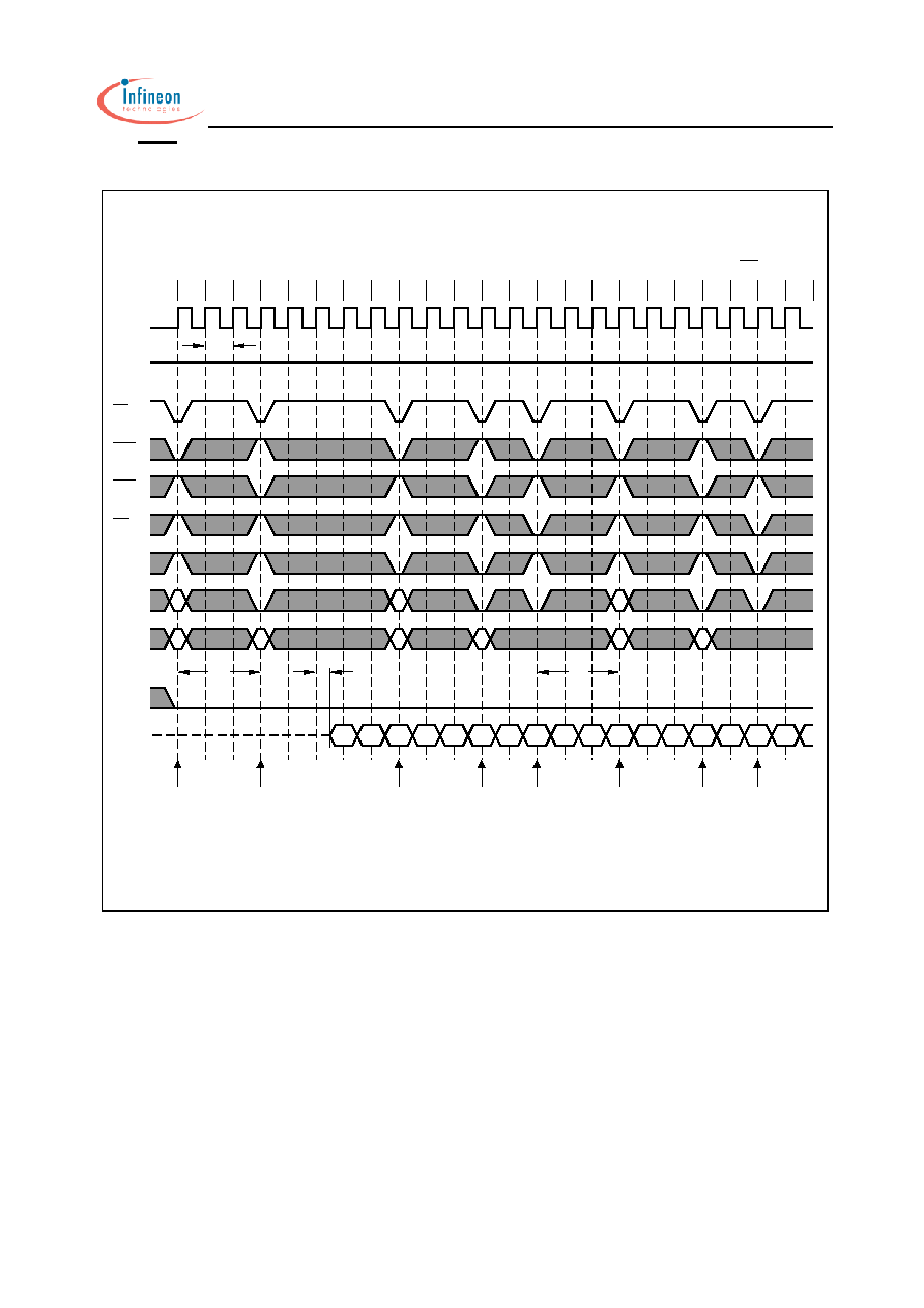
3. Read Interrupted by a Read
4. Read to Write Intrerval
4.1 Read to Write Interval
SPT03713
CLK
Read A
T0
T1
T2
T3
T4
T5
T6
T7
T8
Command
DOUT A0 DOUT B0 DOUT B1 DOUT B2
NOP
NOP
NOP
NOP
NOP
NOP
NOP
latency = 2
, DQ's
CK2
t
CK3
latency = 3
t
, DQ's
(Burst Length = 4, CAS latency = 2, 3)
CAS
CAS
Read B
DOUT B3
DOUT B1
DOUT A0 DOUT B0
DOUT B3
DOUT B2
Commands = 4 + 1 = 5 cycles
Minimum delay between the Read and Write
DOUT A0
DQ's
(Burst Length = 4, CAS latency = 3)
DQMx
Command
CLK
NOP
Read A
T0
T1
NOP
NOP
T2
T3
the Write Command
Must be Hi-Z before
DIN B0
DIN B1
SPT03787
DIN B2
DQW
NOP
DQZ
t
NOP
t
T4
T5
Write B
NOP
T6
T7
NOP
T8
"H" or "L"
Write latency
of DQMx
HYB39S64400/800/160BT(L)
64MBit Synchronous DRAM
Semiconductor Group
24
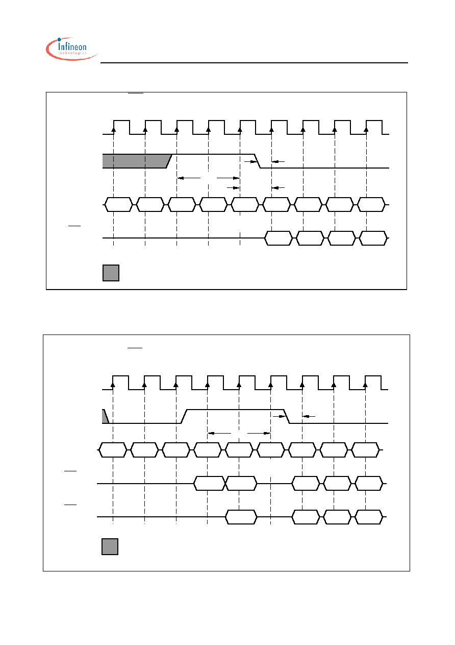
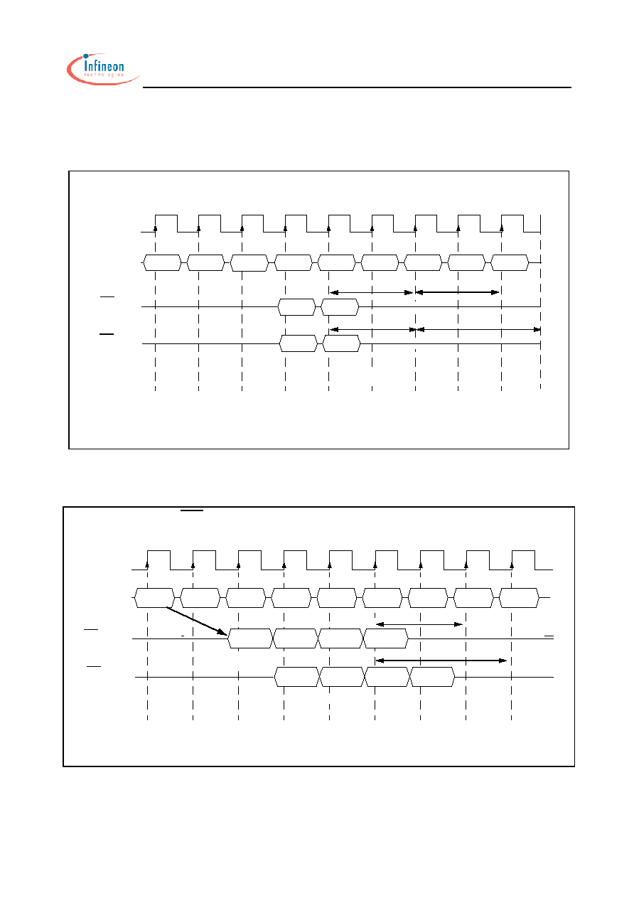
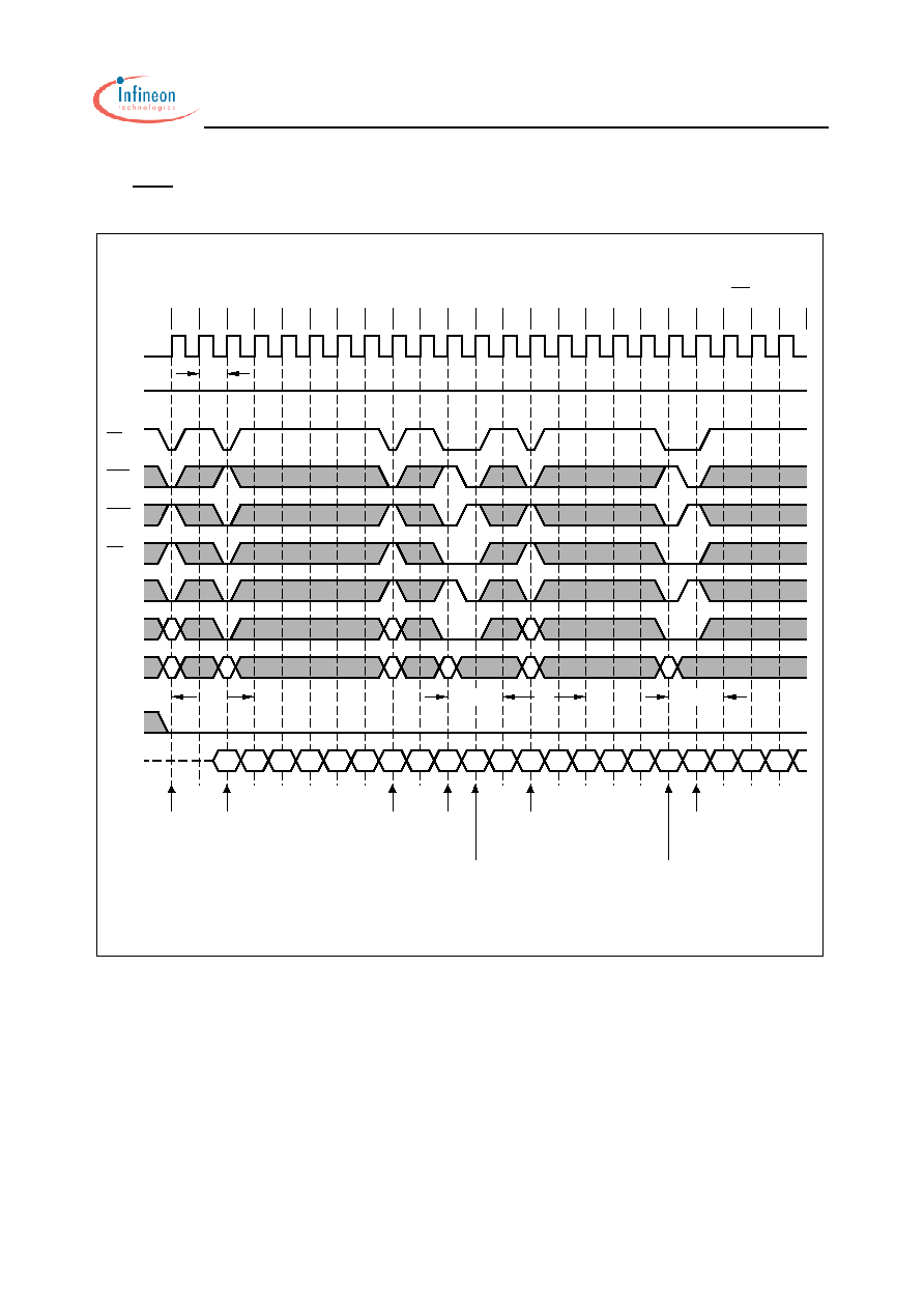
4 2. Minimum Read to Write Interval
4. 3. Non-Minimum Read to Write Interval
the Write Command
Must be Hi-Z before
Activate
CAS
CK2
latency = 2
t
, DQ's
(Burst Length = 4, CAS latency = 2)
CLK
DQM
Command
NOP
T0
T1
Bank A
NOP
DQZ
t
T2
T3
DIN A0
DIN A1
DIN A2
SPT03939
DIN A3
1 Clk Interval
Read A
Write A
T4
T5
NOP
NOP
T6
T7
NOP
T8
"H" or "L"
t
DQW
NOP
CAS
latency = 3
CK3
CAS
CK2
latency = 2
t
t
, DQ's
, DQ's
DOUT A0
(Burst Length = 4, CAS latency = 2, 3)
CLK
DQM
Command
NOP
Read A
T0
T1
NOP
NOP
T2
T3
the Write Command
Must be Hi-Z before
DOUT A0
DOUT A1
DIN B0
DIN B0
DIN B1
DIN B1
SPT03940
DIN B2
DIN B2
Read A
DQZ
t
NOP
T4
T5
Write B
NOP
T6
T7
NOP
T8
"H" or "L"
t
DQW
HYB39S64400/800/160BT(L)
64MBit Synchronous DRAM
Semiconductor Group
25
5. Burst Write Operation
Extra data is ignored after
termination of a Burst.
DIN A3
T4
are registered on the same clock edge.
The first data element and the Write
NOP
(Burst Length = 4, CAS latency = 2, 3)
T0
Command
DQ's
CLK
DIN A1
T2
NOP
DIN A0
Write A
T1
DIN A2
NOP
T3
SPT03790
T6
NOP
NOP
T5
NOP
NOP
T7
NOP
T8
don't care
HYB39S64400/800/160BT(L)
64MBit Synchronous DRAM
Semiconductor Group
26
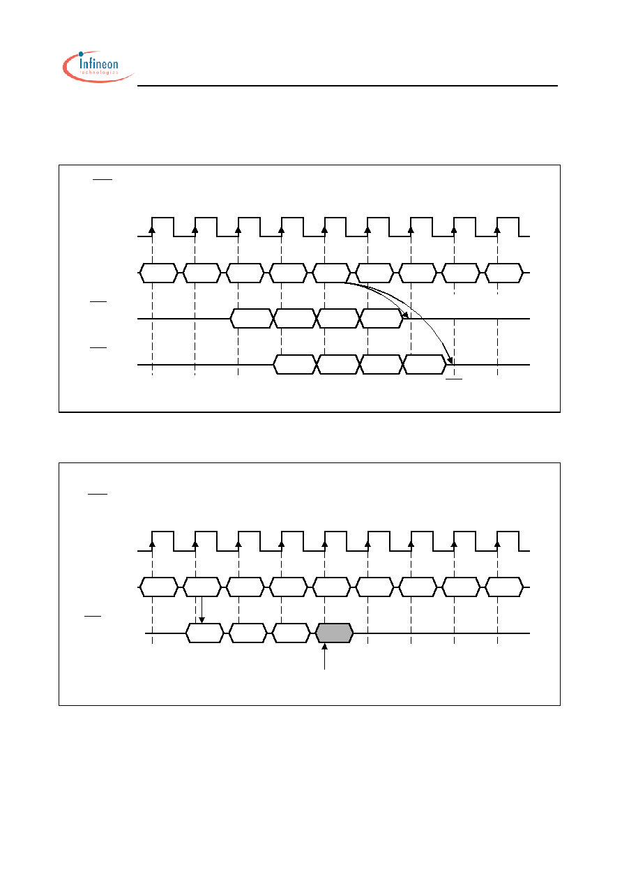
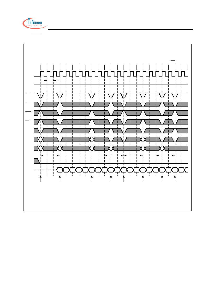
6. Write and Read Interrupt
6.1 Write Interrupted by a Write
6.2 Write Interrupted by a Read
1 Clk Interval
SPT03791
CLK
T0
T1
T2
T3
T4
T5
T6
T7
T8
Command
NOP
NOP
NOP
NOP
NOP
NOP
DQ's
(Burst Length = 4, CAS latency = 2, 3)
NOP
Write A
DIN A0
DIN B0
DIN B1
DIN B2
DIN B3
Write B
1 Clk Interval
T5
NOP
DOUT B1
DOUT B0
Input data for the Write is ignored.
, DQ's
latency = 3
CK3
CAS
t
don't care
DIN A0
don't care
(Burst Length = 4, CAS latency = 2, 3)
CLK
, DQ's
Command
latency = 2
CK2
CAS
t
NOP
T0
DIN A0
Write A
don't care
Read B
T1
T2
DOUT B0
NOP
NOP
T4
T3
SPT03719
appears on the outputs to avoid data contention.
DOUT B2
Input data must be removed from the DQ's
at least one clock cycle before the Read data
DOUT B1
DOUT B3
NOP
DOUT B3
NOP
DOUT B2
T6
T7
NOP
T8
HYB39S64400/800/160BT(L)
64MBit Synchronous DRAM
Semiconductor Group
27
7. Burst Write and Read with Auto Precharge
7.1 Burst Write with Auto-Precharge
7.2 Burst Read with Auto-Precharge
COMMAND
NOP
NOP
NOP
WRITE A
Auto-Precharge
CLK
T0
T2
T1
T3
T4
T5
T6
T7
T8
NOP
BANK A
ACTIVE
NOP
NOP
DIN A0
DIN A1
DIN A0
DIN A1
*
*
DQ's
CAS latency = 2
DQ's
CAS latency = 3
Begin Autoprecharge
Bank can be reactivated after trp
*
t
WR
t
WR
t
RP
t
RP
NOP
COMMAND
READ A
NOP
NOP
NOP
NOP
NOP
NOP
NOP
t
CK2,
DQ's
CAS latency = 2
t
CK3,
DQ's
CAS latency = 3
NOP
CLK
T0
T2
T1
T3
T4
T5
T6
T7
T8
DOUT A0
DOUT A1
DOUT A2
DOUT A3
DOUT A0
DOUT A1
DOUT A2
DOUT A3
with AP
Begin Autoprecharge
Bank can be reactivated after trp
*
*
*
t
RP
t
RP
(Burst Length = 4, CAS latency = 2,3)
HYB39S64400/800/160BT(L)
64MBit Synchronous DRAM
Semiconductor Group
28
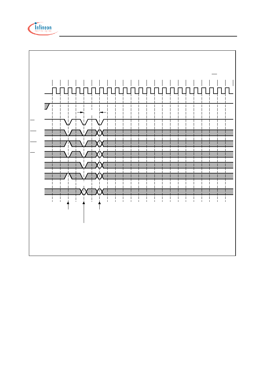
8. Burst Termination
8.1 Termination of a Full Page Burst Read Operation
8.2 Termination of a Full Page Burst Write Operation
SPT03722
CLK
NOP
T0
T1
T2
T3
T4
T5
T6
T7
T8
Command
DOUT A0 DOUT A1 DOUT A2 DOUT A3
NOP
NOP
Burst
NOP
NOP
NOP
NOP
latency = 2
, DQ's
CK2
t
DOUT A3
CK3
latency = 3
t
, DQ's
DOUT A1
DOUT A0
DOUT A2
(CAS latency = 2, 3)
CAS
CAS
Read A
The burst ends after a delay equal to the CAS latency.
Terminate
Input data for the Write is masked.
T4
latency = 2, 3
DQ's
NOP
(CAS latency = 2, 3)
T0
Command
CAS
CLK
DIN A1
T2
NOP
DIN A0
Write A
T1
DIN A2
NOP
T3
SPT03419
T6
Burst
Terminate
NOP
T5
NOP
NOP
T7
NOP
T8
don't care
HYB39S64400/800/160BT(L)
64MBit Synchronous DRAM
Semiconductor Group
29
9. AC Parameters
9.1 AC Parameters for a Write Timing
Auto Precharge
Bank B
Command
Write with
Activate
Write with
Activate
Bank A
Command
Auto Precharge
Bank A
Command
Command
Bank B
Addr.
AP
DQM
DQ
BS
Hi-Z
RCD
t
Ax2
Ax1
Ax0
Ax3
RC
t
RAx
RAx
t
AS
t
AH
RBx
RBx
CAx
Activate
Precharge
Activate
Write
Command
Command
Bank A
Bank A
Command
Bank A
Bank A
Command
SPT03910
Bx2
Bx1
Bx0
Bx3
DS
t
t
DH
Ay2
Ay1
Ay0
Ay3
t
WR
RAy
RAy
CBx
RAy
RP
t
RAz
RAz
T8
Precharge
Begin Auto
Bank A
CLK
WE
CAS
RAS
CS
CKE
CK2
t
CS
t
CH
CKS
t
CH
t
t
CL
t
T3
T0
T2
T1
T4
T5
T7
T6
Bank B
Precharge
Begin Auto
t
CKH
T18
Burst Length = 4, CAS Latency = 2
T13
T9
T10
T12
T11
T14 T15
T17
T16
T19 T20
T22
T21
RBy
RBy
RRD
t
Activate
Bank B
Command
HYB39S64400/800/160BT(L)
64MBit Synchronous DRAM
Semiconductor Group
30
9.2 AC Parameters for a Read Timing
AC2
Hi-Z
DQ
Activate
Command
Bank A
Read with
Bank A
Command
Auto Precharge
DQM
Addr.
AP
t
RCD
t
LZ
t
t
AS
RAx
RAx
t
AH
CAx
RRD
t
Command
Bank B
Read with
Auto Precharge
Activate
Bank B
Command
Ax1
Ax0
Bx0
Activate
SPT03911
Command
Bank A
Bx1
t
AC2
OH
t
HZ
t
t
RAS
RC
t
RBx
RBx
RBx
HZ
t
RAy
RAy
T5
t
t
BS
WE
CAS
RAS
t
CS
CKE
CKS
t
CH
t
t
CS
CH
CL
CK2
CLK
T0
T1
T2
T3
T4
Precharge
Bank A
Begin Auto
Precharge
Bank B
Begin Auto
t
CKH
Burst Length = 2, CAS Latency = 2
T6
T7
T8
T10
T9
T11
T13
T12
RP
t
Precharge
Bank A
Command
HYB39S64400/800/160BT(L)
64MBit Synchronous DRAM
Semiconductor Group
31
10. Mode Register Set
Set Command
Mode Register
All Banks
Precharge
Command
Any
Command
Address Key
T0
T1
T2
T8
RSC
t
T4
T3
T5
T6
T7
T11
T9
T10
T12 T13
SPT03912
T19
T16
T15
T14
T17 T18
CAS Latency = 2
T20 T21 T22
BS0, BS1
A0-A9
A10, A11
CS
WE
CAS
RAS
CKE
CLK
HYB39S64400/800/160BT(L)
64MBit Synchronous DRAM
Semiconductor Group
32
11. Power on Sequence and Auto Refresh (CBR)
Inputs must be
200
stable for
µ
s
DQM
AP
DQ
Addr.
BS
RP
Command
All Banks
Precharge
Hi-Z
~ ~
t
1st Auto Refresh
Command
~ ~
~ ~
~ ~
~ ~
~ ~
~ ~
~ ~
SPT03913
Mode Register
Set Command
Address Key
8th Auto Refresh
Command
~~
t
RC
~~
~~
~~
~ ~
~ ~
~~
~~
Command
Any
Minimum of 8 Refresh Cycles are required
T8
WE
CAS
RAS
CS
CKE
CLK
required
~~
~ ~
~ ~
~ ~
~ ~
~ ~
~ ~
T3
is
~~
~ ~
Level
High
T0
T2
T1
T5
T4
T7
T6
T18
2 Clock min.
~ ~
~ ~
~ ~
~ ~
~ ~
~ ~
~~
T13
~~
~~
T10
T9
T12
T11
T14 T15
T17
T16
T20
T19
T22
T21
HYB39S64400/800/160BT(L)
64MBit Synchronous DRAM
Semiconductor Group
33
12. Clock Suspension ( Using CKE)
12.1 Clock Suspension During Burst Read CAS Latency = 2
Command
Bank A
DQM
Addr.
DQ
AP
BS
Read
Command
Bank A
Activate
Hi-Z
Suspend
1 Cycle
Clock
Ax0
CSL
t
Ax1
CAx
RAx
RAx
SPT03914
t
Suspend
3 Cycles
Suspend
2 Cycles
Clock
Ax2
CSL
t
Clock
Ax3
HZ
T7
WE
CAS
RAS
CS
CKE
CLK
CK2
t
T0
T1
T2
T3
T4
T6
T5
T16
T8
T9
T10 T11
T14
T12 T13
T15
Burst Length = 4, CAS Latency = 2
T18
T17
T19 T20 T21 T22
CSL
t
HYB39S64400/800/160BT(L)
64MBit Synchronous DRAM
Semiconductor Group
34
12.2 Clock Suspension During Burst Read CAS Latency = 3
CSL
DQM
Addr.
DQ
AP
BS
Bank A
Activate
Command
Hi-Z
Command
Bank A
Read
Ax0
t
RAx
RAx
CAx
HZ
t
t
Suspend
1 Cycle
Clock
Suspend
2 Cycles
Clock
CSL
Ax1
Ax2
Clock
Suspend
3 Cycles
t
CSL
Ax3
SPT03915
T7
WE
CAS
RAS
CS
CKE
CLK
CK3
t
T0
T1
T2
T3
T4
T6
T5
T16
T8
T9
T10 T11
T14
T12 T13
T15
Burst Length = 4, CAS Latency = 3
T18
T17
T19 T20 T21 T22
HYB39S64400/800/160BT(L)
64MBit Synchronous DRAM
Semiconductor Group
35
12.3 Clock Suspension During Burst Write CAS Latency = 2
Bank A
DQM
Addr.
DQ
AP
BS
DAx0
Command
Write
Activate
Command
Bank A
Hi-Z
Clock
Clock
1 Cycle
Suspend
Suspend
2 Cycles
DAx1
CAx
RAx
RAx
DAx3
Clock
Suspend
3 Cycles
DAx2
SPT03916
T7
WE
CAS
RAS
CS
CKE
CLK
CK2
t
T0
T1
T2
T3
T4
T6
T5
T16
T8
T9
T10 T11
T14
T12 T13
T15
Burst Length = 4, CAS Latency = 2
T18
T17
T19 T20 T21 T22
HYB39S64400/800/160BT(L)
64MBit Synchronous DRAM
Semiconductor Group
36
12.4 Clock Suspension During Burst Write CAS Latency = 3
Clock
Suspend
2 Cycles
Bank A
DQMx
Addr.
DQ
A8/AP
BA
Activate
Command
Bank A
Hi-Z
Clock
1 Cycle
Suspend
Command
Write
DAx0
DAx1
RAx
RAx
CAx
Clock
Suspend
3 Cycles
DAx2
DAx3
SPT03917
T7
WE
CAS
RAS
CS
CKE
CLK
CK3
t
T0
T1
T2
T3
T4
T6
T5
T16
T8
T9
T10 T11
T14
T12 T13
T15
Burst Length = 4, CAS Latency = 3
T18
T17
T19 T20 T21 T22
HYB39S64400/800/160BT(L)
64MBit Synchronous DRAM
Semiconductor Group
37
13. Power Down Mode and Clock Suspend
BS
Clock Suspend
Clock Suspend
Mode Entry
Mode Exit
Addr.
DQM
DQ
AP
Standby
Active
Activate
Bank A
Command
Hi-Z
Read
Command
Bank A
RAx
RAx
CAx
Power Down
Power Down
Mode Exit
Mode Entry
SPT03918
End
Clock Mask
Clock Mask
Start
Ax0 Ax1
Ax2
Precharge
Command
Bank A
Ax3
t
HZ
Precharge
Standby
Any
Command
T7
CAS
WE
RAS
CS
CKE
CLK
CK2
t
T0
T1
T2
CKS
t
T3
T4
T6
T5
T16
T8
T9
T10 T11
T14
T12 T13
T15
Burst Length = 4, CAS Latency = 2
CKS
t
T18
T17
T19 T20 T21 T22
HYB39S64400/800/160BT(L)
64MBit Synchronous DRAM
Semiconductor Group
38
14. Self Refresh (Entry and Exit)
BS
t
Self Refresh Exit
Command issued
Addr.
DQM
DQ
AP
Entry
Self Refresh
must be idle
All Banks
Hi-Z
~ ~
~ ~
~ ~
~ ~
~ ~
~ ~
~ ~
SPT03919
Exit Command
Begin Self Refresh
SREX
t
RC
Self Refresh
Command
Exit
Any
T7
CS
CAS
WE
RAS
CKE
CLK
~ ~
~ ~
~ ~
~ ~
~ ~
~ ~
~ ~
~ ~
t
CKS
T0
T1
T2
~ ~
~ ~
T3
T4
~~
~~
T6
T5
T16
CKS
t
T8
T9
T10 T11
T14
T12 T13
T15
T18
T17
T19 T20 T21 T22

HYB39S64400/800/160BT(L)
64MBit Synchronous DRAM
Semiconductor Group
39
15. Auto Refresh (CBR)
(Minimum Interval)
Addr.
DQM
DQ
AP
BS
Auto Refresh
Command
All Banks
Precharge
Command
Hi-Z
t
RP
t
RC
SPT03920
Command
Command
Auto Refresh
Command
Bank A
Activate
RC
t
RAx
RAx
Ax2
Bank A
Read
Ax0 Ax1
Ax3
CAx
T7
WE
CAS
RAS
CS
CKE
CLK
CK2
t
T0
T1
T2
T3
T4
T6
T5
T16
T8
T9
T10 T11
T14
T12 T13
T15
Burst Length = 4, CAS Latency = 2
T18
T17
T19 T20 T21 T22
HYB39S64400/800/160BT(L)
64MBit Synchronous DRAM
Semiconductor Group
40
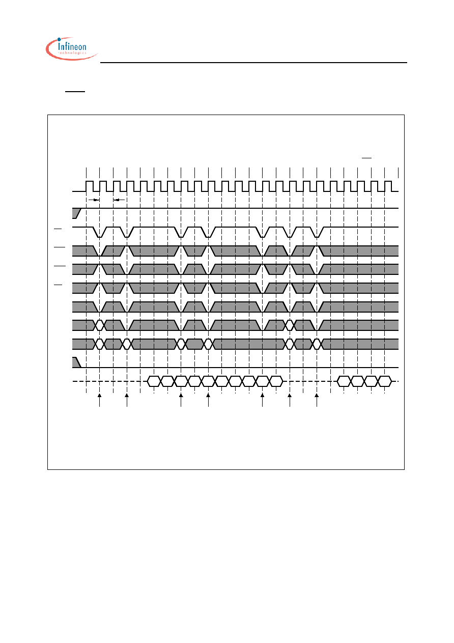
16. Random Column Read (Page within same Bank)
16.1 CAS Latency = 2
Ay1
Addr.
BS
DQ
DQM
AP
Activate
Command
Z
Hi
Bank A
RAw
RAw
Command
Read
Command
Bank A
Read
Bank A
Aw0 Aw1
CAw
CAx
Read
Bank A
Command
Aw3
Aw2
Ax0 Ax1 Ay0
CAy
CS
WE
CAS
RAS
CKE
CLK
T0
CK2
t
T1
T2
T8
T4
T3
T5
T6
T7
T11
T9
T10
T12 T13
Precharge
Command
Bank A
Ay2 Ay3
Activate
Command
Bank A
RAz
RAz
SPT03921
Read
Bank A
Command
CAz
Burst Length = 4, CAS Latency = 2
T19
T16
T15
T14
T17 T18
T20 T21 T22
Az3
Az0 Az1 Az2

HYB39S64400/800/160BT(L)
64MBit Synchronous DRAM
Semiconductor Group
41
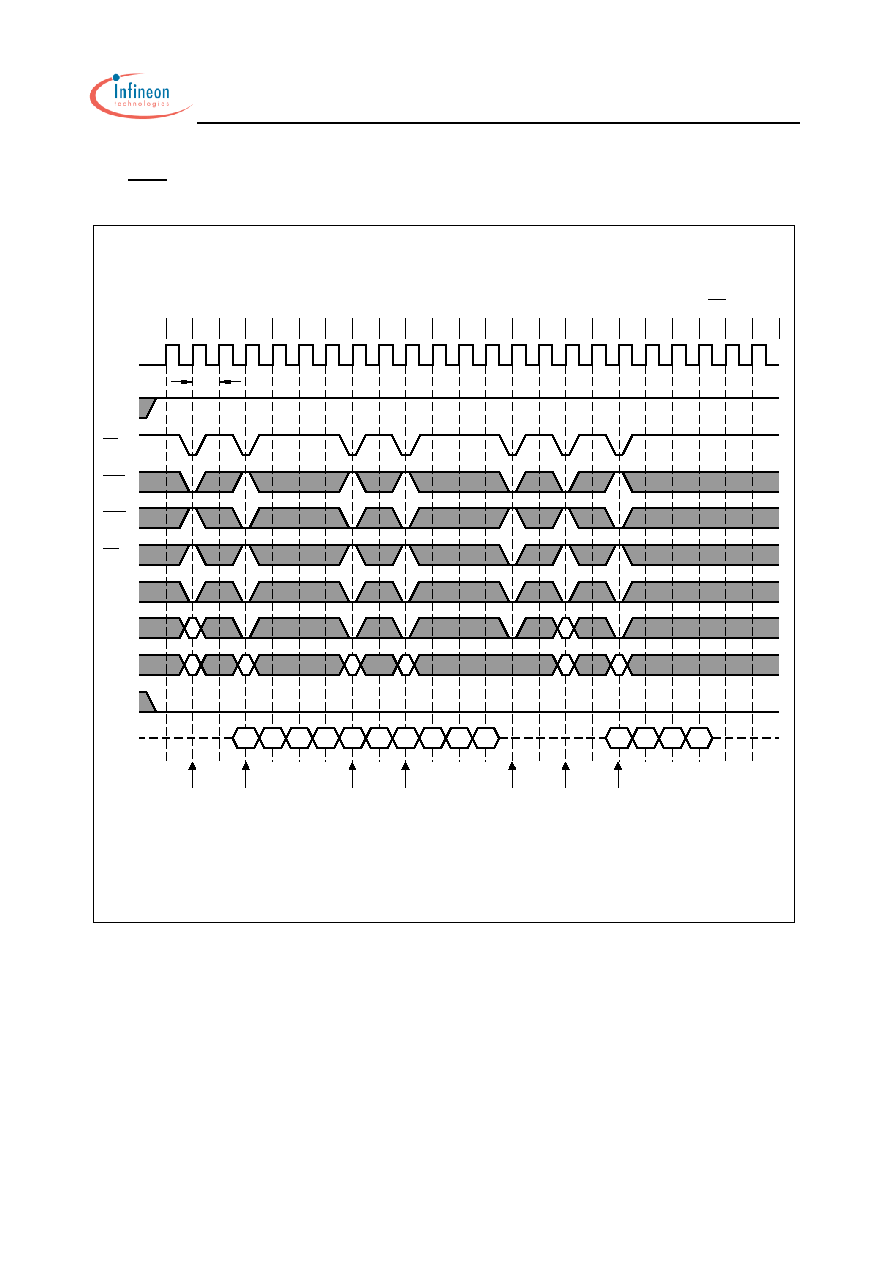
16.2 CAS Latency = 3
Ay3
CAw
Addr.
BS
DQ
DQM
AP
Z
Hi
Bank A
Activate
Command
Read
Command
Bank A
RAw
RAw
Bank A
Command
Aw1
Aw0
Read
Bank A
Command
Aw2 Aw3
CAx
Read
Ax1
Ax0
Ay0
Precharge
Command
Bank A
Ay1 Ay2
CAy
CS
WE
CAS
RAS
CKE
CLK
T0
CK3
t
T1
T2
T8
T4
T3
T5
T6
T7
T11
T9
T10
T12 T13
Bank A
Read
Command
Activate
Command
Bank A
RAz
RAz
CAz
SPT03922
Burst Length = 4, CAS Latency = 3
T19
T16
T15
T14
T17 T18
T20 T21 T22
HYB39S64400/800/160BT(L)
64MBit Synchronous DRAM
Semiconductor Group
42
17. Random Column write (Page within same Bank)
17.1 CAS Latency = 2
DBy1
Addr.
BS
DQ
DQM
AP
Activate
Command
Z
Hi
Bank A
RAw
RAw
Command
Write
Command
Bank B
Write
Bank B
DBw0 DBw1
CAw
CAx
Write
Bank B
Command
DBw3
DBw2
DBx0 DBx1 DBy0
CAy
CS
WE
CAS
RAS
CKE
CLK
T0
CK2
t
T1
T2
T8
T4
T3
T5
T6
T7
T11
T9
T10
T12 T13
Precharge
Command
Bank B
DBy2 DBy3
Activate
Command
Bank B
RAz
RAz
SPT03923
Read
Bank B
Command
CAz
Burst Length = 4, CAS Latency = 2
T19
T16
T15
T14
T17 T18
T20 T21 T22
DBz1
DBz0
DBz2 DBz3
HYB39S64400/800/160BT(L)
64MBit Synchronous DRAM
Semiconductor Group
43
17.2. CAS Latency = 3
Command
Write
Bank B
CBz
DBw0
Addr.
BS
DQ
DQM
AP
Bank B
Activate
Command
Z
Hi
RBz
RBz
Command
Bank B
DBw3
DBw1 DBw2
Write
Bank B
Command
DBx0 DBx1
CBx
Write
DBy1
DBy0
DBy2
Precharge
Command
Bank B
DBy3
CBy
CS
WE
CAS
RAS
CKE
CLK
T0
CK3
t
T1
T2
T8
T4
T3
T5
T6
T7
T11
T9
T10
T12 T13
Command
Bank B
DBz0
Activate
Command
Bank B
Write
DBz1
RBz
RBz
CBz
SPT03924
Burst Length = 4, CAS Latency = 3
T19
T16
T15
T14
T17 T18
T20 T21 T22

HYB39S64400/800/160BT(L)
64MBit Synchronous DRAM
Semiconductor Group
44
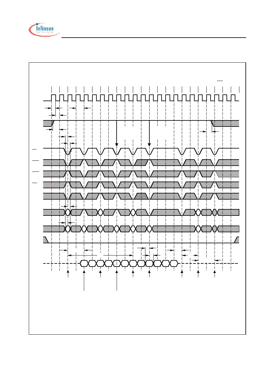
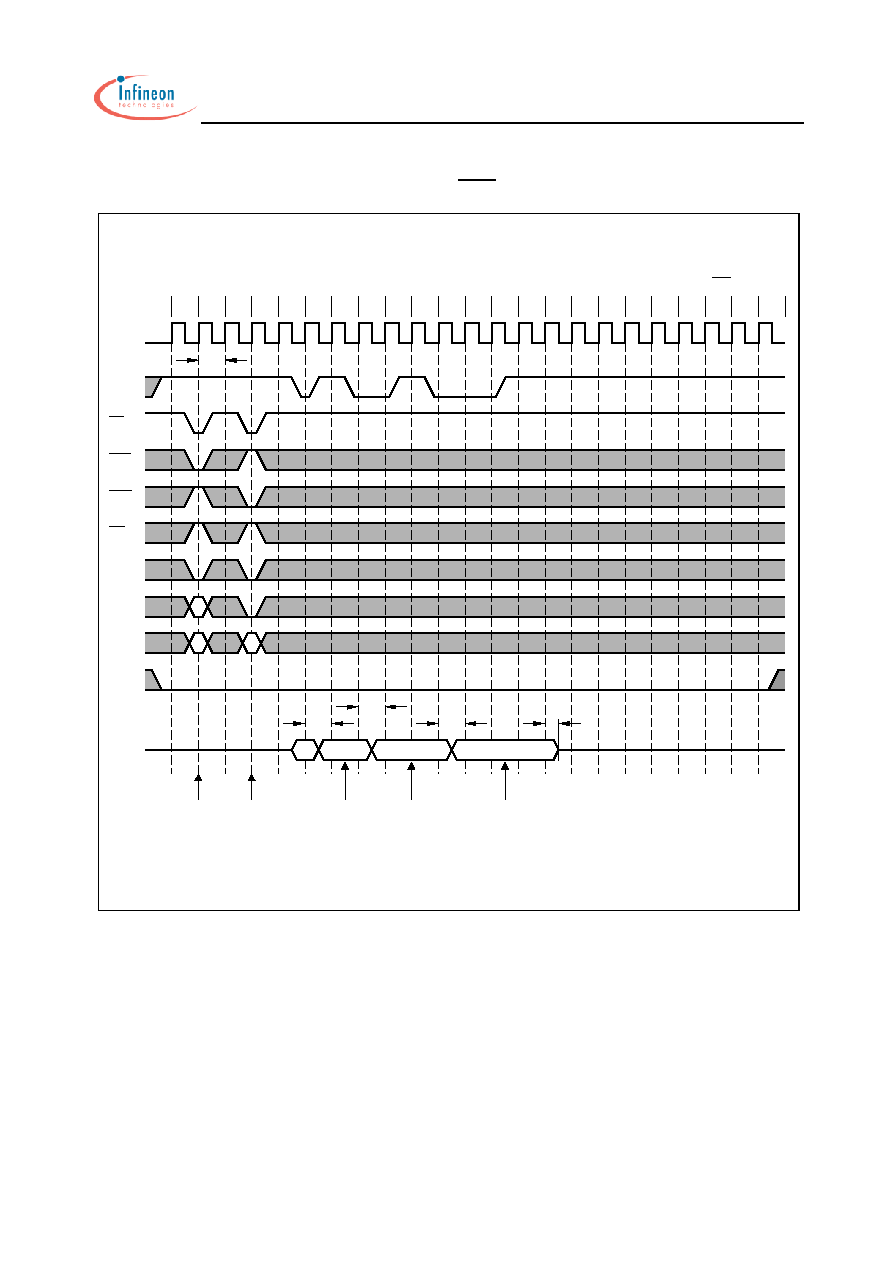
18. Random Row Read (Interleaving Banks) with Precharge
18.1 CAS Latency = 2
Ax2
t
BS
Addr.
DQ
DQM
AP
Bank B
Activate
Command
Hi-Z
Command
Read
Bank B
RBx
RBx
RCD
t
CBx
Read
Activate
Bank A
Command
Command
Bank B
Command
Bx2
Bx0
AC2
Bx1
Bank A
Activate
Bx3 Bx4
RAx
RAx
Command
Precharge
Bank B
Bx6
Bx5
Bx7 Ax0 Ax1
CAx
RP
t
RBy
RBy
CS
WE
CAS
RAS
CKE
CLK
T0
High
t
CK2
T1
T2
T8
T4
T3
T5
T6
T7
T11
T9
T10
T12 T13
SPT03925
Bank B
Command
Ax5
Ax3 Ax4
Read
Ax6 Ax7
CBy
By1
By0
Burst Length = 8, CAS Latency = 2
T19
T16
T15
T14
T17 T18
T20 T21 T22
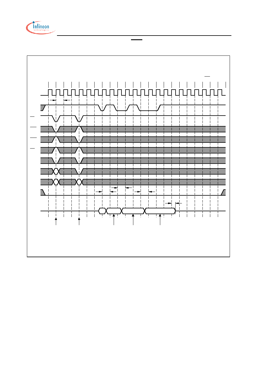
HYB39S64400/800/160BT(L)
64MBit Synchronous DRAM
Semiconductor Group
45
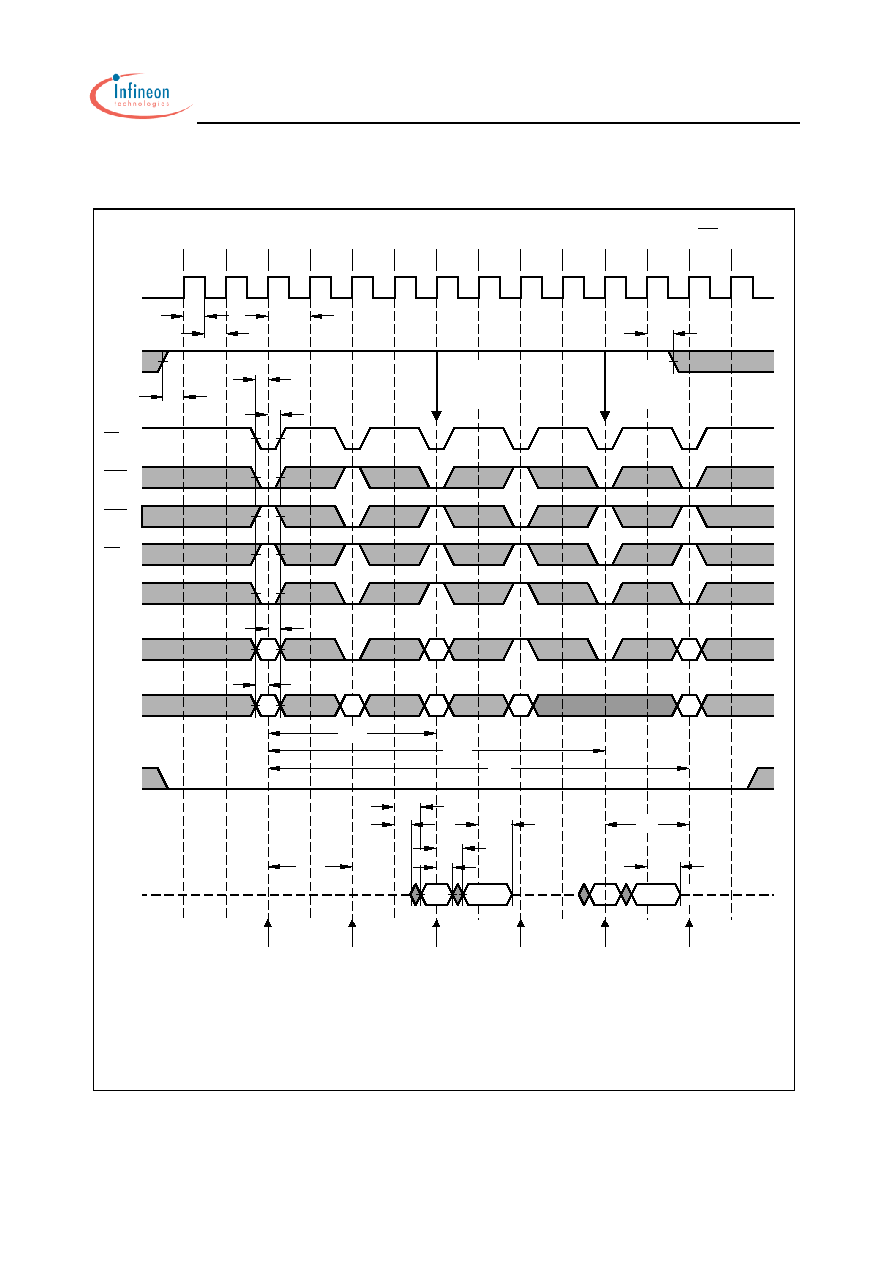
18.2 CAS Latency = 3
Activate
Command
Bank A
Addr.
DQM
DQ
AP
BS
Read
Bank B
Command
Command
Bank B
Activate
Hi-Z
Bx1
Bx0
CBx
RBx
RCD
t
RBx
t
AC3
Activate
Command
Bank B
Bx6
Bank A
Command
Read
Bx4
Bx3
Bx2
Bx5
Bank B
Precharge
Command
Ax0
Bx7
Ax2
Ax1
RAx
CAx
RAx
RP
t
RBy
RBy
Precharge
Bank A
Command
Ax7
Read
Bank B
Command
Ax5
Ax4
Ax3
Ax6
SPT03926
By0
CBy
T7
WE
CAS
RAS
CS
CKE
CLK
High
CK3
t
T0
T1
T2
T3
T4
T6
T5
T16
T8
T9
T10 T11
T14
T12 T13
T15
Burst Length = 8, CAS Latency = 3
T18
T17
T19 T20 T21 T22
HYB39S64400/800/160BT(L)
64MBit Synchronous DRAM
Semiconductor Group
46
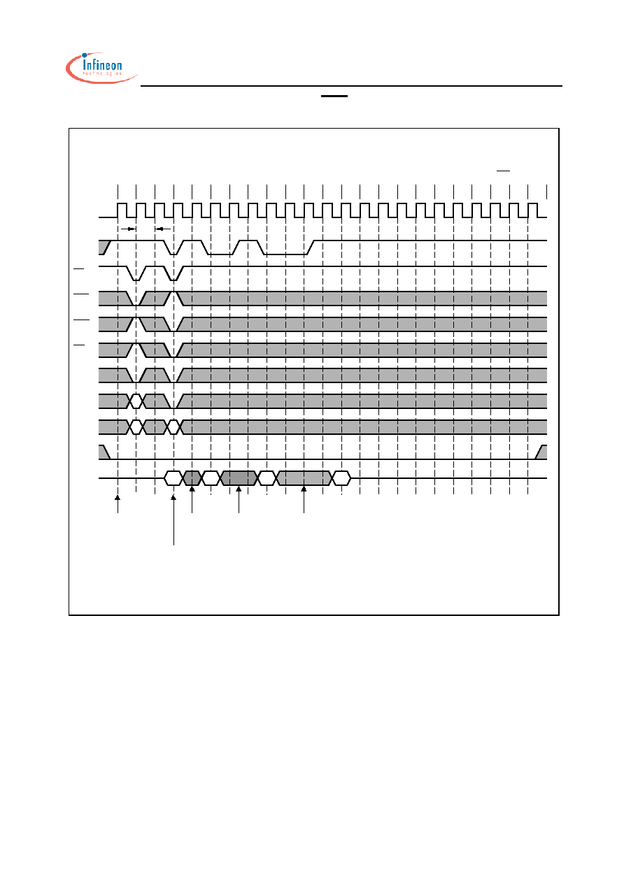
19. Random Row Write (Interleaving Banks) with Precharge
19.1 CAS Latency = 2
DBx4
DAx1
BS
AP
Addr.
DQ
DQM
Activate
Command
Bank A
Hi-Z
Write
Command
Bank A
DAx0
RAx
RAx
RCD
t
CAx
Command
Command
Bank B
Bank A
Command
DAx4
DAx2 DAx3
Bank B
Activate
DAx5 DAx6
RBx
RBx
Command
Precharge
Bank A
Write
DBx0
DAx7
DBx1
Activate
DBx2 DBx3
WR
CBx
t
RP
t
RAy
RAy
CLK
CKE
CS
RAS
CAS
WE
T0
High
CK2
t
T1
T2
T8
T4
T3
T5
T6
T7
T11
T9
T10
T12 T13
Command
Bank A
SPT03927
Command
Precharge
Bank B
DBx7
DBx5 DBx6
Write
DAy0 DAy1
CAy
WR
t
DAy4
DAy3
DAy2
T19
Burst Length = 8, CAS Latency = 2
T16
T15
T14
T17 T18
T20 T21 T22
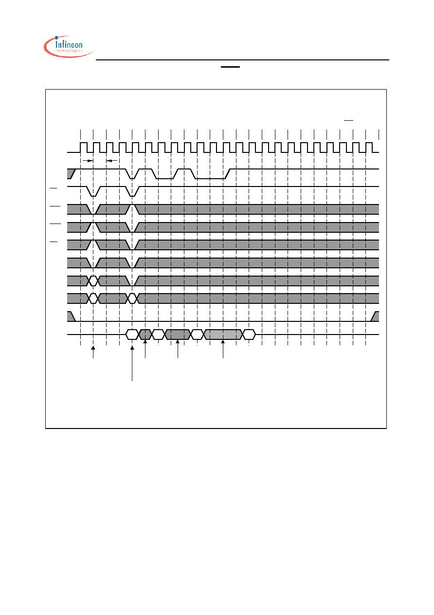
HYB39S64400/800/160BT(L)
64MBit Synchronous DRAM
Semiconductor Group
47
19.2 CAS Latency = 3
DAx4
Addr.
DQM
DQ
AP
BS
Command
Bank A
Bank A
Activate
Command
Hi-Z
Write
DAx0 DAx1
DAx3
DAx2
RAx
RCD
t
RAx
CAx
DBx4
DBx0
Write
Command
Bank B
Bank B
Activate
Command
DAx6
DAx5
DAx7
Precharge
Command
Bank A
DBx2
DBx1
DBx3
CBx
RBx
RBx
WR
t
RP
t
Command
Bank A
Activate
Command
Bank A
Write
DBx5 DBx6
DAy0
DBx7
Precharge
Bank B
Command
SPT03928
DAy1 DAy2 DAy3
WR
RAy
t
CAy
RAy
CAS
RAS
CKE
CLK
WE
CS
T2
High
CK3
t
T0
T1
T4
T3
T5
T6
T15
T7
T8
T9
T10 T11 T12 T13 T14
Burst Length = 8, CAS Latency = 3
T19
T17
T16
T18
T21
T20
T22

HYB39S64400/800/160BT(L)
64MBit Synchronous DRAM
Semiconductor Group
48
\
20. Full Page Read Cycle
20.1 CAS Latency = 2
BS
-
page address back to zero
from the highest order
The burst counter wraps
during this time interval.
Addr.
DQM
DQ
AP
~~
Hi-Z
Command
Command
Bank A
Read
Bank A
Activate
Bank B
Bank B
Command
Command
Ax
Activate
Activate
Ax
+1 Ax
~~
+ 2 Ax
RAx
RAx
CAx
~ ~
~ ~
RBx
RBx
~ ~
~ ~
~ ~
~ ~
SPT03929
bursting beginning with the starting address.
Burst Stop
Command
the burst counter increments and continues
terminate when the burst length is satisfied;
Full Page burst operation does not
Bank B
Command
Ax
Read
-
2
Ax 1
1
Ax+
Bx
Bx+1 Bx+2
+
Bx 3
+
Bx 4
CBx
Bank B
Command
Activate
Command
Bank B
Precharge
Bx
5
Bx+
6
+
RBy
t
RP
RBy
CAS
RAS
CKE
CLK
CS
WE
~ ~
~ ~
~ ~
~ ~
~ ~
~ ~
~ ~
High
CK2
t
T0
T1
T2
~ ~
~ ~
T3
T4
~ ~
~ ~
T5
T6
T15
T11
T7
T8
T10
T9
T13
T12
T14
Burst Length = Full Page, CAS Latency = 2
T16 T17 T18 T19 T20 T21 T22
HYB39S64400/800/160BT(L)
64MBit Synchronous DRAM
Semiconductor Group
49
20.2 CAS Latency = 3
T14
Bx
Full Page burst operation does not
terminate when the burst length is satisfied;
bursting beginning with the starting address.
the burst counter increments and continues
BS
Command
Bank A
AP
DQM
DQ
Addr.
Command
Activate
Bank A
Hi-Z
Read
RAx
RAx
CAx
page address back to zero
during this time interval.
The burst counter wraps
from the highest order
Activate
Activate
Bank B
Bank B
Command
Command
Ax
Ax 1
+
2
Ax +
Ax
~~
~~
-
RBx
RBx
~~
~~
~~
~~
~~
~~
Ax
Read
Bank B
Command
Ax
2
1
-
Ax
1
+
Bx
Bx 1
+
CBx
T3
CLK
CKE
CS
RAS
WE
CAS
T0
High
CK3
t
T1
T2
~~
~~
~~
~~
~~
~~
~~
T4
T5
~ ~~
~
~~
T7
T6
T8
~~
T10
T9
T11
T13
T12
SPT03930
Bank B
Command
Activate
Bank B
Precharge
Command
Burst Stop
Command
+
+2 Bx
Bx
3
4
+
5
+
Bx
RBy
t
RRD
RBy
T20
Burst Length = Full Page, CAS Latency = 3
T17
T15 T16
T18 T19
T21 T22

HYB39S64400/800/160BT(L)
64MBit Synchronous DRAM
Semiconductor Group
50
21. Full Page Write Cycle
21.1 CAS Latency = 2
T14
DBx
~ ~
Command
Activate
Command
Activate
Addr.
AP
DQM
DQ
Command
Bank A
Activate
Write
Command
Bank A
Hi-Z
RAx
RAx
DAx
DAx 1
+
CAx
page address back to zero
the burst counter increments and continues
bursting beginning with the starting address.
during this time interval.
CBx
DBx
Write
Bank B
terminate when the burst length is satisfied;
Command
from the highest order
The burst counter wraps
Bank B
Bank B
1
DAx
+
DAx 2
~~
~~
+3 DAx-
~~
RBx
RBx
~ ~~
~
~~
DAx
DAx+1
Full Page burst operation does not
Data is
ignored.
DBx
DBx+1
+
DBx 2
4
3
+
DBx+
DBx 5
+
T3
CLK
CKE
CS
CAS
RAS
BS
WE
T0
High
CK2
t
T1
T2
~ ~~
~
~~
~
~
~~
~
~
~~
~
~
~~
~~
T4
~~
T5
~~
T7
T6
T8
T10
T9
T11
T13
T12
SPT03931
Precharge
Command
Bank B
Burst Stop
Command
Command
Bank B
Activate
+6
RBy
RBy
T20
T17
T15 T16
T18 T19
T21 T22
Burst Length = Full Page, CAS Latency = 2
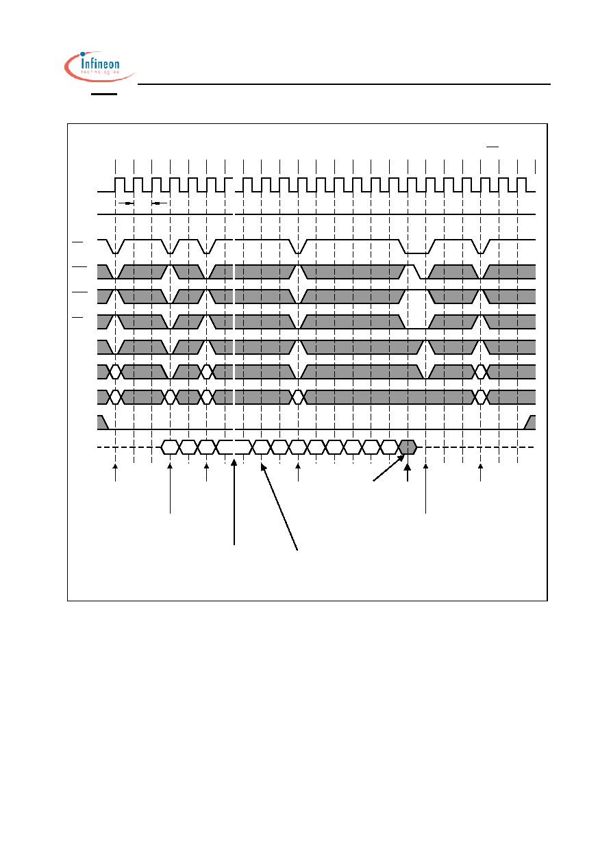
HYB39S64400/800/160BT(L)
64MBit Synchronous DRAM
Semiconductor Group
51
21.2 CAS Latency = 3
~ ~
terminate when the burst length is satisfied;
Command
bursting beginning with the starting address.
the burst counter increments and continues
page address back to zero
during this time interval.
DQ
DQM
Addr.
AP
Bank B
Bank B
from the highest order
The burst counter wraps
Command
Activate
Command
Activate
Write
Command
Bank A
Bank A
Command
Activate
Z
Hi
DAx
DAx+1
RAx
RAx
CAx
DAx
~~
DAx
+
DAx 2
~ ~
3
+
~ ~
DAx
-1
DAx 1
+
~ ~
RBx
~ ~
RBx
~ ~
SPT03932
Data is
ignored.
Full Page burst operation does not
Bank B
Write
Precharge
Bank B
Command
Burst Stop
Command
4
DBx
DBx
1
+
DBx
+
2
+
DBx
DBx
3
+
CBx
DBx+5
Command
Bank B
Activate
RBy
RBy
T8
BS
WE
CAS
RAS
CS
CKE
CLK
~ ~
~ ~
~ ~
~ ~
~ ~
~ ~
~ ~
~ ~
T3
High
T0
CK3
t
T1
T2
~ ~
~ ~
~ ~
T4
~ ~
T5
T6
T7
T18
T13
T9
T10 T11 T12
T15
T14
T16 T17
T20
T19
T21 T22
Burst Length = Full Page, CAS Latency = 3
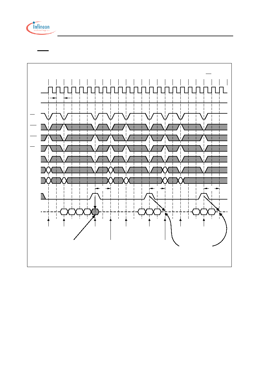
HYB39S64400/800/160BT(L)
64MBit Synchronous DRAM
Semiconductor Group
52
22. Precharge termination of a Burst
22.1 CAS Latency = 2
Command
Activate
Bank A
T14
BS
Write Data is masked.
of a Write Burst.
Precharge Termination
Addr.
DQ
DQM
AP
Command
Bank A
Activate
Hi Z
Bank A
Write
Command
DAx0 DAx1
RAx
RAx
CAx
Command
Bank A
Command
Precharge
Bank A
DAx3
DAx2
Activate
RAy
RP
t
RAy
Ay0
Command
Bank A
Read
Bank A
Precharge
Command
Ay1 Ay2
CAy
RP
t
T3
CS
WE
CAS
RAS
CKE
CLK
T0
High
CK2
t
T1
T2
T4
T5
T7
T6
T8
T10
T9
T11
T13
T12
Precharge Termination
of a Read Burst.
SPT03933
Bank A
Command
Precharge
Command
Bank A
Read
Az0 Az1
RAz
CAz
RAz
Az2
RP
t
Burst Length = 8 or Full Page, CAS Latency = 2
T20
T17
T15 T16
T18 T19
T21 T22