N e v e r s t o p t h i n k i n g .
M i c r o c o n t r o l l e r s
D a t a S h e e t , V 1 . 0 , A u g . 2 0 0 1
C 1 6 7 C S - x C , S t e p B A
1 6 - B i t S i n g l e - C h i p M i c r o c o n t r o l l e r
B a r e D i e D e l i v e r y

Edition 2001-08
Published by Infineon Technologies AG,
St.-Martin-Strasse 53,
D-81541 M¸nchen, Germany
©
Infineon Technologies AG 2001.
All Rights Reserved.
Attention please!
The information herein is given to describe certain components and shall not be considered as warranted
characteristics.
Terms of delivery and rights to technical change reserved.
We hereby disclaim any and all warranties, including but not limited to warranties of non-infringement, regarding
circuits, descriptions and charts stated herein.
Infineon Technologies is an approved CECC manufacturer.
Information
For further information on technology, delivery terms and conditions and prices please contact your nearest
Infineon Technologies Office in Germany or our Infineon Technologies Representatives worldwide (see address
list).
Warnings
Due to technical requirements components may contain dangerous substances. For information on the types in
question please contact your nearest Infineon Technologies Office.
Infineon Technologies Components may only be used in life-support devices or systems with the express written
approval of Infineon Technologies, if a failure of such components can reasonably be expected to cause the failure
of that life-support device or system, or to affect the safety or effectiveness of that device or system. Life support
devices or systems are intended to be implanted in the human body, or to support and/or maintain and sustain
and/or protect human life. If they fail, it is reasonable to assume that the health of the user or other persons may
be endangered.

M i c r o c o n t r o l l e r s
D a t a S h e e t , V 1 . 0 , A u g . 2 0 0 1
N e v e r s t o p t h i n k i n g .
C 1 6 7 C S - x C , S t e p B A
1 6 - B i t S i n g l e - C h i p M i c r o c o n t r o l l e r
B a r e D i e D e l i v e r y

Controller Area Network (CAN): License of Robert Bosch GmbH
C167CS-xC
(Bare Die Delivery)
Revision History:
2001-08
V1.0
Previous Version:
-
Page
Subjects (major changes since last revision)
We Listen to Your Comments
Any information within this document that you feel is wrong, unclear or missing at all?
Your feedback will help us to continuously improve the quality of this document.
Please send your proposal (including a reference to this document) to:
mcdocu.comments@infineon.com

Data Sheet
1
V1.0, 2001-08
C167CS-xC
16-Bit Single-Chip Microcontroller
C166 Family
C167CS-xC
∑ High Performance 16-bit CPU with 4-Stage Pipeline
≠ 80/60 ns Instruction Cycle Time at 25/33 MHz CPU Clock
≠ 400/303 ns Multiplication (16
◊ 16 bit), 800/606 ns Division (32/16 bit)
≠ Enhanced Boolean Bit Manipulation Facilities
≠ Additional Instructions to Support HLL and Operating Systems
≠ Register-Based Design with Multiple Variable Register Banks
≠ Single-Cycle Context Switching Support
≠ 16 MBytes Total Linear Address Space for Code and Data
≠ 1024 Bytes On-Chip Special Function Register Area
∑ 16-Priority-Level Interrupt System with 56 Sources, Sample-Rate down to 40/30 ns
∑ 8-Channel Interrupt-Driven Single-Cycle Data Transfer Facilities via
Peripheral Event Controller (PEC)
∑ Clock Generation via on-chip PLL (factors 1:1.5/2/2.5/3/4/5),
via prescaler or via direct clock input
∑ On-Chip Memory Modules
≠ 3 KBytes On-Chip Internal RAM (IRAM)
≠ 8 KBytes On-Chip Extension RAM (XRAM)
≠ 32 KBytes On-Chip Program Mask ROM
∑ On-Chip Peripheral Modules
≠ 24-Channel 10-bit A/D Converter with Programmable Conversion Time
down to 7.8
µs
≠ Two 16-Channel Capture/Compare Units
≠ 4-Channel PWM Unit
≠ Two Multi-Functional General Purpose Timer Units with 5 Timers
≠ Two Serial Channels (Synchronous/Asynchronous and High-Speed-Synchronous)
≠ Two On-Chip CAN Interfaces (Rev. 2.0B active) with 2
◊ 15 Message Objects
(Full CAN/Basic CAN), can work on one bus with 30 objects
≠ On-Chip Real Time Clock
∑ Up to 16 MBytes External Address Space for Code and Data
≠ Programmable External Bus Characteristics for Different Address Ranges
≠ Multiplexed or Demultiplexed External Address/Data Buses with 8-Bit or 16-Bit
Data Bus Width
≠ Five Programmable Chip-Select Signals
≠ Hold- and Hold-Acknowledge Bus Arbitration Support
∑ Idle, Sleep, and Power Down Modes with Flexible Power Management
∑ Programmable Watchdog Timer and Oscillator Watchdog
∑ Up to 111 General Purpose I/O Lines,
partly with Selectable Input Thresholds and Hysteresis
C167CS-xC Bare Die
Step BA
Data Sheet
2
V1.0, 2001-08
∑ Supported by a Large Range of Development Tools like C-Compilers,
Macro-Assembler Packages, Emulators, Evaluation Boards, HLL-Debuggers,
Simulators, Logic Analyzer Disassemblers, Programming Boards
∑ On-Chip Bootstrap Loader
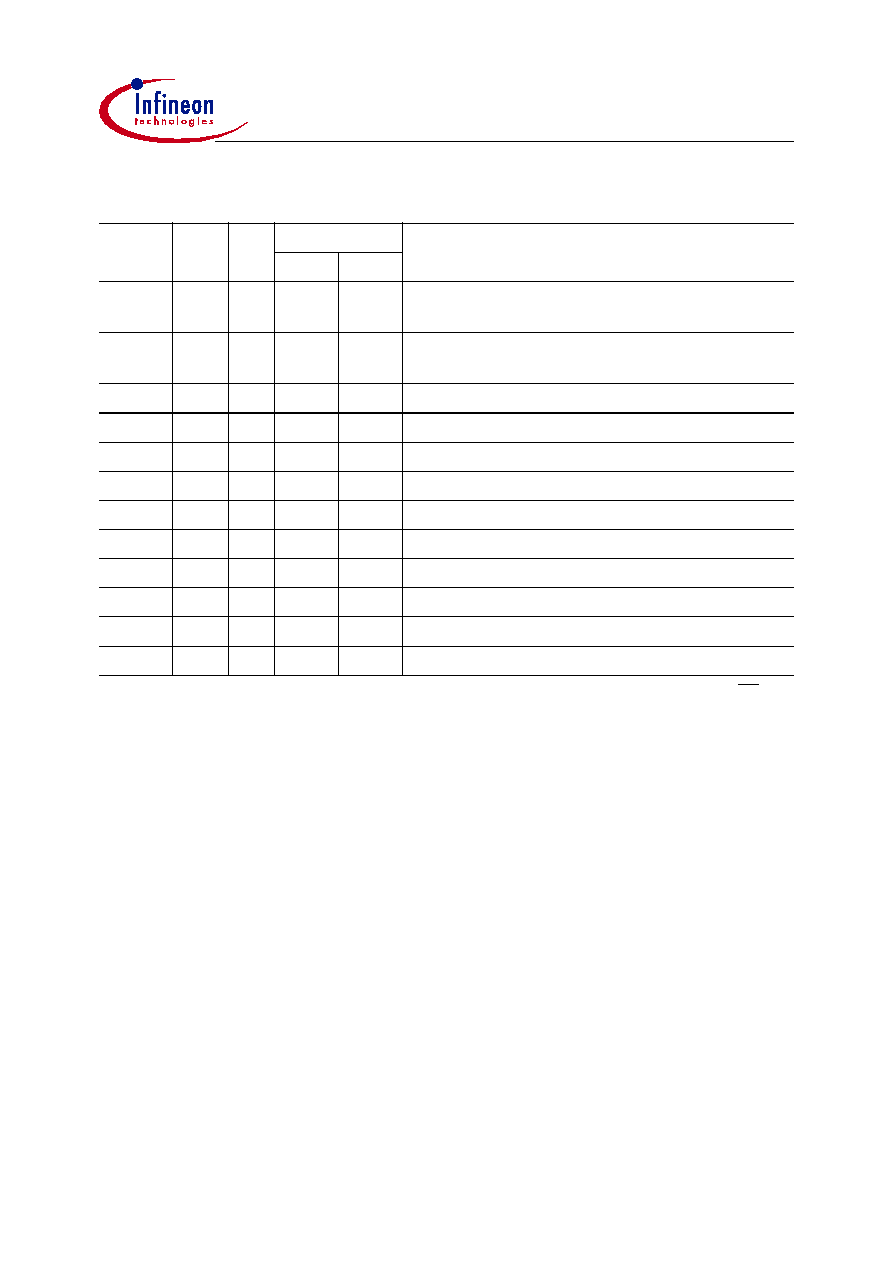
This document describes several derivatives of the C167 group.
Table 1
enumerates
these derivatives and summarizes the differences. As this document refers to all of these
derivatives, some descriptions may not apply to a specific product.
Note: The ordering codes for Mask-ROM versions are defined for each product after
verification of the respective ROM code.
For simplicity all versions are referred to by the term C167CS-xC throughout this
document.
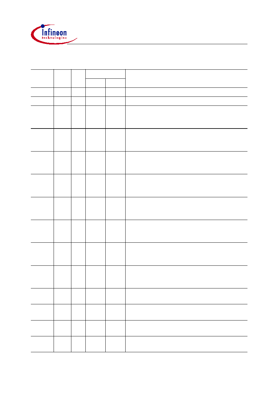
Table 1
C167CS-xC Bare Die Derivative Synopsis
Type
Ordering
Code
Program
Memory
Operating
Temperature
Wafers
SAK-C167CS-4RC
Q67120-
D....
32 KByte ROM
-40 to +125 ∞C
Whole
SAK-C167CS-LC
Q67120-
C2200
---
-40 to +125 ∞C
Sawn
SAL-C167CS-LC
1)
1)
The designation SAL-
... conforms to the valid ProElectron specification. These devices were named SAA-...
formerly.
Q67120-
C2274
---
-40 to +150 ∞C
Sawn
SAL-C167CS-L33C
1)
Q67120-
C2275
---
-40 to +150 ∞C
Sawn
C167CS-xC Bare Die
Step BA
Data Sheet
3
V1.0, 2001-08
Introduction
The C167CS-xC derivatives are high performance derivatives of the Infineon
C166 Family of full featured single-chip CMOS microcontrollers. They combine high
CPU performance (up to 16.5 million instructions per second) with high peripheral
functionality and enhanced IO-capabilities. They also provide clock generation via PLL
and various on-chip memory modules such as program ROM, internal RAM, and
extension RAM.
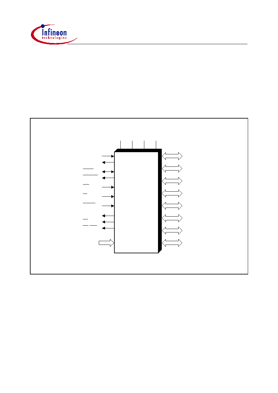
Figure 1
Logic Symbol
MCL04411
XTAL1
XTAL2
RSTOUT
ALE
NMI
RD
RSTIN
Port 0
16 Bit
16 Bit
Port 1
16 Bit
Port 2
15 Bit
Port 3
8 Bit
Port 4
V
AREF
AGND
V
WR/WRL
Port 5
16 Bit
Port 6
8 Bit
EA
READY
Port 7
8 Bit
8 Bit
Port 8
DD
V
SS
V
C167CS-xC

C167CS-xC Bare Die
Step BA
Data Sheet
4
V1.0, 2001-08
Pad Configuration
(top view)
Figure 2
Several pins of Port 4 and Port 8 can have CAN interface lines assigned to them.
Table 2
on the following pages lists the possible assignments.
C167CS-xC
Pad 1
Pad
1
46
y
x
0.0
0.0
Pad 36
Pad
3
7
Pa
d
7
3
P
a
d
111
Pad 110
Pad 74
Position of
Logo and Marking
C167CS-xC Bare Die
Step BA
Data Sheet
5
V1.0, 2001-08
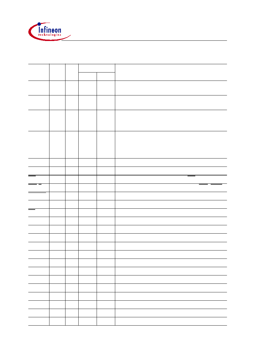
Table 2
Pad Definitions and Functions
Symbol Pad
Num
In /
Out
Position [µm] Function
x
y
9
AREF
1
-
305
0 Reference voltage for the A/D converter.
9
AGND
2
-
460
0 Reference ground for the A/D converter.
P5.10
3
I
615
0 Port 5 input, analog input AN10,
external up/down T6EUD.
P5.11
4
I
770
0 Port 5 input, analog input AN11,
external up/down T5EUD.
P5.12
5
I
925
0 Port 5 input, analog input AN12,
timer input T6IN.
P5.13
6
I
1081
0 Port 5 input, analog input AN13,
timer input T5IN.
P5.14
7
I
1236
0 Port 5 input, analog input AN14,
external up/down T4EUD.
P5.15
8
I
1391
0 Port 5 input, analog input AN15,
external up/down T2EUD.
9
SS
9
-
1563
0 Digital Ground.
9
DD
10
-
1688
0 Digital Supply Voltage.
P2.0
11
I/O
1960
0 Port 2 input/output (open drain, sp. threshold),
Capture-Input/Compare-Output CC0IO.
P2.1
12
I/O
2139
0 Port 2 input/output (open drain, sp. threshold),
Capture-Input/Compare-Output CC1IO.
P2.2
13
I/O
2318
0 Port 2 input/output (open drain, sp. threshold),
Capture-Input/Compare-Output CC2IO.
P2.3
14
I/O
2497
0 Port 2 input/output (open drain, sp. threshold),
Capture-Input/Compare-Output CC3IO.
P2.4
15
I/O
2676
0 Port 2 input/output (open drain, sp. threshold),
Capture-Input/Compare-Output CC4IO.
P2.5
16
I/O
2855
0 Port 2 input/output (open drain, sp. threshold),
Capture-Input/Compare-Output CC5IO.
P2.6
17
I/O
3034
0 Port 2 input/output (open drain, sp. threshold),
Capture-Input/Compare-Output CC6IO.
P2.7
18
I/O
3214
0 Port 2 input/output (open drain, sp. threshold),
Capture-Input/Compare-Output CC7IO.
C167CS-xC Bare Die
Step BA
Data Sheet
6
V1.0, 2001-08
9
SS
19
-
3393
0 Digital Ground.
9
DD
20
-
3572
0 Digital Supply Voltage.
P2.8
21
I/O
3751
0 Port 2 input/output (open drain, sp. threshold),
Capt. Input/Comp. Output CC8IO,
Fast Interrupt EX0IN.
P2.9
22
I/O
3930
0 Port 2 input/output (open drain, sp. threshold),
Capt. Input/Comp. Output CC9IO,
Fast Interrupt EX1IN.
P2.10
23
I/O
4109
0 Port 2 input/output (open drain, sp. threshold),
Capt. Input/Comp. Output CC10IO,
Fast Interrupt EX2IN.
P2.11
24
I/O
4288
0 Port 2 input/output (open drain, sp. threshold),
Capt. Input/Comp. Output CC11IO,
Fast Interrupt EX3IN.
P2.12
25
I/O
4467
0 Port 2 input/output (open drain, sp. threshold),
Capt. Input/Comp. Output CC12IO,
Fast Interrupt EX4IN.
P2.13
26
I/O
4646
0 Port 2 input/output (open drain, sp. threshold),
Capt. Input/Comp. Output CC13IO,
Fast Interrupt EX5IN.
P2.14
27
I/O
4826
0 Port 2 input/output (open drain, sp. threshold),
Capt. Input/Comp. Output CC14IO,
Fast Interrupt EX6IN.
P2.15
28
I/O
5005
0 Port 2 input/output (open drain, sp. threshold),
Capt. Input/Comp. Output CC15IO,
Fast Interrupt EX7IN, Timer T7 input T7IN.
P3.0
29
I/O
5184
0 Port 3 input/output (open drain, sp. threshold),
Timer T0 Input T0IN.
P3.1
30
I/O
5363
0 Port 3 input/output (open drain, sp. threshold),
Timer T6 Toggle Latch Output T6OUT.
P3.2
31
I/O
5542
0 Port 3 input/output (open drain, sp. threshold),
CAPREL Capture Input CAPIN.
P3.3
32
I/O
5721
0 Port 3 input/output (open drain, sp. threshold),
Timer T3 Toggle Latch Output T3OUT.
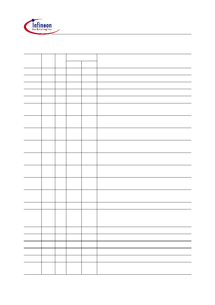
Table 2
Pad Definitions and Functions (cont'd)
Symbol Pad
Num
In /
Out
Position [µm] Function
x
y

C167CS-xC Bare Die
Step BA
Data Sheet
7
V1.0, 2001-08
P3.4
33
I/O
5900
0 Port 3 input/output (open drain, sp. threshold),
Timer T3 ext.up/down T3EUD.
P3.5
34
I/O
6079
0 Port 3 input/output (open drain, sp. threshold),
Timer T4 Input T4IN.
9
SS
35
-
6258
0 Digital Ground.
9
DD
36
-
6437
0 Digital Supply Voltage.
P3.6
37
I/O
6936
498 Port 3 input/output (open drain, sp. threshold),
Timer T3 Input T3IN.
P3.7
38
I/O
6936
695 Port 3 input/output (open drain, sp. threshold),
Timer T2 Input T2IN.
P3.8
39
I/O
6936
892 Port 3 input/output (open drain, sp. threshold),
SSC Master-Rec./Slave-Transmit I/O MRST.
P3.9
40
I/O
6936
1090 Port 3 input/output (open drain, sp. threshold),
SSC Master-Transmit/Slave-Rec. O/I MTSR.
P3.10
41
I/O
6936
1287 Port 3 input/output (open drain, sp. threshold),
ASC0 Clock/Data Output (Asyn./Syn.) TxD0.
P3.11
42
I/O
6936
1484 Port 3 input/output (open drain, sp. threshold),
ASC0 Data Input (Asyn.) or I/O (Syn.) RxD0.
P3.12
43
I/O
6936
1681 Port 3 input/output (open drain, sp. threshold).
44
O
6936
1878 High Byte Enable BHE,
High Byte Write Strobe WRH.
P3.13
45
I/O
6936
2075 Port 3 input/output (open drain, sp. threshold),
SSC Master(Slave) Clock Output(Input) SCLK.
P3.15
46
I/O
6936
2272 Port 3 input/output (open drain, sp. threshold).
47
O
6936
2469 System Clock Output (=CPU Clock) CLKOUT,
Programmable Frequency Output FOUT.
9
DD
48
-
6936
2666 Digital Supply Voltage.
9
SS
49
-
6936
2837 Digital Ground.
P4.0
50
I/O
6936
2993 Port 4 input/output, Segment Address Line A16.
P4.1
51
I/O
6936
3149 Port 4 input/output, Segment Address Line A17.
P4.2
52
I/O
6936
3306 Port 4 input/output, Segment Address Line A18.
P4.3
53
I/O
6936
3462 Port 4 input/output, Segment Address Line A19.
Table 2
Pad Definitions and Functions (cont'd)
Symbol Pad
Num
In /
Out
Position [µm] Function
x
y
C167CS-xC Bare Die
Step BA
Data Sheet
8
V1.0, 2001-08
P4.4
54
I/O
6936
3618 Port 4 input/output, Segment Address Line A20,
CAN2 Receive Data Input CAN2_RxD.
P4.5
55
I/O
6936
3775 Port 4 input/output, Segment Address Line A21,
CAN1 Receive Data Input CAN1_RxD.
P4.6
56
I/O
6936
3931 Port 4 input/output, Segment Address Line A22
CAN1 Transmit Data Output CAN1_TxD
CAN2 Transmit Data Output CAN2_TxD.
P4.7
57
I/O
6936
4087 Port 4 input/output, Segment Address Line A23,
CAN1 Receive Data Input CAN1_RxD
CAN2 Transmit Data Output CAN2_TxD,
CAN2 Receive Data Input CAN2_RxD.
9
DD
58
-
6936
4244 Digital Supply Voltage.
9
SS
59
-
6936
4400 Digital Ground.
RD
60
O
6936
4556 External Memory Read Strobe RD.
WR(L)
61
O
6936
4712 External Memory Write(Low) Strobe WR (WRL).
READY
62
I
6936
4869 Ready Input.
ALE
63
O
6936
5025 Address Latch Enable Output.
EA
64
I
6936
5181 External Access Enable pin.
P0L.0
65
I/O
6936
5338 PORT0 input/output, Address/Data Line AD0.
P0L.1
66
I/O
6936
5494 PORT0 input/output, Address/Data Line AD1.
P0L.2
67
I/O
6936
5650 PORT0 input/output, Address/Data Line AD2.
P0L.3
68
I/O
6936
5807 PORT0 input/output, Address/Data Line AD3.
P0L.4
69
I/O
6936
5963 PORT0 input/output, Address/Data Line AD4.
P0L.5
70
I/O
6936
6119 PORT0 input/output, Address/Data Line AD5.
P0L.6
71
I/O
6936
6275 PORT0 input/output, Address/Data Line AD6.
P0L.7
72
I/O
6936
6432 PORT0 input/output, Address/Data Line AD7.
P0H.0
73
I/O
6936
6588 PORT0 input/output, Address/Data Line AD8.
9
DD
74
-
6437
7086 Digital Supply Voltage.
9
SS
75
-
6274
7086 Digital Ground.
P0H.1
76
I/O
6110
7086 PORT0 input/output, Address/Data Line AD9.
P0H.2
77
I/O
5947
7086 PORT0 input/output, Address/Data Line AD10.
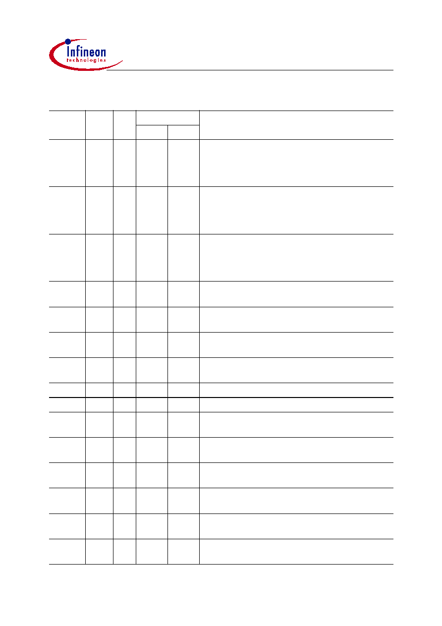
Table 2
Pad Definitions and Functions (cont'd)
Symbol Pad
Num
In /
Out
Position [µm] Function
x
y
C167CS-xC Bare Die
Step BA
Data Sheet
9
V1.0, 2001-08
P0H.3
78
I/O
5783
7086 PORT0 input/output, Address/Data Line AD11.
P0H.4
79
I/O
5620
7086 PORT0 input/output, Address/Data Line AD12.
P0H.5
80
I/O
5456
7086 PORT0 input/output, Address/Data Line AD13.
P0H.6
81
I/O
5293
7086 PORT0 input/output, Address/Data Line AD14.
P0H.7
82
I/O
5129
7086 PORT0 input/output, Address/Data Line AD15.
P1L.0
83
I/O
4966
7086 PORT1 input/output, Address Line A0,
analog input AN16.
P1L.1
84
I/O
4802
7086 PORT1 input/output, Address Line A1,
analog input AN17.
P1L.2
85
I/O
4639
7086 PORT1 input/output, Address Line A2,
analog input AN18.
P1L.3
86
I/O
4475
7086 PORT1 input/output, Address Line A3,
analog input AN19.
P1L.4
87
I/O
4312
7086 PORT1 input/output, Address Line A4,
analog input AN20.
P1L.5
88
I/O
4148
7086 PORT1 input/output, Address Line A5,
analog input AN21.
P1L.6
89
I/O
3985
7086 PORT1 input/output, Address Line A6,
analog input AN22.
P1L.7
90
I/O
3821
7086 PORT1 input/output, Address Line A7,
analog input AN23.
9
DD
91
-
3658
7086 Digital Supply Voltage.
C167CS
MODE
92
I
3494
7086 Must be connected to
9
DD
.
1)
Standard oscillator mode, single-chip reset with
PORT0-configuration.
9
SS
93
-
3331
7086 Digital Ground.
P1H.0
94
I/O
3167
7086 PORT1 input/output, Address Line A8.
P1H.1
95
I/O
3004
7086 PORT1 input/output, Address Line A9.
P1H.2
96
I/O
2840
7086 PORT1 input/output, Address Line A10.
P1H.3
97
I/O
2677
7086 PORT1 input/output, Address Line A11.
P1H.4
98
I/O
2513
7086 PORT1 input/output, Addr. Line A12,
Capt. Input/Comp. Output CC24.
Table 2
Pad Definitions and Functions (cont'd)
Symbol Pad
Num
In /
Out
Position [µm] Function
x
y

C167CS-xC Bare Die
Step BA
Data Sheet
10
V1.0, 2001-08
P1H.5
99
I/O
2350
7086 PORT1 input/output, Addr. Line A13,
Capt. Input/Comp. Output CC25.
P1H.6
100
I/O
2186
7086 PORT1 input/output, Addr. Line A14,
Capt. Input/Comp. Output CC26.
P1H.7
101
I/O
2023
7086 PORT1 input/output, Addr. Line A15,
Capt. Input/Comp. Output CC27.
9
DD
102
-
1859
7086 Digital Supply Voltage.
XTAL2
103
O
1708
7086 Output of the oscillator amplifier circuit.
XTAL1
104
I
1479
7086 Input to oscillator amplifier and internal clock
generator.
9
SS
105
-
1316
7086 Digital Ground.
RSTIN
106
I/O
1152
7086 Reset Input with Schmitt-Trigger characteristics,
output in bidirectional reset mode.
RST
OUT
107
O
989
7086 Internal Reset Indication Output.
NMI
108
I
825
7086 Non-Maskable Interrupt Input.
9
SS
109
-
662
7086 Digital Ground.
9
DD
110
-
498
7086 Digital Supply Voltage.
P6.0
111
I/O
0
6588 Port 6 input/output, Chip Select 0 Output CS0.
P6.1
112
I/O
0
6404 Port 6 input/output, Chip Select 1 Output CS1.
P6.2
113
I/O
0
6220 Port 6 input/output, Chip Select 2 Output CS2.
P6.3
114
I/O
0
6036 Port 6 input/output, Chip Select 3 Output CS3.
P6.4
115
I/O
0
5852 Port 6 input/output, Chip Select 4 Output CS4.
P6.5
116
I/O
0
5668 Port 6 input/output,
External Hold Request Input HOLD.
P6.6
117
I/O
0
5485 Port 6 input/output,
External Hold Acknowledge Output HLDA.
P6.7
118
I/O
0
5301 Port 6 input/output, Bus Request Output BREQ.
P8.0
119
I/O
0
5117 Port 8 input/output,
Capt.-Input/Comp.-Output CC16IO,
CAN1 Receive Data Input CAN1_RxD,
CAN2 Receive Data Input CAN2_RxD.
Table 2
Pad Definitions and Functions (cont'd)
Symbol Pad
Num
In /
Out
Position [µm] Function
x
y
C167CS-xC Bare Die
Step BA
Data Sheet
11
V1.0, 2001-08
P8.1
120
I/O
0
4933 Port 8 input/output,
Capt.-Input/Comp.-Output CC17IO,
CAN1 Transmit Data Output CAN1_TxD,
CAN2 Transmit Data Output CAN2_TxD.
P8.2
121
I/O
0
4749 Port 8 input/output,
Capt.-Input/Comp.-Output CC18IO,
CAN1 Receive Data Input CAN1_RxD,
CAN2 Receive Data Input CAN2_RxD.
P8.3
122
I/O
0
4565 Port 8 input/output,
Capt.-Input/Comp.-Output CC19IO,
CAN1 Transmit Data Output CAN1_TxD,
CAN2 Transmit Data Output CAN2_TxD.
P8.4
123
I/O
0
4381 Port 8 input/output,
Capt.-Input/Comp.-Output CC20IO.
P8.5
124
I/O
0
4197 Port 8 input/output,
Capt.-Input/Comp.-Output CC21IO.
P8.6
125
I/O
0
4013 Port 8 input/output,
Capt.-Input/Comp.-Output CC22IO.
P8.7
126
I/O
0
3829 Port 8 input/output,
Capt.-Input/Comp.-Output CC23IO.
9
DD
127
-
0
3646 Digital Supply Voltage.
9
SS
128
-
0
3462 Digital Ground.
P7.0
129
I/O
0
3278 Port 7 input/output, (open drain, sp. threshold),
PWM Channel Output POUT0.
P7.1
130
I/O
0
3094 Port 7 input/output, (open drain, sp. threshold),
PWM Channel Output POUT1.
P7.2
131
I/O
0
2910 Port 7 input/output, (open drain, sp. threshold),
PWM Channel Output POUT2.
P7.3
132
I/O
0
2726 Port 7 input/output, (open drain, sp. threshold),
PWM Channel Output POUT3.
P7.4
133
I/O
0
2542 Port 7 input/output, (open drain, sp. threshold),
Capt.-Input/Comp.-Output CC28IO.
P7.5
134
I/O
0
2358 Port 7 input/output, (open drain, sp. threshold),
Capt.-Input/Comp.-Output CC29IO.
Table 2
Pad Definitions and Functions (cont'd)
Symbol Pad
Num
In /
Out
Position [µm] Function
x
y
C167CS-xC Bare Die
Step BA
Data Sheet
12
V1.0, 2001-08
Note: All
9
SS
pads and all
9
DD
pads must be connected to the system ground and the
power supply, respectively.
The pad definitions and locations in this table are only valid for the indicated device
and design step.
P7.6
135
I/O
0
2174 Port 7 input/output, (open drain, sp. threshold),
Capt.-Input/Comp.-Output CC30IO.
P7.7
136
I/O
0
1990 Port 7 input/output, (open drain, sp. threshold),
Capt.-Input/Comp.-Output CC31IO.
P5.0
137
I
0
1701 Port 5 input, analog input AN0.
P5.1
138
I
0
1546 Port 5 input, analog input AN1.
P5.2
139
I
0
1391 Port 5 input, analog input AN2.
P5.3
140
I
0
1236 Port 5 input, analog input AN3.
P5.4
141
I
0
1081 Port 5 input, analog input AN4.
P5.5
142
I
0
925 Port 5 input, analog input AN5.
P5.6
143
I
0
770 Port 5 input, analog input AN6.
P5.7
144
I
0
615 Port 5 input, analog input AN7.
P5.8
145
I
0
460 Port 5 input, analog input AN8.
P5.9
146
I
0
305 Port 5 input, analog input AN9.
1)
Prepared to enable Enhanced Mode, i.e. low-power oscillator mode, single-chip reset with RD/ALE-
configuration.
Table 2
Pad Definitions and Functions (cont'd)
Symbol Pad
Num
In /
Out
Position [µm] Function
x
y
C167CS-xC Bare Die
Step BA
Data Sheet
13
V1.0, 2001-08
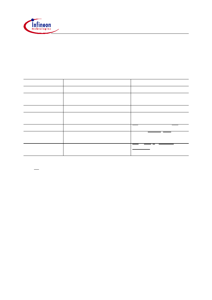
Handling Of Unconnected Pads
Signal input stages may generate undesired switching noise and cross-current when left
open. Respect the following precautions for unconnected (not bonded) pads:
Table 3
Precautions for Unconnected Pads
Pad Type
Recommended Action
Related Pads
Power Supply
Always connect!
9
DD
,
9
SS
,
9
AREF
,
9
AGND
Standard IO pads
Switch to output
PORT0, PORT1
1)
, P2, P3,
P4, P6, P7, P8
1)
The lower part of PORT1 (P1L) may be left open and its input stages can then be disabled via P1DIDIS.
Input port pads
Disable input stages via P5DIDIS
P5
Double-bond ports
Connect port pad (43, 46), if the
alternate output (44, 47) is used.
2)
2)
Port pad is input in this case! If the port pad is used, the corresponding alternate output pad may be left open.
P3.12 (43/44), P3.15 (46/47)
Configuration lines
Always connect!
EA, C167CSMODE, RD
3)
3)
Pin RD can be used for configuration to disable the OWD. Otherwise it is held high by an internal pullup.
Required
control lines
Always connect!
XTAL1, RSTIN, NMI
Optional
control lines
Can be left open
RD
3)
, WR(L), READY, ALE,
RSTOUT
C167CS-xC Bare Die
Step BA
Data Sheet
14
V1.0, 2001-08
Functional Description
As the standard packaged devices are made from this silicon the C167CS-xC dies
provide exactly the same functionality and behaviour. Also the DC characteristics and
AC characteristics are compatible with those of the packaged devices.
For a description of the functionality and the DC and AC parameters please refer to the
following documents (or later versions thereof):
∑ C167CS-4R/-L Data Sheet, Version 2.2, 2001-08
∑ C167CS Derivatives User's Manual, Version 2.0, 2000-07
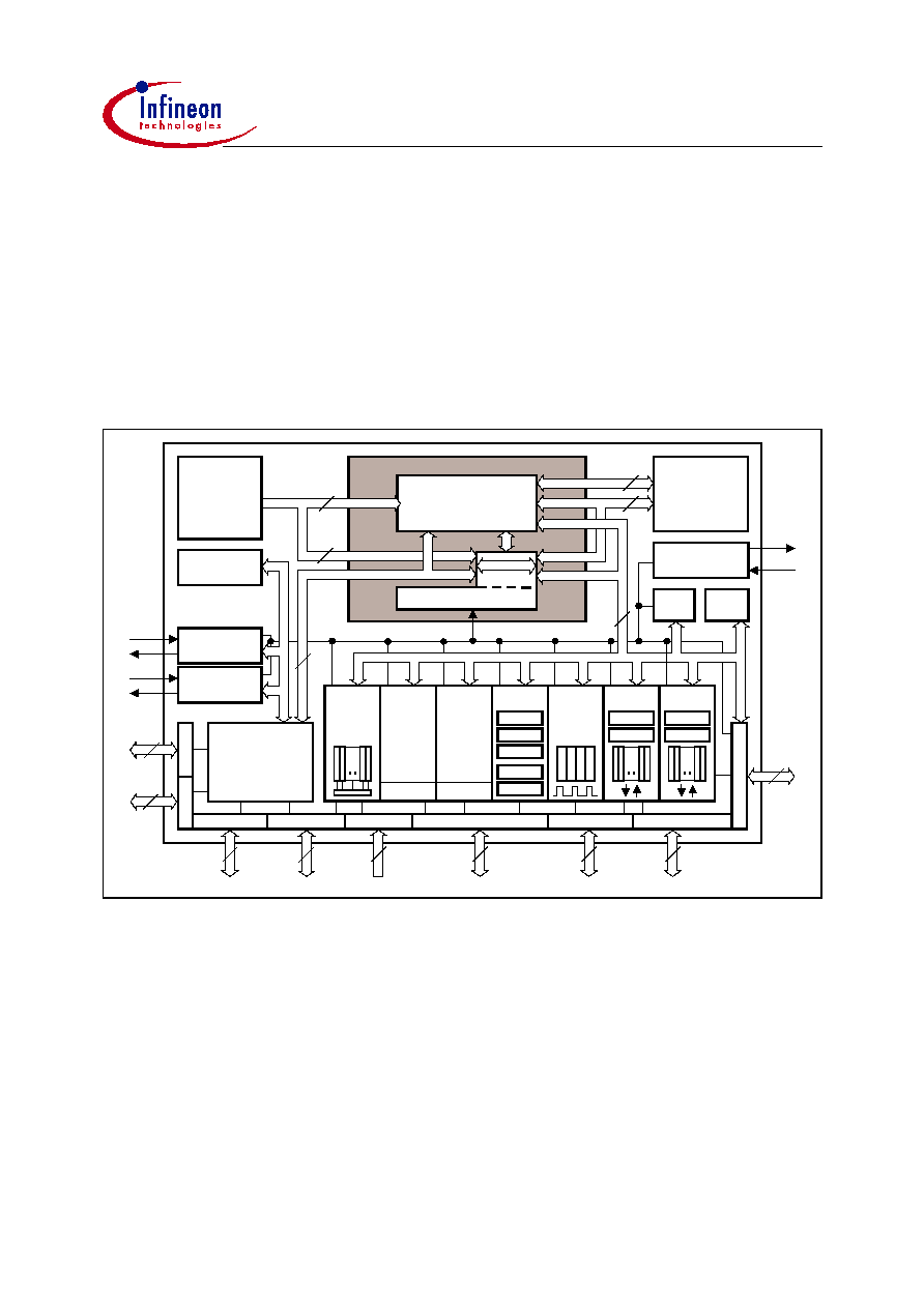
Figure 3
Block Diagram
C166-Core
CPU
Port 2
Interrupt Bus
XTAL
Osc / PLL
RTC
WDT
32
16
Interrupt Controller 16-Level
Priority
PEC
External Instr. / Data
GPT
T2
T3
T4
T5
T6
SSC
BRGen
(SPI)
ASC0
BRGen
(USART)
ADC
10-Bit
16+8
Channels
PWM
CCOM1
T0
T1
CCOM2
T7
T8
EBC
XBUS Control
External Bus
Control
IRAM
Dual Port
Internal
RAM
3 KByte
ProgMem
ROM
32 KByte
Data
Data
16
16
16
CAN1
Rev 2.0B active
Instr. / Data
Port 0
XRAM
6+2 KByte
Port 6
8
8
Port 1
16
16
16
Port 5
Port 3
15
Port 7
8
Port 8
8
Port 4
16
Peripheral Data Bus
16
CAN2
Rev 2.0B active
On-Chip XBUS (16-Bit Demux)
MCB04323_7CS

C167CS-xC Bare Die
Step BA
Data Sheet
15
V1.0, 2001-08
Absolute Maximum Ratings
Note: Stresses above those listed under "Absolute Maximum Ratings" may cause
permanent damage to the device. This is a stress rating only and functional
operation of the device at these or any other conditions above those indicated in
the operational sections of this specification is not implied. Exposure to absolute
maximum rating conditions for extended periods may affect device reliability.
During absolute maximum rating overload conditions (
9
IN
>
9
DD
or
9
IN
<
9
SS
) the
voltage on
9
DD
pins with respect to ground (
9
SS
) must not exceed the values
defined by the absolute maximum ratings.
Storage Conditions
The C167CS-xC dies may be stored for a certain time under the conditions described
below.
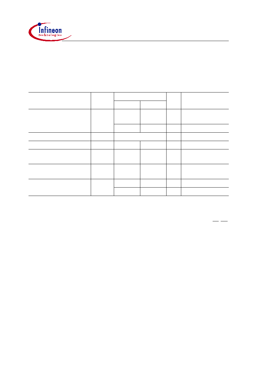
Table 4
Absolute Maximum Rating Parameters
Parameter
Symbol
Limit Values
Unit Notes
min.
max.
Storage temperature
7
ST
-65
150
∞C
Junction temperature
7
J
-40
150
∞C
under bias
Voltage on
9
DD
pins with
respect to ground (
9
SS
)
9
DD
-0.5
6.5
V
Voltage on any pin with
respect to ground (
9
SS
)
9
IN
-0.5
9
DD
+ 0.5 V
Input current on any pin
during overload condition
-10
10
mA
Absolute sum of all input
currents during overload
condition
-
|100|
mA
Table 5
Bare Die Storage Conditions and Duration
Packing
Environment
Temperature
Rel. Humidity
Storage Time
Vacuum pack
Air
15
... 30 ∞C
< 60 %
< 4 Months
C167CS-xC Bare Die
Step BA
Data Sheet
16
V1.0, 2001-08
Operating Conditions
The following operating conditions must not be exceeded in order to ensure correct
operation of the C167CS-xC. All parameters specified in the following sections refer to
these operating conditions, unless otherwise noticed.
Table 6
Operating Condition Parameters
Parameter
Symbol
Limit Values
Unit Notes
min.
max.
Digital supply voltage
9
DD
4.5
5.5
V
Active mode,
I
CPUmax
= 33 MHz
2.5
1)
1)
Output voltages and output currents will be reduced when
9
DD
leaves the range defined for active mode.
5.5
V
PowerDown mode
Digital ground voltage
9
SS
0
V
Reference voltage
Overload current
,
OV
-
±5
mA
Per pin
2)
3)
2)
Overload conditions occur if the standard operatings conditions are exceeded, i.e. the voltage on any pin
exceeds the specified range (i.e.
9
OV
!
9
DD
+0.5V or
9
OV
9
SS
-0.5V). The absolute sum of input overload
currents on all pins may not exceed 50 mA. The supply voltage must remain within the specified limits.
Proper operation is not guaranteed if overload conditions occur on functional pins such as XTAL1, RD, WR,
etc.
3)
Not 100% tested, guaranteed by design and characterization.
Absolute sum of overload
currents
|
,
OV
|
-
50
mA
3)
External Load
Capacitance
&
L
-
50
pF
Pin drivers in
fast edge mode
4)
4)
The timing is valid for pin drivers in high current or dynamic current mode. The reduced static output current in
dynamic current mode must be respected when designing the system.
Temperature of the
bottom side of the die
7
D
-40
150
∞C
SAL-C167CS-xC...
-40
125
∞C
SAK-C167CS-xC...

C167CS-xC Bare Die
Step BA
Data Sheet
17
V1.0, 2001-08
Chip Outline
Figure 4
0.38
7.44
7.29
Dimensions in mm
0.090
0.090 0.125
x
y
0,0
min
Typical

C167CS-xC Bare Die
Step BA
Data Sheet
18
V1.0, 2001-08
The wafers are glued to a plastic tape which is fixed within a plastic ring (see
Figure 5
).
Wafers can be shipped in one piece or sawn into individual dies.
Note: Please refer also to the document "Bare Die Packing Information".
Table 7
Wafer Characteristics
Item
Characteristic
Chips per wafer
262 (geometrically)
Metallization layers
2
Metallization material
AlCu
Metallization thickness
Met1: 450 nm, Met2: 800 nm
Metallization barrier material
Ti
Metallization isolation
SOG-CMP
Metallization material on pads
AlSiCu (Al 98.5% - SI 1% - Cu 0.5%)
Passivation
Oxide (300 nm) + nitride (500 nm)
Backside metallization
1)
1)
The backside of the chip can either be left unconnected or must be connected to
V
SS
.
None (silicon)
Inkdot diameter
1.0 - 1.3 typical

C167CS-xC Bare Die
Step BA
Data Sheet
19
V1.0, 2001-08
Wafer Outline
Figure 5
152.4 (6")
Dimensions in mm
210
230
Plastic Frame
Plastic Tape
Wafer

h t t p : / / w w w . i n f i n e o n . c o m
Published by Infineon Technologies AG
Infineon goes for Business Excellence
"Business excellence means intelligent approaches and clearly
defined processes, which are both constantly under review and
ultimately lead to good operating results.
Better operating results and business excellence mean less
idleness and wastefulness for all of us, more professional
success, more accurate information, a better overview and,
thereby, less frustration and more satisfaction."
Dr. Ulrich Schumacher