
N e v e r s t o p t h i n k i n g .
M i c r o c o n t r o l l e r s
D a t a S h e e t , M a y 2 0 0 0
C 5 0 4
8 - B i t S i n g l e - C h i p M i c r o c o n t r o l l e r

Edition 2000-05
Published by Infineon Technologies AG,
St.-Martin-Strasse 53,
D-81541 M¸nchen, Germany
©
Infineon Technologies AG 2000.
All Rights Reserved.
Attention please!
The information herein is given to describe certain components and shall not be considered as warranted
characteristics.
Terms of delivery and rights to technical change reserved.
We hereby disclaim any and all warranties, including but not limited to warranties of non-infringement, regarding
circuits, descriptions and charts stated herein.
Infineon Technologies is an approved CECC manufacturer.
Information
For further information on technology, delivery terms and conditions and prices please contact your nearest
Infineon Technologies Office in Germany or our Infineon Technologies Representatives worldwide (see address
list).
Warnings
Due to technical requirements components may contain dangerous substances. For information on the types in
question please contact your nearest Infineon Technologies Office.
Infineon Technologies Components may only be used in life-support devices or systems with the express written
approval of Infineon Technologies, if a failure of such components can reasonably be expected to cause the failure
of that life-support device or system, or to affect the safety or effectiveness of that device or system. Life support
devices or systems are intended to be implanted in the human body, or to support and/or maintain and sustain
and/or protect human life. If they fail, it is reasonable to assume that the health of the user or other persons may
be endangered.

M i c r o c o n t r o l l e r s
D a t a S h e e t , M a y 2 0 0 0
N e v e r s t o p t h i n k i n g .
C504
8 - B i t S i n g l e - C h i p M i c r o c o n t r o l l e r

Enhanced Hooks Technology
TM
is a trademark and patent of Metalink Corporation
licensed to Infineon Technologies.
C504
Revision History:
2000-05
Previous Version:
1996-05
Page
Subjects (major changes since last revision)
35 - 40
OTP Memory Operation is added.
41
Table on Version Byte Content is added.
57 - 60
AC Characteristics of Programming Mode is added.
several
V
CC
is replaced by
V
DD
.
several
Specification for SAH-C504 is removed
We Listen to Your Comments
Any information within this document that you feel is wrong, unclear or missing at all?
Your feedback will help us to continuously improve the quality of this document.
Please send your proposal (including a reference to this document) to:
mcdocu.comments@infineon.com

Data Sheet
1
2000-05
C504
8-Bit Single-Chip Microcontroller
C500 Family
C504
∑ Fully compatible to standard 8051 microcontroller
∑ Up to 40 MHz external operating frequency
∑ 16 Kbyte on-chip program memory
≠ C504-2R: ROM version (with optional ROM protection)
≠ C504-2E: programmable OTP version
≠ C504-L: without on-chip program memory
∑ 256 byte on-chip RAM
∑ 256
byte on-chip XRAM
∑ Four 8-bit ports
≠ 2 ports with mixed analog/digital I/O capability
∑ Three 16-bit timers/counters
≠ Timer 2 with up/down counter feature
Further features are listed next page.
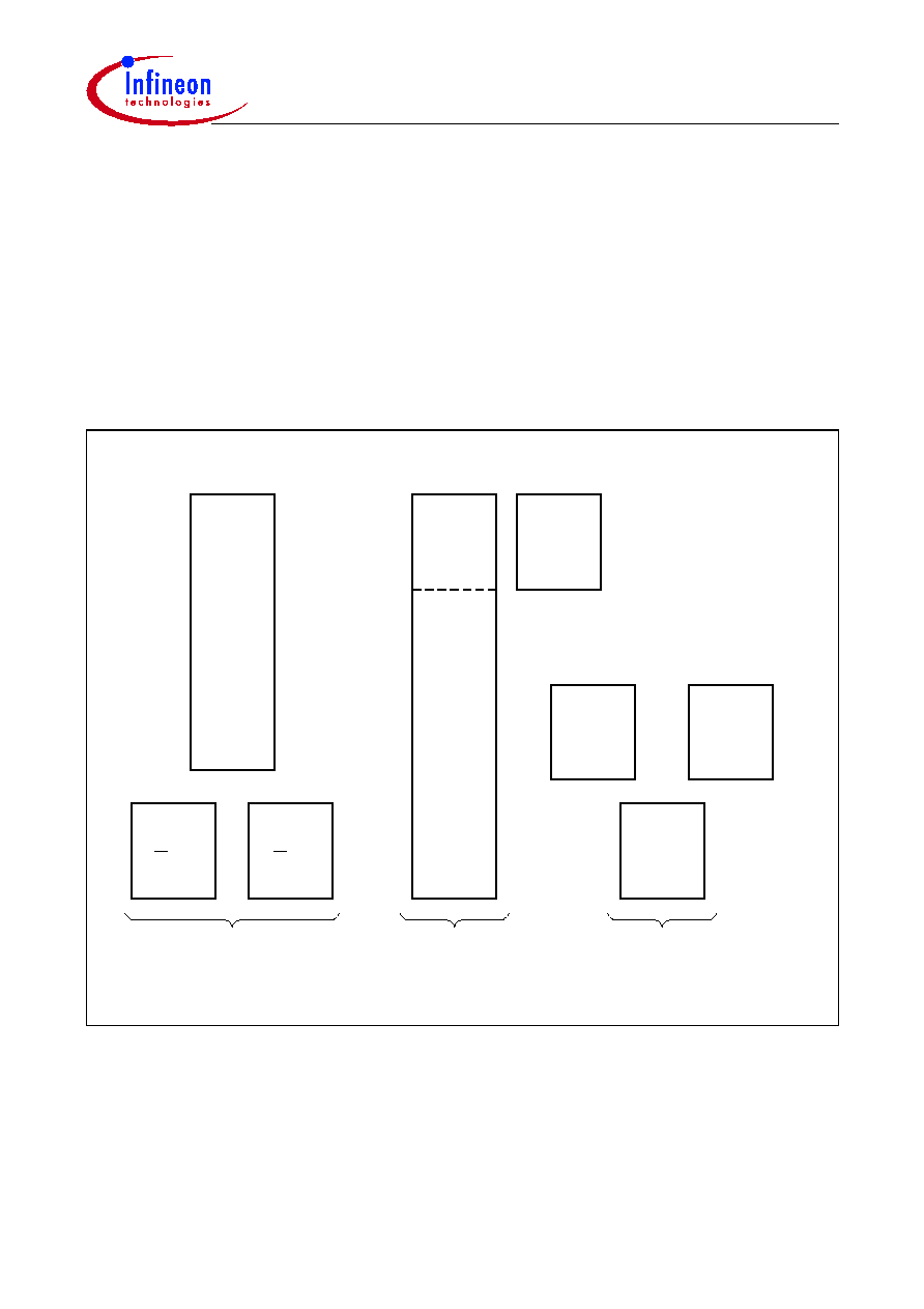
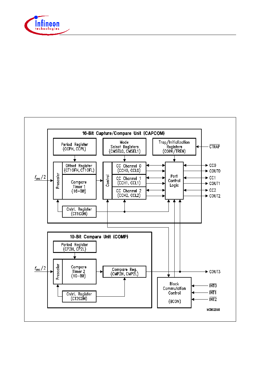
Figure 1
C504 Functional Units
MCB02589
On-Chip Emulation Support Module
Port 0
Port 1
Port 2
Port 3
RAM
256 x 8
XRAM
256 x 8
C500
T0
T1
8-Bit
USART
ROM/OTP
16 k x 8
Oscillator Watchdog
10-Bit ADC
Timer 2
10-Bit Compare Unit
16-Bit
Capture/Compare
Unit
Watchdog Timer
I/O
4-Bit Analog Inputs
I/O
8-Bit Digital I/O
8-Bit Digital I/O
4-Bit Analog Inputs
Core

C504
Data Sheet
2
2000-05
∑ Capture/compare unit for PWM signal generation and signal capturing
≠ 3-channel, 16-bit capture/compare unit
≠ 1-channel, 10-bit compare unit
∑ Full duplex serial interface (USART)
∑ 10-bit A/D Converter with 8 multiplexed inputs
∑ Twelve interrupt sources with two priority levels
∑ On-chip emulation support logic (Enhanced Hooks Technology
TM
)
∑ Programmable 15-bit Watchdog Timer
∑ Oscillator Watchdog
∑ Fast Power On Reset
∑ Power Saving Modes
≠ Idle mode
≠ Power-down mode with wake-up capability through INT0
∑ M-QFP-44 package
∑ Temperature ranges: SAB-C504
T
A
: 0 to 70
∞
C
SAF-C504
T
A
: ≠ 40 to 85
∞
C
SAK-C504
T
A
: ≠ 40 to 125
∞
C
(max. operating frequency: 24 MHz)
Ordering Information
The ordering code for Infineon Technologies microcontrollers provides an exact
reference to the required product. This ordering code indentifies:
∑ The derivative itself, i.e. its function set
∑ the specified temperature range
∑ the package and the type of delivery
For the available ordering codes for the C504, please refer to the "Product Information
Microcontrollers" which summarizes all available microcontroller variants.
Note: The ordering codes for the Mask-ROM versions are defined for each product after
verification of the respective ROM code.

C504
Data Sheet
3
2000-05
Figure 2
Logic Symbol
MCL02590
DD
V
V
SS
V
AREF
AGND
V
XTAL1
XTAL2
RESET
EA
ALE
PSEN
CTRAP
COUT3
C504
Port 0
8-Bit Digital I/O
8-Bit Digital I/O/
Port 1
4-Bit Analog Inputs
Port 2
8-Bit Digital I/O
4-Bit Analog Inputs
Port 3
8-Bit Digital I/O/

C504
Data Sheet
4
2000-05
Figure 3
Pin Configuration (top view)
EA
COUT3
P0.6 / AD6
P0.7 / AD7
P0.5 / AD5
P2.6 / A14
P2.5 / A13
PSEN
P2.7 / A15
ALE
P2.4 / A12
P2.3 / A11
XTAL2
XTAL1
CTRAP
P1.7 / COUT2
P3.2 / AN4 / INT0
P3.3 / AN5 / INT1
RESET
P1.6 / CC2
P1.5 / COUT1
11
1
6
34
39
44
16
21
22
C504-LM
MCP02532
P2.2 / A10
P2.1 / A9
V
V
DD
SS
P2.0 / A8
33
31 30 29 28 27 26 25 24 23
32
P0.4 / AD4
P3.0 / RxD
P3.4 / AN6 /
T0
P3.5 / AN7 /
T1
P3.1 /
TxD
P1.4 / CC1
V
V
AREF
GND
2 3 4 5
7 8
10
9
20
19
18
17
15
14
13
12
43
42
41
40
38
37
36
35
C504-2RM
P1.1 / AN1 / T2EX
P1.0 / AN0 / T2
P1.3 / AN3 / COUT0
P1.2 / AN2 / CC0
P0.3 / AD3
P0.2 / AD2
P0.1 / AD1
P0.0 / AD0
P3.7 / RD
P3.6 / WR / INT2
C504-2EM

C504
Data Sheet
5
2000-05
Table 1
Pin Definitions and Functions
Symbol
Pin Number
(P-MQFP-44)
I/O
1)
Function
P1.0 - P1.7 40 - 44,
1 - 3
40
41
42
43
44
1
2
3
I/O
Port 1
is an 8-bit bidirectional port. Port 1 pins can be used
for digital input/output. P1.0 - P1.3 can also be used
as analog inputs of the A/D converter. As secondary
digital functions, Port 1 contains the Timer 2 pins
and the Capture/Compare inputs/outputs. Port 1
pins are assigned to be used as analog inputs via
the register P1ANA.
The functions are assigned to the pins of Port 1 as
follows:
P1.0 / AN0 / T2
Analog input channel 0 /
input to Timer 2
P1.1 / AN1 / T2EX
Analog input channel 1 /
capture/reload trigger of Timer
2 up-down count
P1.2 / AN2 / CC0
Analog input channel 2 /
input/output of capture/
compare channel 0
P1.3 / AN3 / COUT0 Analog input channel 3 /
output of capture/compare
channel 0
P1.4 / CC1
Input/output of capture/
compare channel 1
P1.5 / COUT1
Output of capture/compare
channel 1
P1.6 / CC2
Input/output of capture/
compare channel 2
P1.7 / COUT2
Output of capture/compare
channel 2
RESET
4
I
RESET
A high level on this pin for two machine cycles while
the oscillator is running resets the device. An
internal diffused resistor to
V
SS
permits power-on
reset using only an external capacitor to
V
DD
.

C504
Data Sheet
6
2000-05
P3.0 - P3.7 5, 7 - 13
5
7
8
9
10
11
12
13
I/O
Port 3
is an 8-bit bidirectional port. P3.0 (R
◊
D) and P3.1
(T
◊
D) operate as defined for the C501. P3.2 to P3.7
contain the external interrupt inputs, timer inputs,
and four of the analog inputs of the A/D converter.
Port 3 pins are assigned to be used as analog inputs
via the bits of SFR P3ANA. P3.6/WR can be
assigned as a third interrupt input.
The functions are assigned to the pins of port 3 as
follows:
P3.0 / RxD
Receiver data input (asynch.) or
data input/output (synch.) of
serial interface
P3.1 / TxD
Transmitter data output
(asynch.) or clock output
(synch.) of serial interface
P3.2 / AN4 / INT0 Analog input channel 4 /
external interrupt 0 input /
Timer 0 gate control input
P3.3 / AN5 / INT1 Analog input channel 5 /
external interrupt 1 input /
Timer 1 gate control input
P3.4 / AN6 / T0
Analog input channel 6 / Timer 0
counter input
P3.5 / AN7 / T1
Analog input channel 7 / Timer 1
counter input
P3.6 / WR / INT2
WR control output; latches the
data byte from port 0 into the
external data memory /
external interrupt 2 input
P3.7 / RD
RD control output; enables the
external data memory
Table 1
Pin Definitions and Functions (cont'd)
Symbol
Pin Number
(P-MQFP-44)
I/O
1)
Function
C504
Data Sheet
7
2000-05
CTRAP
6
I
CCU Trap Input
With CTRAP = low, the compare outputs of the
CAPCOM unit are switched to the logic level as
defined in the COINI register (if they are enabled by
the bits in SFR TRCON). CTRAP is an input pin with
an internal pullup resistor. For power saving
reasons, the signal source which drives the CTRAP
input should be at high or floating level during
power-down mode.
XTAL2
14
≠
XTAL2
Output of the inverting oscillator amplifier.
XTAL1
15
≠
XTAL1
Input to the inverting oscillator amplifier and input to
the internal clock generator circuits.
To drive the device from an external clock source,
XTAL1 should be driven, while XTAL2 is left
unconnected. There are no requirements on the
duty cycle of the external clock signal, since the
input to the internal clocking circuitry is divided down
by a divide-by-two flip-flop. Minimum and maximum
high and low times as well as rise/fall times specified
in the AC characteristics must be observed.
P2.0 - P2.7 18-25
I/O
Port 2
is a bidirectional I/O port with internal pullup
resistors. Port 2 pins that have "1"s written to them
are pulled high by the internal pullup resistors, and
in that state can be used as inputs. As inputs, Port 2
pins being externally pulled low will source current
(
I
IL
, in the DC characteristics) because of the
internal pullup resistors. Port 2 emits the high-order
address byte during fetches from external program
memory and during accesses to external data
memory that use 16-bit addresses (MOVX @DPTR).
In this application it uses strong internal pullup
resistors when issuing "1"s. During accesses to
external data memory that use 8-bit addresses
(MOVX @Ri), Port 2 issues the contents of the P2
special function register.
Table 1
Pin Definitions and Functions (cont'd)
Symbol
Pin Number
(P-MQFP-44)
I/O
1)
Function

C504
Data Sheet
8
2000-05
PSEN
26
O
The Program Store Enable
output is a control signal that enables the external
program memory to the bus during external fetch
operations. It is activated every six oscillator periods
except during external data memory accesses.
Remains high during internal program execution.
ALE
27
O
The Address Latch Enable
output is used for latching the low-byte of the
address into external memory during normal
operation. It is activated every six oscillator periods
except during an external data memory access.
When instructions are executed from internal ROM
(EA = 1) the ALE generation can be disabled by
clearing bit EALE in SFR SYSCON.
COUT3
28
O
10-Bit compare channel output
This pin is used for the output signal of the 10-bit
Compare Timer 2 unit. COUT3 can be disabled and
set to a high or low state.
EA
29
I
External Access Enable
When held at high level, instructions are fetched
from the internal ROM (C504-2R only) when the PC
is less than 4000
H
. When held at low level, the C504
fetches all instructions from external program
memory.
For the C504-L, this pin must be tied low.
P0.0 - P0.7 37 - 30
I/O
Port 0
is an 8-bit open-drain bidirectional I/O port. Port 0
pins that have "1"s written to them float; and in that
state, can be used as high-impedance inputs. Port 0
is also the multiplexed low-order address and data
bus during accesses to external program or data
memory. In this application, it uses strong internal
pullup resistors when issuing "1" s.
Port 0 also outputs the code bytes during program
verification in the C504-2R. External pullup resistors
are required during program (ROM) verification.
V
AREF
38
≠
Reference voltage for the A/D converter.
Table 1
Pin Definitions and Functions (cont'd)
Symbol
Pin Number
(P-MQFP-44)
I/O
1)
Function

C504
Data Sheet
9
2000-05
V
AGND
39
≠
Reference ground for the A/D converter.
V
SS
16
≠
Ground (0 V)
V
DD
17
≠
Power Supply (+ 5 V)
1) I = Input,
O = Output
Table 1
Pin Definitions and Functions (cont'd)
Symbol
Pin Number
(P-MQFP-44)
I/O
1)
Function

C504
Data Sheet
10
2000-05
Figure 4
Block Diagram of the C504
MCB02591
Oscillator Watchdog
OSC & Timing
CPU
Timer 1
Timer 2
Interrupt Unit
USART
Capture/Compare Unit
A/D Converter 10-Bit
Timer 0
S & H
MUX
XRAM
256 x 8
RAM
ROM/OTP
16 k x 8
Port 0
Port 1
Port 2
Port 3
Port 0
Port 1
Port 2
Port 3
XTAL2
XTAL1
V
DD
SS
V
RESET
ALE
PSEN
EA
COUT3
CTRAP
V
AGND
AREF
V
8-Bit Digital I/O
4-Bit Analog Inputs
8-Bit Digital I/O
8-Bit Digital I/O
4-Bit Analog Inputs
8-Bit Digital I/O
Support
Emulation
Logic
256 x 8
C504
Data Sheet
11
2000-05
CPU
The C504 is efficient both as a controller and as an arithmetic processor. It has extensive
facilities for binary and BCD arithmetic and excels in its bit-handling capabilities. Efficient
use of program memory results from an instruction set consisting of 44% one-byte, 41%
two-byte, and 15% three-byte instructions. With a 12 MHz crystal, 58% of the instructions
are executed in 1.0
µ
s
(
24 MHz: 500 ns, 40 MHz: 300 ns).
Special Function Register PSW (Address D0
H
)
Reset Value: 00
H
Bit
Function
CY
Carry Flag
Used by arithmetic instructions.
AC
Auxiliary Carry Flag
Used by instructions which execute BCD operations.
F0
General Purpose Flag 0
RS1
RS0
Register Bank Select Control bits
These bits are used to select one of the four register banks.
OV
Overflow Flag
Used by arithmetic instruction.
F1
General Purpose Flag 1
P
Parity Flag
Set/cleared by hardware after each instruction to indicate an odd/
even number of "one" bits in the accumulator.
CY
AC
F0
RS1
RS0
OV
F1
P
D0
H
PSW
D7
H
D6
H
D5
H
D4
H
D3
H
D2
H
D1
H
D0
H
Bit No.
MSB
LSB
RS1
RS0
Function
0
0
Bank 0 selected, data address 00
H
-07
H
0
1
Bank 1 selected, data address 08
H
-0F
H
1
0
Bank 2 selected, data address 10
H
-17
H
1
1
Bank 3 selected, data address 18
H
-1F
H
C504
Data Sheet
12
2000-05
Memory Organization
The C504 CPU manipulates operands in the following four address spaces:
≠ up to 64 Kbyte of program memory:
16K ROM for C504-2R
16K OTP for C504-2E
≠ up to 64 Kbyte of external data memory
≠ 256 bytes of internal data memory
≠ 256 bytes of internal XRAM data memory
≠ a 128 byte special function register area
Figure 5 illustrates the memory address spaces of the C504.
Figure 5
C504 Memory Map
MCD02592
00H
H
7F
0000 H
3FFFH
External
FFFF H
H
4000
(EA = 0)
(EA = 1)
"Code Space"
"Data Space"
"Internal Data Space"
H
0000
H
FFFF
External
FF00 H
FEFFH
Internal
XRAM
RAM
Internal
Internal
External
Internal
RAM
FFH
H
80
Function
Special
Register
Direct
Address
80H
H
FF
Address
Indirect

C504
Data Sheet
13
2000-05
Reset and System Clock Operation
The reset input is an active high input. An internal Schmitt trigger is used at the input for
noise rejection. Since the reset is synchronized internally, the RESET pin must be held
high for at least two machine cycles (24 oscillator periods) while the oscillator is running.
During reset, pins ALE and PSEN are configured as inputs and should not be stimulated
externally. (An external stimulation at these lines during reset activates several test
modes which are reserved for test purposes. This, in turn, may cause unpredictable
output operations at several port pins).
At the reset pin, a pulldown resistor is internally connected to
V
SS
to allow a power-up
reset with an external capacitor only. An automatic reset can be obtained when
V
DD
is
applied by connecting the reset pin to
V
DD
via a capacitor. After
V
DD
has been turned on,
the capacitor must hold the voltage level at the reset pin for a specific time to effect a
complete reset.
The time required for a reset operation is the oscillator start-up time and the time for
2 machine cycles, which must be at least 10 - 20 ms, under normal conditions. This
requirement is typically met using a capacitor of 4.7 to 10
µ
F. The same considerations
apply if the reset signal is generated externally (Figure 6b). In each case, it must be
assured that the oscillator has started up properly and that at least two machine cycles
have passed before the reset signal goes inactive.
Figure 6 shows the possible reset circuitries.
Figure 6
Reset Circuitries
a)
+
b)
+
C504
RESET
c)
&
MCS03352
C504
C504
RESET
RESET

C504
Data Sheet
14
2000-05
Figure 7 shows the recommended oscillator circuit for the C504, while Figure 8 shows
the circuit for using an external clock source.
Figure 7
Recommended Oscillator Circuit
Figure 8
External Clock Source
MCS03353
C
3.5 - 40
MHz
XTAL2
XTAL1
C = 20 pF 10 pF for crystal operation
C504
C
MCS03355
XTAL1
XTAL2
N.C.
V
DD
C504
External
Clock
Signal

C504
Data Sheet
15
2000-05
Enhanced Hooks Emulation Concept
The Enhanced Hooks Emulation Concept of the C500 microcontroller family is a new,
innovative way to control the execution of C500 MCUs and to gain extensive information
on the internal operation of the controllers. Emulation of on-chip ROM based programs
is possible, too.
Each production chip has built-in logic for the support of the Enhanced Hooks Emulation
Concept. Therefore, no costly bond-out chips are necessary for emulation. This also
ensure that emulation and production chips are identical.
The Enhanced Hooks Technology
TM
, which requires embedded logic in the C500 allows
the C500 together with an EH-IC to function similar to a bond-out chip. This simplifies the
design and reduces costs of an ICE-system. ICE-systems using an EH-IC and a
compatible C500 are able to emulate all operating modes of the different versions of the
C500. This includes emulation of ROM, ROM with code rollover and ROMless modes of
operation. It is also able to operate in single step mode and to read the SFRs after a
break.
Figure 9
Basic C500 MCU Enhanced Hooks Concept Configuration
Port 0, Port 2 and some of the control lines of the C500 based MCU are used by
Enhanced Hooks Emulation Concept to control the operation of the device during
emulation and to transfer informations about the program execution and data transfer
between the external emulation hardware (ICE-system) and the C500 MCU.
MCS02647
SYSCON
PCON
TCON
RESET
EA
PSEN
ALE
Port 0
Port 2
I/O Ports
Optional
Port 3
Port 1
C500
MCU
Interface Circuit
Enhanced Hooks
RPort 0
RPort 2
RTCON
RPCON
RSYSCON
TEA
TALE TPSEN
EH-IC
Target System Interface
ICE-System Interface
to Emulation Hardware

C504
Data Sheet
16
2000-05
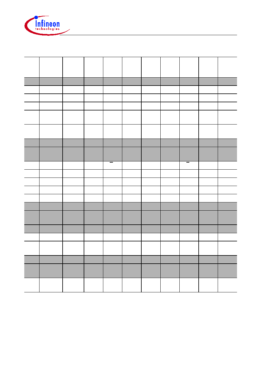
Special Function Registers
All registers, except the program counter and the four general purpose register banks,
reside in the special function register area.
The 63 special function registers (SFR) include pointers and registers that provide an
interface between the CPU and the other on-chip peripherals. All SFRs with addresses
where address bits 0-2 are 0 (e.g. 80
H
, 88
H
, 90
H
, 98
H
, ..., F0
H
, F8
H
) are bit-addressable.
The SFRs of the C504 are listed in Table 2 and Table 3. In Table 2, they are organized
in groups which refer to the functional blocks of the C504. Table 3 illustrates the contents
of the SFRs in numeric order of their addresses.

C504
Data Sheet
17
2000-05
Table 2
Special Function Registers - Functional Blocks
Block
Symbol Name
Addr.
Contents
after
Reset
CPU
ACC
B
DPH
DPL
PSW
SP
SYSCON
Accumulator
B-Register
Data Pointer, High Byte
Data Pointer, Low Byte
Program Status Word Register
Stack Pointer
System Control Register
E0
H
1)
F0
H
1)
83
H
82
H
D0
H
1)
81
H
B1
H
00
H
00
H
00
H
00
H
00
H
07
H
XX10XXX0
B
3)
Interrupt
System
IEN0
IEN1
CCIE
2)
IP0
IP1
ITCON
Interrupt Enable Register 0
Interrupt Enable Register 1
Capture/Compare Interrupt Enable Reg.
Interrupt Priority Register 0
Interrupt Priority Register 1
Interrupt Trigger Condition Register
A8
H
1)
A9
H
D6
H
B8
H
1)
B9
H
9A
H
0X000000
B
3)
XX000000
B
3)
00
H
XX000000
B
3)
XX000000
B
3)
00101010
B
Ports
P0
P1
P1ANA
2)
P2
P3
P3ANA
2)
Port 0
Port 1
Port 1 Analog Input Selection Register
Port 2
Port 3
Port 3 Analog Input Selection Register
80
H
1)
90
H
1)
90
H
1) 4)
A0
H
1)
B0
H
1)
B0
H
1) 4)
FF
H
FF
H
XXXX1111
B
3)
FF
H
FF
H
XX1111XX
B
3)
A/D-
Converter
ADCON0
ADCON1
ADDATH
ADDATL
P1ANA
2)
P3ANA
2)
A/D Converter Control Register 0
A/D Converter Control Register 1
A/D Converter Data Register High Byte
A/D Converter Data Register Low Byte
Port 1 Analog Input Selection Register
Port 3 Analog Input Selection Register
D8
H
1)
DC
H
D9
H
DA
H
90
H
1) 4)
B0
H
1) 4)
XX000000
B
3)
01XXX000
B
3)
00
H
00XXXXXX
B
3)
XXXX1111
B
3)
XX1111XX
B
3)
Serial
Channels
PCON
2)
SBUF
SCON
Power Control Register
Serial Channel Buffer Register
Serial Channel Control Register
87
H
99
H
98
H
1)
000X0000
B
XX
H
3)
00
H
Timer 0/
Timer 1
TCON
TH0
TH1
TL0
TL1
TMOD
Timer 0/1 Control Register
Timer 0, High Byte
Timer 1, High Byte
Timer 0, Low Byte
Timer 1, Low Byte
Timer Mode Register
88
H
1)
8C
H
8D
H
8A
H
8B
H
89
H
00
H
00
H
00
H
00
H
00
H
00
H
1) Bit-addressable special function registers
2) This special function register is listed repeatedly since some bits of it also belong to other functional blocks.
3) X means that the value is undefined and the location is reserved
4) SFR is located in the mapped SFR area. For accessing this SFR, bit RMAP in SFR SYSCON must be set.

C504
Data Sheet
18
2000-05
Timer 2
T2CON
T2MOD
RC2H
RC2L
TH2
TL2
Timer 2 Control Register
Timer 2 Mode Register
Timer 2 Reload Capture Register, High Byte
Timer 2 Reload Capture Register, Low Byte
Timer 2 High Byte
Timer 2 Low Byte
C8
H
1)
C9
H
CB
H
CA
H
CD
H
CC
H
00
H
XXXXXXX0
B
3)
00
H
00
H
00
H
00
H
Capture /
Compare
Unit
CT1CON
CCPL
CCPH
CT1OFL
CT1OFH
CMSEL0
CMSEL1
COINI
TRCON
CCL0
CCH0
CCL1
CCH1
CCL2
CCH2
CCIR
CCIE
2)
CT2CON
CP2L
CP2H
CMP2L
CMP2H
BCON
Compare timer 1 control register
Compare timer 1 period register, low byte
Compare timer 1 period register, high byte
Compare timer 1 offset register, low byte
Compare timer 1 offset register, high byte
Capture/compare mode select register 0
Capture/compare mode select register 1
Compare output initialization register
Trap enable control register
Capture/compare register 0, low byte
Capture/compare register 0, high byte
Capture/compare register 1, low byte
Capture/compare register 1, high byte
Capture/compare register 2, low byte
Capture/compare register 2, high byte
Capture/compare interrupt request flag reg.
Capture/compare interrupt enable register
Compare timer 2 control register
Compare timer 2 period register, low byte
Compare timer 2 period register, high byte
Compare timer 2 compare register, low byte
Compare timer 2 compare register, high byte
Block commutation control register
E1
H
DE
H
DF
H
E6
H
E7
H
E3
H
E4
H
E2
H
CF
H
C2
H
C3
H
C4
H
C5
H
C6
H
C7
H
E5
H
D6
H
C1
H
D2
H
D3
H
D4
H
D5
H
D7
H
00010000
B
00
H
00
H
00
H
00
H
00
H
00
H
FF
H
00
H
00
H
00
H
00
H
00
H
00
H
00
H
00
H
00
H
00010000
B
00
H
XXXXXX00
B
3)
00
H
XXXXXX00
B
3)
00
H
Watchdog
Timer
WDCON
WDTREL
Watchdog Timer Control Register
Watchdog Timer Reload Register
C0
H
1)
86
H
XXXX0000
B
3)
00
H
Power
Saving
Mode
PCON
2)
PCON1
Power Control Register
Power Control Register 1
87
H
88
H
1) 4)
000X0000
B
3)
0XXXXXXX
B
3)
1) Bit-addressable special function registers
2) This special function register is listed repeatedly since some bits of it also belong to other functional blocks.
3) X means that the value is undefined and the location is reserved
4) SFR is located in the mapped SFR area. For accessing this SFR, bit RMAP in SFR SYSCON must be set.
Table 2
Special Function Registers - Functional Blocks (cont'd)
Block
Symbol Name
Addr.
Contents
after
Reset
C504
Data Sheet
19
2000-05
Table 3
Contents of the SFRs, SFRs in Numeric Order of their Addresses
Addr
Register Content
after
Reset
1)
Bit 7
Bit 6
Bit 5
Bit 4
Bit 3
Bit 2
Bit 1
Bit 0
80
H
2)
P0
FF
H
.7
.6
.5
.4
.3
.2
.1
.0
81
H
SP
07
H
.7
.6
.5
.4
.3
.2
.1
.0
82
H
DPL
00
H
.7
.6
.5
.4
.3
.2
.1
.0
83
H
DPH
00
H
.7
.6
.5
.4
.3
.2
.1
.0
86
H
WDTREL 00
H
WDT
PSEL
.6
.5
.4
.3
.2
.1
.0
87
H
PCON
000X-
0000
B
SMOD PDS
IDLS
≠
GF1
GF0
PDE
IDLE
88
H
2)
TCON
00
H
TF1
TR1
TF0
TR0
IE1
IT1
IE0
IT0
88
H
1)3)
PCON1
0XXX-
XXXX
B
EWPD ≠
≠
≠
≠
≠
≠
≠
89
H
TMOD
00
H
GATE
C/T
M1
M0
GATE
C/T
M1
M0
8A
H
TL0
00
H
.7
.6
.5
.4
.3
.2
.1
.0
8B
H
TL1
00
H
.7
.6
.5
.4
.3
.2
.1
.0
8C
H
TH0
00
H
.7
.6
.5
.4
.3
.2
.1
.0
8D
H
TH1
00
H
.7
.6
.5
.4
.3
.2
.1
.0
90
H
2)
P1
FF
H
.7
.6
.5
.4
.3
.2
T2EX
T2
90
H
2)3)
P1ANA
XXXX-
1111
B
≠
≠
≠
≠
EAN3
EAN2
EAN1
EAN0
98
H
2)
SCON
00
H
SM0
SM1
SM2
REN
TB8
RB8
TI
RI
99
H
SBUF
XX
H
.7
.6
.5
.4
.3
.2
.1
.0
9A
H
ITCON
0010-
1010
B
IT2
IE2
I2ETF
I2ETR
I1ETF
I1ETR
I0ETF
I0ETR
A0
H
2)
P2
FF
H
.7
.6
.5
.4
.3
.2
.1
.0
A8
H
2)
IEN0
0X00-
0000
B
EA
≠
ET2
ES
ET1
EX1
ET0
EX0
A9
H
IEN1
XX00-
0000
B
≠
≠
ECT1
ECCM
ECT2
ECEM
EX2
EADC
1) X means that the value is undefined and the location is reserved
2) Bit-addressable special function registers
3) SFR is located in the mapped SFR area. For accessing this SFR, bit RMAP in SFR SYSCON must be set.

C504
Data Sheet
20
2000-05
B0
H
2)
P3
FF
H
RD
WR
T1
T0
INT1
INT0
TxD
RxD
B0
H
2)3)
P3ANA
XX11-
11XX
B
≠
≠
EAN7
EAN6
EAN5
EAN4
≠
≠
B1
H
SYSCON XX10-
XXX0
B
≠
≠
EALE
RMAP
≠
≠
≠
XMAP
B8
H
2)
IP0
XX00-
0000
B
≠
≠
PT2
PS
PT1
PX1
PT0
PX0
B9
H
IP1
XX00-
0000
B
≠
≠
PCT1
PCCM
PCT2
PCEM
PX2
PADC
C0
H
2)
WDCON XXXX-
0000
B
≠
≠
≠
≠
OWDS WDTS
WDT
SWDT
C1
H
CT2CON 0001-
0000
B
CT2P
ECT2O STE2
CT2
RES
CT2R
CLK2
CLK1
CLK0
C2
H
CCL0
00
H
.7
.6
.5
.4
.3
.2
.1
.0
C3
H
CCH0
00
H
.7
.6
.5
.4
.3
.2
.1
.0
C4
H
CCL1
00
H
.7
.6
.5
.4
.3
.2
.1
.0
C5
H
CCH1
00
H
.7
.6
.5
.4
.3
.2
.1
.0
C6
H
CCL2
00
H
.7
.6
.5
.4
.3
.2
.1
.0
C7
H
CCH2
00
H
.7
.6
.5
.4
.3
.2
.1
.0
C8
H
2)
T2CON
00
H
TF2
EXF2
RCLK
TCLK
EXEN2 TR2
C/T2
CP/
RL2
C9
H
T2MOD
XXXX-
XXX0
B
≠
≠
≠
≠
≠
≠
≠
DCEN
CA
H
RC2L
00
H
.7
.6
.5
.4
.3
.2
.1
.0
CB
H
RC2H
00
H
.7
.6
.5
.4
.3
.2
.1
.0
CC
H
TL2
00
H
.7
.6
.5
.4
.3
.2
.1
.0
CD
H
TH2
00
H
.7
.6
.5
.4
.3
.2
.1
.0
CF
H
TRCON
00
H
TRPEN TRF
TREN5 TREN4 TREN3 TREN2 TREN1 TREN0
1) X means that the value is undefined and the location is reserved
2) Bit-addressable special function registers
3) SFR is located in the mapped SFR area. For accessing this SFR, bit RMAP in SFR SYSCON must be set.
Table 3
Contents of the SFRs, SFRs in Numeric Order of their Addresses (cont'd)
Addr
Register Content
after
Reset
1)
Bit 7
Bit 6
Bit 5
Bit 4
Bit 3
Bit 2
Bit 1
Bit 0
C504
Data Sheet
21
2000-05
D0
H
2)
PSW
00
H
CY
AC
F0
RS1
RS0
OV
F1
P
D2
H
CP2L
00
H
.7
.6
.5
.4
.3
.2
.1
.0
D3
H
CP2H
XXXX.
XX00
B
≠
≠
≠
≠
≠
≠
.1
.0
D4
H
CMP2L
00
H
.7
.6
.5
.4
.3
.2
.1
.0
D5
H
CMP2H
XXXX.
XX00
B
≠
≠
≠
≠
≠
≠
.1
.0
D6
H
CCIE
00
H
ECTP
ECTC
CC2
FEN
CC2
REN
CC1
FEN
CC1
REN
CC0
FEN
CC0
REN
D7
H
BCON
00
H
BCMP
BCEM
PWM1 PWM0 EBCE
BCERR BCEN
BCM1
BCM0
D8
H
2)
ADCON0 XX00-
0000
B
≠
≠
IADC
BSY
ADM
MX2
MX1
MX0
D9
H
ADDATH 00
H
.9
.8
.7
.6
.5
.4
.3
.2
DA
H
ADDATL 00XX-
XXXX
B
.1
.0
≠
≠
≠
≠
≠
≠
DC
H
ADCON1 01XX-
X000
B
ADCL1 ADCL0 ≠
≠
≠
MX2
MX1
MX0
DE
H
CCPL
00
H
.7
.6
.5
.4
.3
.2
.1
.0
DF
H
CCPH
00
H
.7
.6
.5
.4
.3
.2
.1
.0
E0
H
2)
ACC
00
H
.7
.6
.5
.4
.3
.2
.1
.0
E1
H
CT1CON 0001-
0000
B
CTM
ETRP
STE1
CT1
RES
CT1R
CLK2
CLK1
CLK0
E2
H
COINI
FF
H
COUT
3I
COUTX
I
COUT
2I
CC2I
COUT
1I
CC1I
COUT
0I
CC0I
E3
H
CMSEL0 00
H
CMSEL
13
CMSEL
12
CMSEL
11
CMSEL
10
CMSEL
03
CMSEL
02
CMSEL
01
CMSEL
00
E4
H
CMSEL1 00
H
0
0
0
0
CMSEL
23
CMSEL
22
CMSEL
21
CMSEL
20
E5
H
CCIR
00
H
CT1FP CT1FC CC2F
CC2R
CC1F
CC1R
CC0F
CC0R
E6
H
CT1OFL 00
H
.7
.6
.5
.4
.3
.2
.1
.0
E7
H
CT1OFH 00
H
.7
.6
.5
.4
.3
.2
.1
.0
F0
H
2)
B
00
H
.7
.6
.5
.4
.3
.2
.1
.0
1) X means that the value is undefined and the location is reserved
2) Bit-addressable special function registers
Table 3
Contents of the SFRs, SFRs in Numeric Order of their Addresses (cont'd)
Addr
Register Content
after
Reset
1)
Bit 7
Bit 6
Bit 5
Bit 4
Bit 3
Bit 2
Bit 1
Bit 0

C504
Data Sheet
22
2000-05
Timer/Counter 0 and 1
Timer/Counter 0 and 1 can be used in four operating modes as listed in Table 4.
In the "timer" function (C/
T
= `0'), the register is incremented every machine cycle.
Therefore the count rate is
f
OSC
/12.
In the "counter" function the register is incremented in response to a 1-to-0 transition at
its corresponding external input pin (P3.4/T0, P3.5/T1). Since it takes two machine
cycles to detect a falling edge the max. count rate is
f
OSC
/24. External inputs INT0 and
INT1
(P3.2, P3.3) can be programmed to function as a gate to facilitate pulse width
measurements. Figure 10 illustrates the input clock logic.
Figure 10
Timer/Counter 0 and 1 Input Clock Logic
Table 4
Timer/Counter 0 and 1 Operating Modes
Mode Description
TMOD
Input Clock
Gate C/
T
M1 M0 internal
external
(max.)
0
8-bit timer/counter with a
divide-by-32 prescaler
X
X
0
0
f
OSC
/12
◊
32
f
OSC
/24
◊
32
1
16-bit timer/counter
X
X
1
1
f
OSC
/12
f
OSC
/24
2
8-bit timer/counter with
8-bit auto-reload
X
X
0
0
f
OSC
/12
f
OSC
/24
3
Timer/counter 0 used as one
8-bit timer/counter and one
8-bit timer
Timer 1 stops
X
X
1
1
f
OSC
/12
f
OSC
/24
12
f
OSC
/12
MCS01768
OSC
f
C/T
TMOD
0
Control
Timer 0/1
Input Clock
TCON
TR 0/1
Gate
TMOD
&
=1
1
P3.4/T0
P3.5/T1
max
P3.2/INT0
P3.3/INT1
OSC
/24
f
1
˜
_
<
C504
Data Sheet
23
2000-05
Timer/Counter 2
Timer 2 is a 16-bit Timer/Counter with an up/down count feature. It can operate either as
a timer or as an event counter. This is selected by bit C/
T2
of SFR T2CON. It has three
operating modes as shown in Table 5.
Note:
=
falling edge
Table 5
Timer/Counter 2 Operating Modes
Mode
T2CON
T2MOD
DCEN
T2CON
EXEN
P1.1/
T2EX
Remarks
Input Clock
R
◊
CLK
or
T
◊
CLK
CP/
RL2
TR2
internal external
(P1.0/T2)
16-bit
Auto-
reload
0
0
0
0
0
0
0
0
1
1
1
1
0
0
1
1
0
1
X
X
X
0
1
reload upon
overflow
reload trigger
(falling edge)
Down counting
Up counting
f
OSC
/12
max
f
OSC
/24
16-bit
Cap-
ture
0
0
1
1
1
1
X
X
0
1
X
16 bit Timer/
Counter (only
up-counting)
capture TH2,
TL2
RC2H,
RC2L
f
OSC
/12
max
f
OSC
/24
Baud
Rate
Gene-
rator
1
1
X
X
1
1
X
X
0
1
X
no overflow
interrupt
request (TF2)
extra external
interrupt
("Timer 2")
f
OSC
/2
max
f
OSC
/24
off
X
X
0
X
X
X
Timer 2 stops
≠
≠
C504
Data Sheet
24
2000-05
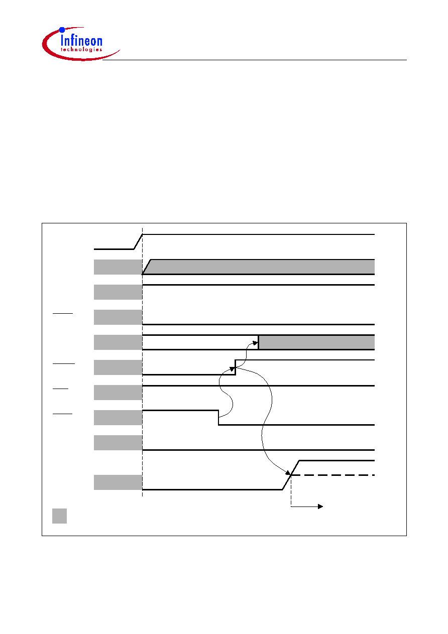
Capture/Compare Unit
The Capture/Compare Unit (CCU) of the C504 consists of a 16-bit 3-channel capture/
compare unit (CAPCOM) and a 10-bit 1-channel compare unit (COMP). In compare
mode, the CAPCOM unit provides two output signals per channel, which can have
inverted signal polarity and non-overlapping pulse transitions. The COMP unit can
generate a single PWM output signal and is further used to modulate the CAPCOM
output signals. In capture mode, the value of the Compare Timer 1 is stored in the
capture registers if a signal transition occurs at the pins CCx. Figure 11 shows the block
diagram of the CCU.
Figure 11
Block Diagram of the CCU

C504
Data Sheet
25
2000-05
The Compare Timers 1 and 2 are free running, processor clock coupled 16-bit / 10-bit
timers; each of which has a count rate with a maximum of
f
OSC
/2 up to
f
OSC
/256. The
compare timer operations with its possible compare output signal waveforms are shown
in Figure 12.
Figure 12
Basic Operating Modes of the CAPCOM Unit
Compare Timer 1 can be programmed for both operating modes while Compare Timer 2
works only in operating mode 0 with one output signal of selectable polarity at the pin
COUT3.
Period
Value
Value
Compare
0000
H
CC
COUT
Value
Compare
Value
Period
Offset
OFF
t
Value
Compare
0000
H
Value
Period
Compare
Value
Offset
Value
Period
OFF
t
COINI=0
COINI=1
OFF
t
: Interrupts can be generated
MCT03356
Compare Timer 1 in Operating Mode 0
a) Standard PWM (Edge Aligned)
Compare Timer 1 in Operating Mode 1
b) Standard PWM (Single Edge Aligned)
with programmable dead time ( )
OFF
t
Symetrical PWM (Center Aligned)
c)
with programmable dead time ( )
Symetrical PWM (Center Aligned)
d)
OFF
t
CC
COUT
COINI=0
COINI=1
CC
COUT
CC
COUT
C504
Data Sheet
26
2000-05
Serial Interface (USART)
The serial port is full duplex and can operate in four modes (one synchronous mode,
three asynchronous modes) as illustrated in Table 6. The possible baud rates can be
calculated using the formulas given in Table 6.
Figure 13
Baud Rate Generation for the Serial Interface
Table 6
USART Operating Modes
Mode
SCON
Baud Rate
Description
SM0
SM1
0
0
0
f
OSC
/12
Serial data enters and exits through
R
◊
D. T
◊
D outputs the shift clock. 8-bit
are transmitted/received (LSB first)
1
0
1
Timer 1/2 overflow rate 8-bit UART
10 bits are transmitted (through T
◊
D)
or received (R
◊
D)
2
1
0
f
OSC
/32 or
f
OSC
/64
9-bit UART
11 bits are transmitted (T
◊
D) or
received (R
◊
D)
3
1
1
Timer 1/2 overflow rate 9-bit UART
Like mode 2 except the variable baud
rate
2
SM0 / SM1
PCON.7
(SMOD)
(RCLK, TCLK)
T2CON
Timer 1
Overflow
Phase 2
CLK
(= /2)
f
OSC
Timer 2
Overflow
Mode 1, 3
Mode 2
0
0
1
1
MCB02414
Baud
Rate
Clock

C504
Data Sheet
27
2000-05
The possible baud rates can be calculated using the formulas given in Table 7.
Table 7
Formulas for Calculating Baud Rates
Source of
Baud Rate
Operating Mode
Baud Rate
Oscillator
0
2
f
OSC
/12
(2
SMOD
◊
f
OSC
)/64
Timer 1
(16-bit timer)
(8-bit timer with
8-bit auto-reload)
1, 3
1, 3
(2
SMOD
◊
timer 1 overflow rate)/32
(2
SMOD
◊
f
OSC
)/(32
◊
12
◊
(256-TH1))
Timer 2
1, 3
f
OSC
/(32
◊
(65536-(RC2H, RC2L))

C504
Data Sheet
28
2000-05
10-Bit A/D Converter
The C504 has a high performance 8-channel 10-bit A/D converter using successive
approximation technique for the conversion of analog input voltages. Figure 14 shows
the block diagram of the A/D Converter.
Figure 14
A/D Converter Block Diagram
ADDATL
ADDATH
Shaded bit locations are not used in ADC-functions.
AREF
AGND
V
V
OSC
f
/2
˜ 32, 16, 8, 4
Prescaler
Clock
Port 1/3
Conversion
Write to
ADDATL
MCB02616
Bus
Internal
Continuous
Single/
A/D Converter
IN
Input Clock
Conversion Clock
f
ADC
f
MUX
S & H
Mode
LSB
.8
Start of
MSB
.1
.6
.7
.4
.5
.2
.3
(D9 )
H
-
-
-
-
-
-
H
(DA )
IEN1 (A9 )
ADCON0 (D8 )
ADCL1
ADCON1 (DC )
P3ANA (B0 )
P1ANA (90 )
-
-
-
-
H
BSY
-
IADC
H
ADM
MX2
EAN6
ADCL0
H
-
-
EAN7
H
-
-
EAN5
-
-
MX2
EAN4
EAN3
-
EAN2
MX1
MX0
MX1
-
MX0
-
EAN0
EAN1
ECCM
-
H
ECT1
ECT2 ECEM
EADC
EX2
Bus
Internal
C504
Data Sheet
29
2000-05
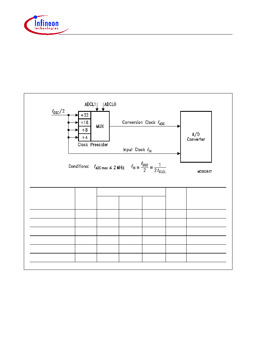
The A/D Converter uses two clock signals for operation: the conversion clock
f
ADC
(= 1/
t
ADC
) and the input clock
f
IN
(= 1/
t
IN
). Both clock signals are derived from the C504 system
clock
f
OSC
which is applied at the XTAL pins. The duration of an A/D conversion is a
multiple of the period of the
f
IN
clock signal. The table in Figure 15 shows the prescaler
ratios and the resulting A/D conversion times which must be selected for typical system
clock rates.
Figure 15
A/D Converter Clock Selection
The analog inputs are located at Port 1 and Port 3 (4 lines on each port). The
corresponding Port 1 and Port 3 pins have a port structure, which allows the pins to be
used either as digital I/Os or analog inputs. The analog input function of these mixed
digital/analog port lines is selected via the registers P1ANA and P3ANA.
MCU System Clock
Rate (
f
OSC
)
f
IN
[MHz]
Prescaler
f
ADC
[MHz]
A/D
Conversion
Time [
µ
s]
Ratio
ADCL1
ADCL0
3.5 MHz
1.75
˜
4
0
0
.438
48
◊
t
IN
= 27.4
12 MHz
6
˜
4
0
0
1.5
48
◊
t
IN
= 8
16 MHz
8
˜
4
0
0
2
48
◊
t
IN
= 6
24 MHz
12
˜
8
0
1
1.5
96
◊
t
IN
= 8
32 MHz
16
˜
8
0
1
2
96
◊
t
IN
= 6
40 MHz
20
˜
16
1
0
1.25
192
◊
t
IN
= 9.6

C504
Data Sheet
30
2000-05
Interrupt System
The C504 provides 12 interrupt sources with two priority levels. Figures 16 and 17 give
a general overview of the interrupt sources and illustrate the interrupt request and control
flags.
Figure 16
Interrupt Request Sources (Part 1)

C504
Data Sheet
31
2000-05
Figure 17
Interrupt Request Sources (Part 2)
MCB02596
ITCON.7
IT2
P3.6/WR/INT2
ITCON.4
ITCON.5
1
EX2
IE2
IEN1.1
ITCON.6
004B H
Low Priority
High Priority
IP1.1
PX2
CC0R
CC0REN
CCIE0.0
1
CCIR.0
CCIR.1
CCIE0.1
CC0FEN
CC0F
CC1F
CC1FEN
CCIE0.3
CCIR.3
CCIR.2
CCIE0.2
CC1REN
CC1R
CC2F
CC2FEN
CCIE0.5
CCIR.5
CCIR.4
CCIE0.4
CC2REN
CC2R
PCCM
IP1.4
H
0063
IEN1.4
ECCM
CCIR.7
CCIE.7
CT1FP
ECTP
ECTC
CT1FC
CCIE.6
CCIR.6
1
ECT1
IEN1.5
006B H
IP1.5
PCT1
PCT2
IP1.3
H
005B
IEN1.3
ECT2
CT2P
CT2CON.7
PCEM
IP1.2
H
0053
IEN1.2
ECEM
1
BCON.3
BCERR
EBCE
ETRP
TRF
CT1CON.6
TRCON.6
BCON.4
EA
P1.2/AN2/CC0
P1.4/CC1
P1.6/CC2
Capture/Compare Match Interrupt
Compare Timer 1
Interrupt
Interrupt
Compare Timer 2
Interrupt
CCU Emergency
Bit addressable
Request Flag is
cleared by hardware
IEN0.7
_
<
<
_
<
_
_
<
C504
Data Sheet
32
2000-05
A low-priority interrupt can itself be interrupted by a high-priority interrupt, but not by
another low-priority interrupt. A high-priority interrupt cannot be interrupted by any other
interrupt sources.
If two requests of different priority level are received simultaneously, the request of
higher priority is serviced. If requests of the same priority are received simultaneously,
an internal polling sequence determines which request is serviced. Thus within each
priority level there is a second priority structure determined by the polling sequence as
shown in Table 9.
Table 8
Interrupt Vector Addresses
Request Flags
Interrupt Source
Vector Address
IE0
TF0
IE1
TF1
RI + TI
TF2 + EXF2
IADC
IE2
TRF, BCERR
CT2P
CC0F-CC2F, CC0R-CC2R
CT1FP, CT1FC
≠
External interrupt 0
Timer 0 interrupt
External interrupt 1
Timer 1 interrupt
Serial port interrupt
Timer 2 interrupt
A/D converter interrupt
External interrupt 2
CAPCOM emergency interrupt
Compare timer 2 interrupt
Capture/compare match interrupt
Compare timer 1 interrupt
Power-down interrupt
0003
H
000B
H
0013
H
001B
H
0023
H
002B
H
0043
H
004B
H
0053
H
005B
H
0063
H
006B
H
007B
H
Table 9
Interrupt Source Structure
Interrupt Source
Priority
External Interrupt 0
Timer 0 Interrupt
External Interrupt 1
Timer 1 Interrupt
Serial Channel
Timer 2 Interrupt
A/D Converter
External Interrupt 2
CCU Emergency Interrupt
Compare Timer 2 Interrupt
Capture/Compare Match Interrupt
Compare Timer 1 Interrupt
High
Low
High Priority
Low Priority

C504
Data Sheet
33
2000-05
Fail Save Mechanisms
The C504 offers enhanced fail save mechanisms, which allow an automatic recovery
from software or hardware failure.
≠ a programmable 15-bit Watchdog Timer
≠ Oscillator Watchdog
Programmable Watchdog Timer
The Watchdog Timer in the C504 is a 15-bit timer, which is incremented by a count rate
of either
f
CYCLE
/2 or
f
CYCLE
/32 (
f
CYCLE
=
f
OSC
/12). Only the upper 7 bits of the 15-bit
watchdog timer count value can be programmed. Figure 18 shows the block diagram of
the programmable Watchdog Timer.
Figure 18
Block Diagram of the Programmable Watchdog Timer
The Watchdog Timer can be started by software (bit SWDT in SFR WDCON), but it
cannot be stopped during active mode of the device. If the software fails to refresh the
running Watchdog Timer, an internal reset will be initiated. The reset cause (external
reset or reset caused by the watchdog) can be examined by software (status flag WDTS
in SFR WDCON is set). A refresh of the Watchdog Timer is done by setting bits WDT
and SWDT (both in SFR WDCON) consecutively.
This double instruction sequence has been implemented to increase system security.
It must be noted, however, that the Watchdog Timer is halted during the idle mode and
power down mode of the processor.

C504
Data Sheet
34
2000-05
Oscillator Watchdog
The Oscillator Watchdog of the C504 serves for three functions:
≠ Monitoring of the on-chip oscillator's function
The watchdog supervises the on-chip oscillator's frequency; if it is lower than the
frequency of an auxiliary RC oscillator, the internal clock is supplied by this RC
oscillator and the C504 is brought into reset. If the failure condition disappears, the
C504 executes a final reset phase of typically 1 ms in order to allow the oscillator
to stabilize; then, the Oscillator Watchdog reset is released and the part starts
program execution again.
≠ Fast internal reset after power-on
The oscillator watchdog unit provides a clock supply for the reset before the on-chip
oscillator has started. The Oscillator Watchdog unit also works identically to the
monitoring function.
≠ Control of external wake-up from software power-down mode
When the software power-down mode is terminated by a low level at pin P3.2/INT0,
the Oscillator Watchdog unit ensures that the microcontroller resumes operation
(execution of the power-down wake-up interrupt) with the nominal clock rate. In the
power-down mode, the RC oscillator and the on-chip oscillator are stopped. Both
oscillators are started again when power-down mode is released. When the on-chip
oscillator has a higher frequency than the RC oscillator, the microcontroller starts
operation after a final delay of typically 1 ms in order to allow the on-chip oscillator
to stabilize.

C504
Data Sheet
35
2000-05
Figure 19
Block Diagram of the Oscillator Watchdog
Power Saving Modes
The C504 provides two power saving modes, the idle mode and the power down mode.
≠ In the idle mode, the oscillator of the C504 continues to run, but the CPU is gated
off from the clock signal. However, the interrupt system, the serial port, the A/D
Converter, and all timers with the exception of the Watchdog Timer, are further
provided with the clock. The CPU status is preserved in its entirety: the stack
pointer, program counter, program status word, accumulator, and all other registers
maintain their data during idle mode.
≠ In the power down mode, the RC oscillator and the on-chip oscillator which
operates with the XTAL pins are both stopped. Therefore all functions of the
microcontroller are stopped and only the contents of the on-chip RAM, XRAM and
the SFRs are maintained. The port pins, which are controlled by their port latches,
output the values that are held by their SFRs.
Table 10 gives a general overview of the entry and exit procedures of the power saving
modes.

C504
Data Sheet
36
2000-05
If a power saving mode is terminated through an interrupt, including the external wake-
up via P3.2/INT0, the microcontroller state (CPU, ports, peripherals) remains preserved.
If it is terminated by a hardware reset, the microcontroller is reset to its default state.
In the power down mode of operation,
V
DD
can be reduced to minimize power
consumption. It must be ensured, however, that
V
DD
is not reduced before the power
down mode is invoked, and that
V
DD
is restored to its normal operating level, before the
power down mode is terminated.
Table 10
Power Saving Modes Overview
Mode
Entering
(2-Instruction
Example)
Leaving by
Remarks
Idle mode
ORL PCON, #01H
ORL PCON, #20H
Occurrence of any
enabled interrupt
CPU clock is stopped;
CPU maintains their data;
peripheral units are active
(if enabled) and provided
with clock.
Hardware Reset
Power
Down mode
With external wake-up
capability from power
down enabled
ORL SYSCON,#10H
ORL PCON1,#80H
ANL SYSCON,#0EFH
ORL PCON,#02H
ORL PCON,#40H
Hardware Reset
Oscillator is stopped;
Contents of on-chip RAM
and SFRs are maintained.
P3.2/INT0 goes low
for at least
10
µ
s.
It is desired that the
pin be held at high
level during the
power down mode
entry and up to the
wake-up.
With external wake-up
capability from power
down disabled
ORL PCON,#02H
ORL PCON,#40H
Hardware Reset
C504
Data Sheet
37
2000-05
OTP Memory Operation (C504-2E only)
The C504-2E is the OTP version of the C504 microcontroller with a 16Kbyte one-time
programmable (OTP) program memory. Fast programming cycles are achieved (1 byte
in 100
µ
s) with the C504-2E. Several levels of OTP memory protection can be selected
as well.
To program the device, the C504-2E must be put into the programming mode. Typically,
this is not done in-system, but in a special programming hardware. In the programming
mode, the C504-2E operates as a slave device similar to an EPROM standalone
memory device and must be controlled with address/data information, control lines, and
an external 11.5 V programming voltage.
Figure 20 shows the pins of the C504-2E which are required for controlling of the OTP
programming mode.
Figure 20
C504-2E Programming Mode Configuration
PMSEL1
PMSEL0
XTAL2
XTAL1
P0.0 - 7
V
SS
V
DD
C504-2E
MCS03360
P2.0 - 7
PALE
EA /
PROG
PRD
RESET
PSEN
PSEL
V
PP
Port 2
Port 0

C504
Data Sheet
38
2000-05
Pin Configuration in Programming Mode
Figure 21
Pin Configuration of the C504-2E in Programming Mode (top view)
EA /
N.C
.
D6
D7
D5
A6
A5 / A13
PSEN
A7
PR
OG
A4 / A12
A3 / A11
XTAL2
XTAL1
N.C
.
PRD
RESET
N.C
.
N.C
.
11
1
6
34
39
44
16
21
22
MCP03361
A2 / A10
A1 / A9
V
V
DD
SS
A0 / A8
33
31 30 29 28 27 26 25 24 23
32
D4
PMSEL0
P
ALE
N.C
.
PSEL
2 3 4 5
7 8
10
9
20
19
18
17
15
14
13
12
43
42
41
40
38
37
36
35
C504-2E
D3
D2
D1
D0
N.C.
N.C.
N.C.
N.C.
N.C.
N.C.
N.C.
N.C.
N.C.
N.C
.
PMSEL1
V
PP

C504
Data Sheet
39
2000-05
Pin Definitions
Table 11 contains the functional description of all C504-2E pins which are required for
OTP memory programming.
Table 11
Pin Definitions and Functions of the C504-2E
in Programming Mode
Symbol
Pin No.
I/O
Function
P-MQFP-44
RESET
4
I
Reset
This input must be at static "1" (active) level throughout
the entire programming mode.
PMSEL0
PMSEL1
5
7
I
I
Programming mode selection pins
These pins are used to select the different access
modes in programming mode. PMSEL1,0 must satisfy a
setup time to the rising edge of PALE. When the logic
level of PMSEL1,0 is changed, PALE must be at low
level.
PSEL
8
I
Basic programming mode select
This input is used for the basic programming mode
selection and must be switched according to Figure 22.
PRD
9
I
Programming mode read strobe
This input is used for read access control for OTP
memory read, version byte read, and lock bit read
operations.
PALE
10
I
Programming address latch enable
PALE is used to latch the high address lines. The high
address lines must satisfy a setup and hold time to/from
the falling edge of PALE. PALE must be at low level
when the logic level of PMSEL1,0 is changed.
XTAL2
14
O
XTAL2
Output of the inverting oscillator amplifier.
PMSEL1
PMSEL0
Access Mode
0
0
Reserved
0
1
Read version bytes
1
0
Program/read lock bits
1
1
Program/read OTP memory
byte
C504
Data Sheet
40
2000-05
XTAL1
15
I
XTAL1
Input to the oscillator amplifier.
V
SS
16
≠
Ground (0 V)
must be applied in programming mode.
V
DD
17
≠
Power Supply (+ 5 V)
must be applied in programming mode.
P2.0 -
P2.7
18 - 25
I
Address lines
P2.0 - P2.7 are used as multiplexed address input lines
A0 - A7 and A8 - A13. A8 - A13 must be latched with
PALE.
PSEN
26
I
Program store enable
This input must be at static "0" level during the whole
programming mode.
PROG
27
I
Programming mode write strobe
This input is used in programming mode as a write
strobe for OTP memory program and lock bit write
operations. During basic programming mode selection,
a low level must be applied to PROG.
EA/
V
PP
29
≠
Programming Voltage
This pin must be held at 11.5 V (
V
PP
) during
programming of an OTP memory byte or lock bit. During
an OTP memory read operation, this pin must be at
V
IH
.
This pin is also used for basic programming mode
selection. For basic programming mode selection, a low
level must be applied.
P0.7 -
P0.0
30-37
I/O
Data lines
In programming mode, data bytes are transferred via the
bidirectional D7 - D0 data lines which are located at
Port 0.
N.C.
1-3, 6,
11-13, 28,
38-44
≠
Not Connected
These pins should not be connected in programming
mode.
Table 11
Pin Definitions and Functions of the C504-2E
in Programming Mode (cont'd)
Symbol
Pin No.
I/O
Function
P-MQFP-44
C504
Data Sheet
41
2000-05
Programming Mode Selection
The selection for the OTP programming mode can be separated into two different parts:
≠ Basic programming mode selection
≠ Access mode selection
With basic programming mode selection, the device is put into the mode in which it is
possible to access the OTP memory through the programming interface logic. Further,
after selection of the basic programming mode, OTP memory accesses are executed by
using one of the access modes. These access modes are OTP memory byte program/
read, version byte read, and program/read lock byte operations.
The basic programming mode selection scheme is shown in Figure 22.
Figure 22
Basic Programming Mode Selection
MCT03362
V
DD
5 V
Clock
(XTAL1/
XTAL2)
RESET
"1"
PSEN
"0"
PMSEL1,0
PROG
PRD
"1"
"0"
0,1
PSEL
PALE
"0"
EA/
V
PP
V
PP
V
IH
0 V
Ready for access
mode selection
During this period signals
are not actively driven
Stable

C504
Data Sheet
42
2000-05
Lock Bits Programming / Read
The C504-2E has two programmable lock bits which, when programmed according to
Table 13, provide four levels of protection for the on-chip OTP code memory.
Note: A `1' means that the lock bit is unprogrammed; a `0' means that lock bit is
programmed.
Table 12
Access Modes Selection
Access Mode
EA/
V
PP
PROG PRD
PMSEL
Address
(Port 2)
Data
(Port 0)
1
0
Program OTP memory
byte
V
PP
H
H
H
A0 - A7
A8 - A15
D0 - D7
Read OTP memory byte
V
IH
H
Program OTP lock bits
V
PP
H
H
L
≠
D1,D0
see
Table 13
Read OTP lock bits
V
IH
H
Read OTP version byte
V
IH
H
L
H
Byte addr.
of version byte
D0 - D7
Table 13
Lock Bit Protection Types
Lock Bits
Protection
Level
Protection Type
D1
D0
1
1
Level 0
The OTP lock feature is disabled. During normal operation of
the C504-2E, the state of the EA pin is not latched on reset.
1
0
Level 1
During normal operation of the C504-2E, MOVC instructions
executed from external program memory are disabled from
fetching code bytes from internal memory. EA is sampled
and latched on reset. An OTP memory read operation is only
possible according to ROM/OTP verification mode 2. Further
programming of the OTP memory is disabled
(reprogramming security).
0
1
Level 2
Same as level 1, but also OTP memory read operation using
ROM verification mode 2 is disabled.
0
0
Level 3
Same as level 2; but additionally external code execution by
setting EA = low during normal operation of the
C504-2E is no more possible.
External code execution, which is initiated by an internal
program (e.g. by an internal jump instruction above the ROM
boundary), is still possible.

C504
Data Sheet
43
2000-05
Version Bytes
The C504-2E and C504-2R provide three version bytes at mapped address locations
FC
H
, FD
H
, and FE
H
. The information stored in the version bytes, is defined by the mask
of each microcontroller step. Therefore, the version bytes can be read but not written.
The three version bytes hold information as manufacturer code, device type, and
stepping code.
The steppings of the C504 contain the following version byte information:
Future steppings of the C504 will typically have a different value for version byte 2.
Table 14
Content of Version Bytes
Stepping
Version Byte 0,
VR0 (mapped addr.
FC
H
)
Version Byte 1,
VR1 (mapped addr.
FD
H
)
Version Byte 2,
VR2 (mapped addr.
FE
H
)
C504-2R AC-Step
C5
H
04
H
01
H
C504-2E
ES-AA-Step
C5
H
84
H
01
H
C504-2E
ES-BB-Step
C5
H
84
H
04
H
C504-2E CA-Step
C5
H
84
H
09
H

C504
Data Sheet
44
2000-05
Note: Stresses above those listed under "Absolute Maximum Ratings" may cause
permanent damage of the device. This is a stress rating only and functional
operation of the device at these or any other conditions above those indicated in
the operational sections of this specification is not implied. Exposure to absolute
maximum rating conditions for longer periods may affect device reliability. During
absolute maximum rating overload conditions (
V
IN
>
V
DD
or
V
IN
<
V
SS
) the voltage
on
V
DD
pins with respect to ground (
V
SS
) must not exceed the values defined by
the absolute maximum ratings.
Absolute Maximum Ratings
Parameter
Symbol
Limit Values
Unit
Notes
min.
max.
Storage temperature
T
ST
≠ 65
150
∞
C
≠
Voltage on
V
DD
pins with
respect to ground (
V
SS
)
V
DD
≠ 0.5
6.5
V
≠
Voltage on any pin with
respect to ground (
V
SS
)
V
IN
≠ 0.5
V
DD
+ 0.5
V
≠
Input current on any pin
during overload condition
≠
≠ 10
10
mA
≠
Absolute sum of all input
currents during overload
condition
≠
≠
|100 mA|
mA
≠
Power dissipation
P
DISS
≠
1
W
≠
Operating Conditions
Parameter
Symbol
Limit Values
Unit
Notes
min.
max.
Supply voltage
V
DD
4.25
5.5
V
≠
Ground voltage
V
SS
0
V
≠
Ambient temperature
SAB-C504
SAF-C504
SAK-C504
T
A
T
A
T
A
0
≠ 40
≠ 40
70
85
125
∞
C
≠
Analog reference voltage
V
AREF
4
V
DD
+ 0.1
V
≠
Analog ground voltage
V
AGND
V
SS
≠ 0.1
V
SS
+ 0.2
V
≠
Analog input voltage
V
AIN
V
AGND
V
AREF
V
≠
CPU clock
f
CPU
1.75
20
MHz
≠

C504
Data Sheet
45
2000-05
Parameter Interpretation
The parameters listed in the following partly represent the characteristics of the C504
and partly its demands on the system. To aid in interpreting the parameters right, when
evaluating them for a design, they are marked in column "Symbol":
CC (Controller Characteristics):
The logic of the C504 will provide signals with the respective characteristics.
SR (System Requirement):
The external system must provide signals with the respective characteristics to the
C504.
DC Characteristics
(Operating Conditions apply)
Parameter
Symbol
Limit Values
Unit Test Condition
min.
max.
Input low voltage
(except EA, RESET,
CTRAP)
V
IL
SR ≠ 0.5
0.2
V
DD
≠ 0.1
V
≠
Input low voltage (EA)
V
IL1
SR ≠ 0.5
0.2
V
DD
≠ 0.3
V
≠
Input low voltage
(RESET, CTRAP)
V
IL2
SR ≠ 0.5
0.2
V
DD
+
0.1
V
≠
Input high voltage
(except XTAL1, RESET and
CTRAP)
V
IH
SR 0.2
V
DD
+
0.9
V
DD
+ 0.5 V
11)
Input high voltage to XTAL1
V
IH1
SR 0.7
V
DD
V
DD
+ 0.5 V
≠
Input high voltage to
RESET and CTRAP
V
IH2
SR 0.6
V
DD
V
DD
+ 0.5 V
≠
Output low voltage
(Ports 1, 2, 3, COUT3)
V
OL
CC ≠
0.45
V
I
OL
= 1.6 mA
1)
Output low voltage
(Port 0, ALE, PSEN)
V
OL1
CC ≠
0.45
V
I
OL
= 3.2 mA
1)
Output high voltage
(Ports 1, 2, 3)
V
OH
CC 2.4
0.9
V
DD
≠
≠
V
I
OH
= ≠ 80
µ
A
I
OH
= ≠ 10
µ
A
Output high voltage
(Ports 1, 3 pins in push-pull
mode and COUT3)
V
OH1
CC 0.9
V
DD
≠
V
I
OH
= ≠ 800
µ
A

C504
Data Sheet
46
2000-05
Output high voltage
(Port 0 in external bus
mode, ALE, PSEN)
V
OH2
CC 2.4
0.9
V
DD
≠
≠
V
I
OH
= ≠ 800
µ
A
2)
I
OH
= ≠ 80
µ
A
2)
Logic 0 input current
(Ports 1, 2, 3)
I
IL
SR ≠ 10
≠ 50
µ
A
V
IN
= 0.45 V
Logical 1-to-0 transition
current (Ports 1, 2, 3)
I
TL
SR ≠ 65
≠ 650
µ
A
V
IN
= 2 V
Input leakage current
(Port 0, EA)
I
LI
CC ≠
±
1
µ
A
0.45 <
V
IN
<
V
DD
Pin capacitance
C
IO
CC ≠
10
pF
f
c
= 1 MHz,
T
A
= 25
∞
C
Overload current
I
OV
SR ≠
±
5
mA
7) 8)
Programming voltage
(C504-2E)
V
PP
SR 10.9
12.1
V
11.5 V ± 5%
10)
Power Supply Current
Parameter
Sym-
bol
Limit Values
Unit Test Condition
typ.
8)
max.
9)
Active mode
C504-2R 24 MHz
40 MHz
I
DD
I
DD
27.4
43.1
35.9
57.2
mA
mA
4)
C504-2E 24 MHz
40 MHz
I
DD
I
DD
20.9
31.0
27.9
41.5
mA
mA
Idle mode
C504-2R 24 MHz
40 MHz
I
DD
I
DD
14.6
22.4
19.3
31.3
mA
mA
5)
C504-2E 24 MHz
40 MHz
I
DD
I
DD
12.3
16.1
16.1
20.9
mA
mA
Power-down
mode
C504-2R
I
PD
1
30
µ
A
V
DD
= 2
...
5.5 V
3)
C504-2E
I
PD
35
60
µ
A
At EA/
V
PP
in prog. mode
C504-2E
I
DDP
≠
30
mA
≠
DC Characteristics (cont'd)
(Operating Conditions apply)
Parameter
Symbol
Limit Values
Unit Test Condition
min.
max.

C504
Data Sheet
47
2000-05
Notes:
1) Capacitive loading on Ports 0 and 2 may cause spurious noise pulses to be superimposed on the
V
OL
of ALE
and Port 3. The noise is due to external bus capacitance discharging into the Port 0 and Port 2 pins when these
pins make 1-to-0 transitions during bus operation. In the worst case (capacitive loading > 100 pF), the noise
pulse on ALE line may exceed 0.8 V. In such cases, it may be desirable to qualify ALE with a Schmitt-trigger,
or use an address latch with a Schmitt-trigger strobe input.
2) Capacitive loading on Ports 0 and 2 may cause the
V
OH
on ALE and PSEN to momentarily fall below the
0.9
V
DD
specification when the address lines are stabilizing.
3)
I
PD
(power-down mode) is measured under following conditions:
EA = Port 0 =
V
DD
; RESET =
V
SS
; XTAL2 = N.C.; XTAL1 =
V
SS
;
V
AGND
=
V
SS
; all other pins are disconnected.
4)
I
DD
(active mode) is measured with:
XTAL1 driven with
t
CLCH
,
t
CHCL
= 5 ns,
V
IL
=
V
SS
+ 0.5 V,
V
IH
=
V
DD
≠ 0.5 V; XTAL2 = N.C.;
EA = Port 0 = Port 1 = RESET =
V
DD
; all other pins are disconnected.
I
DD
would be slightly higher if a crystal
oscillator is used (appr. 1 mA).
5)
I
DD
(idle mode) is measured with all output pins disconnected and with all peripherals disabled;
XTAL1 driven with
t
CLCH
,
t
CHCL
= 5 ns,
V
IL
=
V
SS
+ 0.5 V,
V
IH
=
V
DD
≠ 0.5 V; XTAL2 = N.C.;
RESET = EA =
V
SS
; Port 0 =
V
DD
; all other pins are disconnected;
6) Overload conditions occur if the standard operating conditions are exceeded, i.e. the voltage on any pin
exceeds the specified range (i.e.
V
OV
>
V
DD
+ 0.5 V or
V
OV
<
V
SS
≠ 0.5 V). The supply voltage
V
DD
and
V
SS
must remain within the specified limits. The absolute sum of input currents on all port pins may not exceed
50 mA.
7) Not 100 % tested, guaranteed by design characterization.
8) The typical
I
DD
values are periodically measured at
T
A
= + 25 ∞C and
V
DD
= 5 V but not 100% tested.
9) The maximum
I
DD
values are measured under worst case conditions (
T
A
= 0 ∞C or ≠ 40 ∞C and
V
DD
= 5.5 V)
10)This
V
PP
specification is valid for devices with version byte 2 = 02H or higher. Devices with version byte 2
= 01H must be programmed with
V
PP
= 12 V
±
5%.
11)For the C504-2E ES-AA-step the
V
IH
min. for EA is
0.8
V
DD
.

C504
Data Sheet
48
2000-05
Figure 23
IDD Diagram
DD
0
0
OSC
f
MCD03368
MHz
40
mA
Active Mode
Idle Mode
DD max
DD typ
5
10
15
20
25
10
20
30
40
50
60
30
35
Active Mode
Idle Mode
C504-2E
DD
0
0
OSC
f
MCD03367
MHz
40
mA
Active Mode
DD max
DD typ
5
10
15
20
25
10
20
30
40
50
60
30
35
Idle Mode
C504-2R
Active Mode
Idle Mode

C504
Data Sheet
49
2000-05
Note:
f
osc
is the oscillator frequency in MHz.
I
DD
values are given in mA.
Notes see next page.
Power Supply Current Calculation Formulas
Parameter
Symbol
Formula
Active mode
C504-2R
I
DD typ
I
DD max
0.98
◊
f
OSC
+ 3.9
1.33
◊
f
OSC
+ 4.0
C504-2E
I
DD typ
I
DD max
0.63
◊
f
OSC
+ 5.75
0.85
◊
f
OSC
+ 7.5
Idle mode
C504-2R
I
DD typ
I
DD max
0.51
◊
f
OSC
+ 2.35
0.75
◊
f
OSC
+ 1.3
C504-2E
I
DD typ
I
DD max
0.24
◊
f
OSC
+ 6.5
0.30
◊
f
OSC
+ 8.86
A/D Converter Characteristics
(Operating Conditions apply)
Parameter
Symbol
Limit Values
Unit Test Condition
min.
max.
Analog input voltage
V
AIN
SR
V
AGND
V
AREF
V
1)
Sample time
t
S
CC
≠
64
◊
t
IN
32
◊
t
IN
16
◊
t
IN
8
◊
t
IN
ns
Prescaler
˜
32
Prescaler
˜
16
Prescaler
˜
8
Prescaler
˜
4
2)
Conversion cycle time
t
ADCC
CC
≠
384
◊
t
IN
192
◊
t
IN
96
◊
t
IN
48
◊
t
IN
ns
Prescaler
˜
32
Prescaler
˜
16
Prescaler
˜
8
Prescaler
˜
4
3)
Total unadjusted error
T
UE
CC
≠
±
2
LSB
V
SS
+ 0.5 V
V
IN
V
DD
≠ 0.5 V
4)
≠
±
4
LSB
V
SS
<
V
IN
<
V
SS
+ 0.5 V
V
DD
≠ 0.5 V <
V
IN
<
V
DD
4)
Internal resistance of
reference voltage
source
R
AREF
SR
≠
t
ADC
/250
≠ 0.25
k
t
ADC
in [ns]
5) 6)
Internal resistance of
analog source
R
ASRC
SR
≠
t
S
/500
≠ 0.25
k
t
S
in [ns]
2) 6)
ADC input capacitance
C
AIN
CC
≠
50
pF
6)
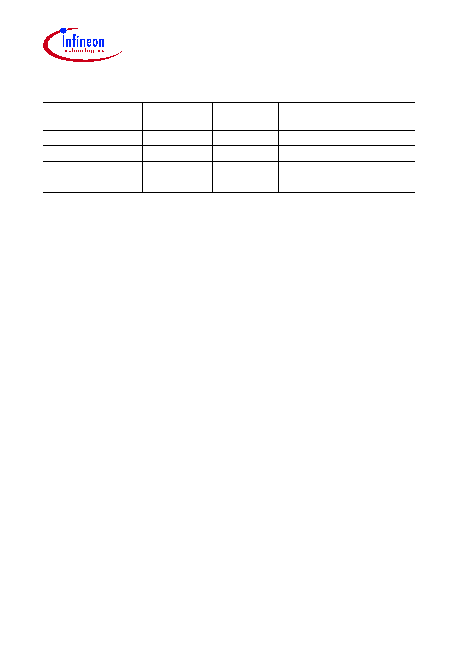
C504
Data Sheet
50
2000-05
Further timing conditions:
t
ADC
min = 500 ns
t
IN
= 2/
f
OSC
= 2
t
CLCL
Notes:
1)
V
AIN
may exceed
V
AGND
or
V
AREF
up to the absolute maximum ratings. However, the conversion result in these
cases will be X000
H
or X3FF
H
, respectively.
2) During the sample time, the input capacitance
C
AIN
can be charged/discharged by the external source. The
internal resistance of the analog source must allow the capacitance to reach their final voltage level within
t
S
.
After the end of the sample time
t
S
, changes of the analog input voltage have no effect on the conversion result.
3) This parameter includes the sample time
t
S
, the time for determining the digital result and the time for the
calibration. Values for the conversion clock
t
ADC
depend on programming and can be taken from the table on
the previous page.
4)
T
UE
is tested at
V
AREF
= 5.0 V,
V
AGND
= 0 V,
V
DD
= 4.9 V. It is guaranteed by design characterization for all other
voltages within the defined voltage range.
If an overload condition occurs on maximum 2 not selected analog input pins and the absolute sum of input
overload currents on all analog input pins does not exceed 10 mA, an additional conversion error of 1/2 LSB
is permissible.
5) During the conversion, the ADC's capacitance must be repeatedly charged or discharged. The internal
resistance of the reference source must allow the capacitance to reach their final voltage level within the
indicated time. The maximum internal resistance results from the programmed conversion timing.
6) Not 100% tested, but guaranteed by design characterization.
Clock Calculation Table
Clock Prescaler
Ratio
ADCL1, 0
t
ADC
t
S
t
ADCC
˜
32
1
1
32
◊
t
IN
64
◊
t
IN
384
◊
t
IN
˜
16
1
0
16
◊
t
IN
32
◊
t
IN
192
◊
t
IN
˜
8
0
1
8
◊
t
IN
16
◊
t
IN
96
◊
t
IN
˜
4
0
0
4
◊
t
IN
8
◊
t
IN
48
◊
t
IN

C504
Data Sheet
51
2000-05
Notes:
1) Interfacing the C504 to devices with float times up to 75 ns is permissible. This limited bus contention will not
cause any damage to Port 0 drivers.
AC Characteristics for C504-L / C504-2R / C504-2E
(Operating Conditions apply)
(
C
L
for Port 0, ALE and PSEN outputs = 100 pF;
C
L
for all other outputs = 80 pF)
Parameter
Symbol
Limit Values
Unit
12-MHz
clock
Variable Clock
1/
t
CLCL
= 3.5 MHz to
12 MHz
min. max. min.
max.
Program Memory Characteristics
ALE pulse width
t
LHLL
CC
127
≠
2
t
CLCL
≠ 40
≠
ns
Address setup to ALE
t
AVLL
CC
43
≠
t
CLCL
≠ 40
≠
ns
Address hold after ALE
t
LLAX
CC
30
≠
t
CLCL
≠ 23
≠
ns
ALE low to valid instr in
t
LLIV
SR
≠
233
≠
4
t
CLCL
≠ 100 ns
ALE to PSEN
t
LLPL
CC
58
≠
t
CLCL
≠ 25
≠
ns
PSEN pulse width
t
PLPH
CC
215
≠
3
t
CLCL
≠ 35
≠
ns
PSEN to valid instr in
t
PLIV
SR
≠
150
≠
3
t
CLCL
≠ 100 ns
Input instruction hold after
PSEN
t
PXIX
SR
0
≠
0
≠
ns
Input instruction float after
PSEN
t
PXIZ
1)
SR
≠
63
≠
t
CLCL
≠ 20
ns
Address valid after PSEN
t
PXAV
1)
CC
75
≠
t
CLCL
≠ 8
≠
ns
Address to valid instr in
t
AVIV
SR
≠
302
≠
5
t
CLCL
≠ 115 ns
Address float to PSEN
t
AZPL
CC
0
≠
0
≠
ns
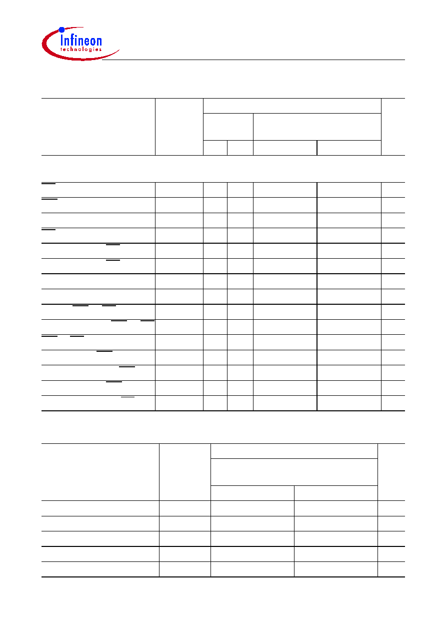
C504
Data Sheet
52
2000-05
AC Characteristics for C504-L / C504-2R / C504-2E (cont'd)
Parameter
Symbol
Limit Values
Unit
12-MHz
clock
Variable Clock
1/
t
CLCL
= 3.5 MHz to 12 MHz
min. max. min.
max.
External Data Memory Characteristics
RD pulse width
t
RLRH
CC 400 ≠
6
t
CLCL
≠ 100
≠
ns
WR pulse width
t
WLWH
CC 400 ≠
6
t
CLCL
≠ 100
≠
ns
Address hold after ALE
t
LLAX2
CC 114 ≠
2
t
CLCL
≠ 53
≠
ns
RD to valid data in
t
RLDV
SR ≠
252
≠
5
t
CLCL
≠ 165
ns
Data hold after RD
t
RHDX
SR 0
≠
0
≠
ns
Data float after RD
t
RHDZ
SR ≠
97
≠
2
t
CLCL
≠ 70
ns
ALE to valid data in
t
LLDV
SR ≠
517
≠
8
t
CLCL
≠ 150
ns
Address to valid data in
t
AVDV
SR ≠
585
≠
9
t
CLCL
≠ 165
ns
ALE to WR or RD
t
LLWL
CC 200 300
3
t
CLCL
≠ 50
3
t
CLCL
+ 50
ns
Address valid to WR or RD
t
AVWL
CC 203 ≠
4
t
CLCL
≠ 130
≠
ns
WR or RD high to ALE high
t
WHLH
CC 43
123
t
CLCL
≠ 40
t
CLCL
+ 40
ns
Data valid to WR transition
t
QVWX
CC 33
≠
t
CLCL
≠ 50
≠
ns
Data setup before WR
t
QVWH
CC 433 ≠
7
t
CLCL
≠ 150
≠
ns
Data hold after WR
t
WHQX
CC 33
≠
t
CLCL
≠ 50
≠
ns
Address float after RD
t
RLAZ
CC ≠
0
≠
0
ns
External Clock Drive Characteristics
Parameter
Symbol
Limit Values
Unit
Variable Clock
Freq. = 3.5 MHz to 12 MHz
min.
max.
Oscillator period
t
CLCL
SR
83.3
294
ns
High time
t
CHCX
SR
20
t
CLCL
≠
t
CLCX
ns
Low time
t
CLCX
SR
20
t
CLCL
≠
t
CHCX
ns
Rise time
t
CLCH
SR
≠
20
ns
Fall time
t
CHCL
SR
≠
20
ns

C504
Data Sheet
53
2000-05
Notes:
1) Interfacing the C504 to devices with float times up to 37 ns is permissible. This limited bus contention will not
cause any damage to Port 0 drivers.
AC Characteristics for C504-L24 / C504-2R24 / C504-2E24
(Operating Conditions apply)
(
C
L
for Port 0, ALE and PSEN outputs = 100 pF;
C
L
for all other outputs = 80 pF)
Parameter
Symbol
Limit Values
Unit
24-MHz
clock
Variable Clock
1/
t
CLCL
= 3.5 MHz to
24 MHz
min.
max.
min.
max.
Program Memory Characteristics
ALE pulse width
t
LHLL
CC 43
≠
2
t
CLCL
≠ 40
≠
ns
Address setup to ALE
t
AVLL
CC 17
≠
t
CLCL
≠ 25
≠
ns
Address hold after ALE
t
LLAX
CC 17
≠
t
CLCL
≠ 25
≠
ns
ALE low to valid instr in
t
LLIV
SR ≠
80
≠
4
t
CLCL
≠ 87 ns
ALE to PSEN
t
LLPL
CC 22
≠
t
CLCL
≠ 20
≠
ns
PSEN pulse width
t
PLPH
CC 95
≠
3
t
CLCL
≠ 30
≠
ns
PSEN to valid instr in
t
PLIV
SR ≠
60
≠
3
t
CLCL
≠ 65 ns
Input instruction hold after
PSEN
t
PXIX
SR 0
≠
0
≠
ns
Input instruction float after
PSEN
t
PXIZ
1)
SR ≠
32
≠
t
CLCL
≠ 10
ns
Address valid after PSEN
t
PXAV
1)
CC 37
≠
t
CLCL
≠ 5
≠
ns
Address to valid instr in
t
AVIV
SR ≠
148
≠
5
t
CLCL
≠ 60 ns
Address float to PSEN
t
AZPL
CC 0
≠
0
≠
ns
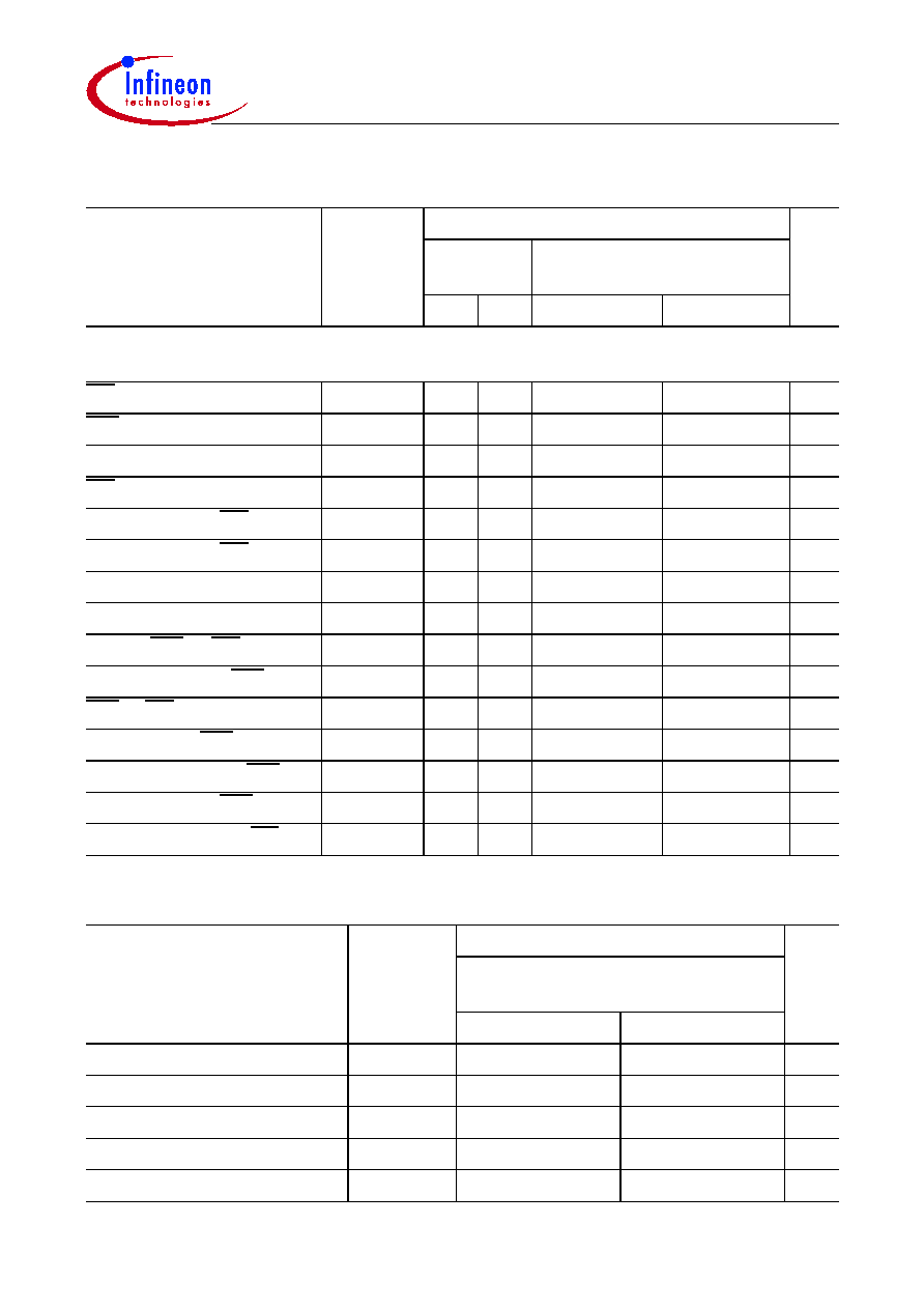
C504
Data Sheet
54
2000-05
AC Characteristics for C504-L24 / C504-2R24 / C504-2E24 (cont'd)
Parameter
Symbol
Limit Values
Unit
24-MHz
clock
Variable Clock
1/
t
CLCL
= 3.5 MHz to 24 MHz
min. max. min.
max.
External Data Memory Characteristics
RD pulse width
t
RLRH
CC 180
≠
6
t
CLCL
≠ 70
≠
ns
WR pulse width
t
WLWH
CC 180
≠
6
t
CLCL
≠ 70
≠
ns
Address hold after ALE
t
LLAX2
CC 56
≠
2
t
CLCL
≠ 27
≠
ns
RD to valid data in
t
RLDV
SR ≠
118
≠
5
t
CLCL
≠ 90
ns
Data hold after RD
t
RHDX
SR 0
≠
0
≠
ns
Data float after RD
t
RHDZ
SR ≠
63
≠
2
t
CLCL
≠ 20
ns
ALE to valid data in
t
LLDV
SR ≠
200
≠
8
t
CLCL
≠ 133
ns
Address to valid data in
t
AVDV
SR ≠
220
≠
9
t
CLCL
≠ 155
ns
ALE to WR or RD
t
LLWL
CC 75
175
3
t
CLCL
≠ 50
3
t
CLCL
+ 50
ns
Address valid to WR
t
AVWL
CC 67
≠
4
t
CLCL
≠ 97
≠
ns
WR or RD high to ALE high
t
WHLH
CC 17
67
t
CLCL
≠ 25
t
CLCL
+ 25
ns
Data valid to WR transition
t
QVWX
CC 5
≠
t
CLCL
≠ 37
≠
ns
Data setup before WR
t
QVWH
CC 170
≠
7
t
CLCL
≠ 122
≠
ns
Data hold after WR
t
WHQX
CC 15
≠
t
CLCL
≠ 27
≠
ns
Address float after RD
t
RLAZ
CC ≠
0
≠
0
ns
External Clock Drive
Parameter
Symbol
Limit Values
Unit
Variable Clock
Freq. = 3.5 MHz to 24 MHz
min.
max.
Oscillator period
t
CLCL
SR 41.7
294
ns
High time
t
CHCX
SR 12
t
CLCL
≠
t
CLCX
ns
Low time
t
CLCX
SR 12
t
CLCL
≠
t
CHCX
ns
Rise time
t
CLCH
SR ≠
12
ns
Fall time
t
CHCL
SR ≠
12
ns
C504
Data Sheet
55
2000-05
Notes:
1) SAK-C504 is not specified for 40 MHz operation.
2) Interfacing the C504 to devices with float times up to 25 ns is permissible. This limited bus contention will not
cause any damage to Port 0 drivers.
Characteristics for C504-L40 / C504-2R40 / C504-2E40
(Operating Conditions apply)
1)
(
C
L
for Port 0, ALE and PSEN outputs = 100 pF;
C
L
for all other outputs = 80 pF)
Parameter
Symbol
Limit Values
Unit
40-MHz
clock
Variable Clock
1/
t
CLCL
= 3.5 MHz to
40 MHz
min.
max.
min.
max.
Program Memory Characteristics
ALE pulse width
t
LHLL
CC 35
≠
2
t
CLCL
≠ 15 ≠
ns
Address setup to ALE
t
AVLL
CC 10
≠
t
CLCL
≠ 15
≠
ns
Address hold after ALE
t
LLAX
CC 10
≠
t
CLCL
≠ 15
≠
ns
ALE low to valid instr in
t
LLIV
SR ≠
55
≠
4
t
CLCL
≠ 45 ns
ALE to PSEN
t
LLPL
CC 10
≠
t
CLCL
≠ 15
≠
ns
PSEN pulse width
t
PLPH
CC 60
≠
3
t
CLCL
≠ 15 ≠
ns
PSEN to valid instr in
t
PLIV
SR ≠
25
≠
3
t
CLCL
≠ 50 ns
Input instruction hold after
PSEN
t
PXIX
SR 0
≠
0
≠
ns
Input instruction float after
PSEN
t
PXIZ
2)
SR ≠
20
≠
t
CLCL
≠ 5
ns
Address valid after PSEN
t
PXAV
2)
CC 20
≠
t
CLCL
≠ 5
≠
ns
Address to valid instr in
t
AVIV
SR ≠
65
≠
5
t
CLCL
≠ 60 ns
Address float to PSEN
t
AZPL
CC ≠ 5
≠
≠ 5
≠
ns
AC
C504
Data Sheet
56
2000-05
AC Characteristics for C504-L40 / C504-2R40 / C504-2E40 (cont'd)
Parameter
Symbol
Limit Values
Unit
40-MHz
clock
Variable Clock
1/
t
CLCL
= 3.5 MHz to 40 MHz
min. max. min.
max.
External Data Memory Characteristics
RD pulse width
t
RLRH
CC 120 ≠
6
t
CLCL
≠ 30
≠
ns
WR pulse width
t
WLWH
CC 120 ≠
6
t
CLCL
≠ 30
≠
ns
Address hold after ALE
t
LLAX2
CC 35
≠
2
t
CLCL
≠ 15
≠
ns
RD to valid data in
t
RLDV
SR ≠
75
≠
5
t
CLCL
≠ 50
ns
Data hold after RD
t
RHDX
SR 0
0
≠
ns
Data float after RD
t
RHDZ
SR ≠
38
≠
2
t
CLCL
≠ 12
ns
ALE to valid data in
t
LLDV
SR ≠
150
≠
8
t
CLCL
≠ 50
ns
Address to valid data in
t
AVDV
SR ≠
150
≠
9
t
CLCL
≠ 75
ns
ALE to WR or RD
t
LLWL
CC 60
90
3
t
CLCL
≠ 15
3
t
CLCL
+ 15
ns
Address valid to WR
t
AVWL
CC 70
≠
4
t
CLCL
≠ 30
≠
ns
WR or RD high to ALE high
t
WHLH
CC 10
40
t
CLCL
≠ 15
t
CLCL
+ 15
ns
Data valid to WR transition
t
QVWX
CC 5
≠
t
CLCL
≠ 20
≠
ns
Data setup before WR
t
QVWH
CC 125 ≠
7
t
CLCL
≠ 50
≠
ns
Data hold after WR
t
WHQX
CC 5
≠
t
CLCL
≠ 20
≠
ns
Address float after RD
t
RLAZ
CC ≠
0
≠
0
ns
External Clock Drive
Parameter
Symbol
Limit Values
Unit
Variable Clock
Freq. = 3.5 MHz to 40 MHz
min.
max.
Oscillator period
t
CLCL
SR 25
294
ns
High time
t
CHCX
SR 10
t
CLCL
≠
t
CLCX
ns
Low time
t
CLCX
SR 10
t
CLCL
≠
t
CHCX
ns
Rise time
t
CLCH
SR ≠
10
ns
Fall time
t
CHCL
SR ≠
10
ns

C504
Data Sheet
57
2000-05
Figure 24
Program Memory Read Cycle
Figure 25
Data Memory Read Cycle
MCT00096
ALE
PSEN
Port 2
LHLL
t
A8 - A15
A8 - A15
A0 - A7
Instr.IN
A0 - A7
Port 0
t
AVLL
PLPH
t
t
LLPL
t
LLIV
t
PLIV
t
AZPL
t
LLAX
t
PXIZ
t
PXIX
t
AVIV
t
PXAV
MCT00097
ALE
PSEN
Port 2
WHLH
t
Port 0
RD
t
LLDV
t
RLRH
t
LLWL
t
RLDV
t
AVLL
t
LLAX2
t
RLAZ
t
AVWL
t
AVDV
t
RHDX
t
RHDZ
A0 - A7 from
Ri or DPL
from PCL
A0 - A7
Instr.
IN
Data IN
A8 - A15 from PCH
P2.0 - P2.7 or A8 - A15 from DPH
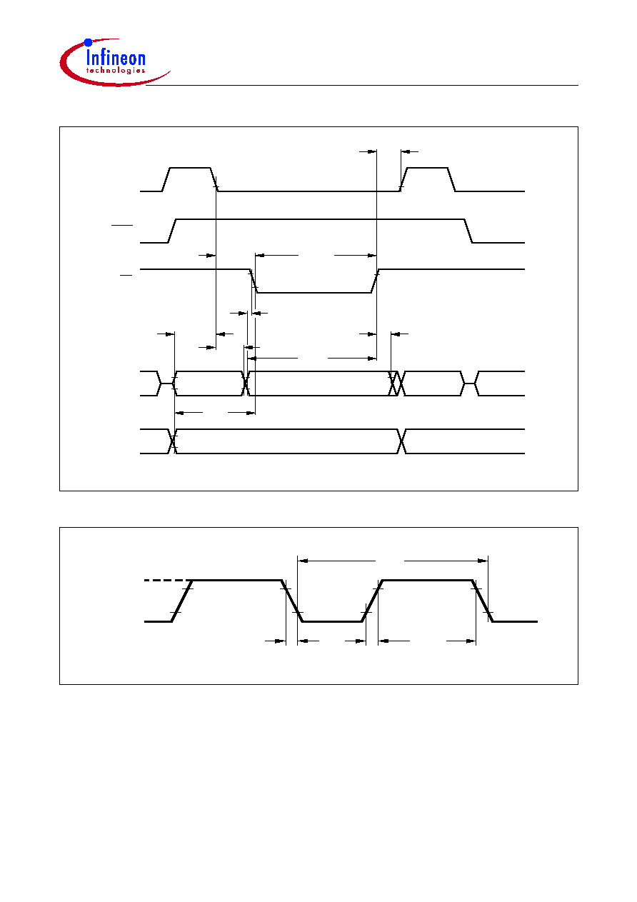
C504
Data Sheet
58
2000-05
Figure 26
Data Memory Write Cycle
Figure 27
External Clock Cycle
MCT00098
ALE
PSEN
Port 2
WHLH
t
Port 0
WR
t
WLWH
t
LLWL
t
QVWX
t
AVLL
t
LLAX2
t
QVWH
t
AVWL
t
WHQX
A0 - A7 from
Ri or DPL
from PCL
A0 - A7
Instr.IN
Data OUT
A8 - A15 from PCH
P2.0 - P2.7 or A8 - A15 from DPH
MCT00033
t
CHCX
t
CLCX
CHCL
t
CLCH
t
V
DD
t
CLCL
- 0.5V
0.45V
DD
0.7
V
V
- 0.1
DD
0.2
C504
Data Sheet
59
2000-05
Note:
V
PP
= 11.5 V
±
5% is valid for devices with version byte 2 = 02
H
or higher. Devices with version byte 2 = 01
H
must
be programmed with
V
PP
= 12 V
±
5%.
AC Characteristics of Programming Mode
(
V
DD
= 5 V
±
10%;
V
PP
= 11.5 V
±
5 %;
T
A
= 25
∞
C
±
10
∞
C)
Parameter
Symbol
Limit Values
Unit
min.
max.
PALE pulse width
t
PAW
35
≠
ns
PMSEL setup to PALE rising edge
t
PMS
10
≠
ns
Address setup to PALE, PROG, or PRD
falling edge
t
PAS
10
≠
ns
Address hold after PALE, PROG, or PRD
falling edge
t
PAH
10
≠
ns
Address, data setup to PROG or PRD
t
PCS
100
≠
ns
Address, data hold after PROG or PRD
t
PCH
0
≠
ns
PMSEL setup to PROG or PRD
t
PMS
10
≠
ns
PMSEL hold after PROG or PRD
t
PMH
10
≠
ns
PROG pulse width
t
PWW
100
≠
µ
s
PRD pulse width
t
PRW
100
≠
ns
Address to valid data out
t
PAD
≠
75
ns
PRD to valid data out
t
PRD
≠
20
ns
Data hold after PRD
t
PDH
0
≠
ns
Data float after PRD
t
PDF
≠
20
ns
PROG high between two consecutive
PROG low pulses
t
PWH1
1
≠
µ
s
PRD high between two consecutive PRD
low pulses
t
PWH2
100
≠
ns
XTAL clock period
t
CLKP
83.3
285.7
ns

C504
Data Sheet
60
2000-05
Figure 28
Programming Code Byte - Write Cycle Timing
t
PAW
t
PMS
PAH
t
PAS
t
A8-A13
A0-A7
D0-D7
PCS
t
PWW
t
PCH
t
t
PWH
MCT03369
H, H
PALE
PMSEL1,0
Port 2
Port 0
PROG
Note: PRD must be high during a programming read cycle

C504
Data Sheet
61
2000-05
Figure 29
Verify Code Byte - Read Cycle Timing
t
PAW
t
PMS
PAH
t
PAS
t
A8-A13
A0-A7
PAD
t
D0-D7
t
PDH
t
PDF
PRD
t
PCS
t
PRW
t
PCH
t
t
PWH
MCT03370
H, H
PALE
PMSEL1,0
Port 2
Port 0
PRD
Note: PROG must be high during a programming read cycle
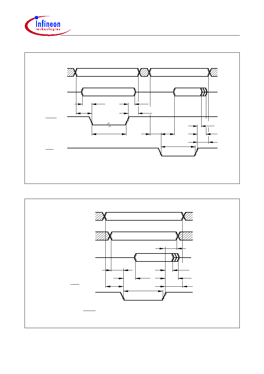
C504
Data Sheet
62
2000-05
Figure 30
Lock Bit Access Timing
Figure 31
Version Byte Read Timing
H, L
H, L
D0, D1
D0, D1
t
PCS
PMS
t
PMH
t
t
PCH
PWW
t
PMS
t
PRD
t
t
PDH
PDF
t
PMH
t
PRW
t
PMSEL1,0
Port 0
PROG
PRD
Note : PALE should be low during a lock bit read / write cycle
MCT03371
e. g. FD
D0-7
t
PCS
PMS
t
t
PDH
PDF
t
PMH
t
MCT03372
Port 2
Port 0
PRD
PMSEL1,0
L, H
H
PRW
t
PRD
t
PCH
t
Note : PROG must be high during a programming read cycle

C504
Data Sheet
63
2000-05
Figure 32
ROM Verification Mode 1
ROM/OTP Verification Characteristics for C504-2R / C504-2E
ROM Verification Mode 1 (C504-2R only)
Parameter
Symbol
Limit Values
Unit
min.
max.
Address to valid data
t
AVQV
≠
10
t
CLCL
ns
P1.0 - P1.7
P2.0 - P2.5
Port 0
Address
Data OUT
Address: P1.0 - P1.7 = A0 - A7
P2.0 - P2.5 = A8 - A13
Data:
P0.0 - P0.7 = D0 - D7
Inputs: P2.6, P2.7, PSEN =
ALE, EA =
RESET =
V
SS
V
IH
V
IH2
AVQV
t
MCT03428

C504
Data Sheet
64
2000-05
Figure 33
ROM Verification Mode 2
ROM/OTP Verification Mode 2
Parameter
Symbol
Limit Values
Unit
min.
typ
max.
ALE pulse width
t
AWD
≠
2
t
CLCL
≠
ns
ALE period
t
ACY
≠
12
t
CLCL
≠
ns
Data valid after ALE
t
DVA
≠
≠
4
t
CLCL
ns
Data stable after ALE
t
DSA
8
t
CLCL
≠
≠
ns
P3.5 setup to ALE low
t
AS
≠
t
CLCL
≠
ns
Oscillator frequency
1/
t
CLCL
4
≠
6
MHz
MCT02613
t
ACY
t
AWD
t
DSA
DVA
t
t
AS
Data Valid
ALE
Port 0
P3.5

C504
Data Sheet
65
2000-05
Figure 34
AC Testing: Input, Output Waveforms
Figure 35
AC Testing: Float Waveforms
Figure 36
Recommended Oscillator Circuits for Crystal Oscillator
AC Inputs during testing are driven at
V
DD
≠ 0.5 V for a logic `1' and 0.45 V for a logic `0'.
Timing measurements are made at
V
IHmin
for a logic `1' and
V
ILmax
for a logic `0'.
0.45 V
V
DD
0.2
-0.1
+0.9
0.2
DD
V
Test Points
MCT00039
V
DD
-0.5 V
For timing purposes a port pin is no longer floating when a 100 mV change from load voltage
occurs and begins to float when a 100 mV change from the loaded
V
OH
/
V
OL
level occurs.
I
OL
/
I
OH
±
20 mA
MCT00038
V
Load
V
Load
-0.1 V
+0.1 V
Load
V
Timing Reference
Points
V
OH
-0.1 V
+0.1 V
OL
V

C504
Data Sheet
66
2000-05
Package Information
GP
M
0
562
2
P-MQFP-44 (SMD)
(Plastic Metric Quad Flat Package)
Sorts of Packing
Package outlines for tubes, trays etc. are contained in our
Data Book "Package Information".
Dimensions in mm
SMD = Surface Mounted Device

Infineon goes for Business Excellence
"Business excellence means intelligent approaches and clearly
defined processes, which are both constantly under review and
ultimately lead to good operating results.
Better operating results and business excellence mean less
idleness and wastefulness for all of us, more professional
success, more accurate information, a better overview and,
thereby, less frustration and more satisfaction."
Dr. Ulrich Schumacher
h t t p : / / w w w . i n f i n e o n . c o m
Published by Infineon Technologies AG