2003-06-27
Page 1
SPP08N50C3, SPI08N50C3
SPA08N50C3
Final data
Cool MOSTM
Power Transistor
V
DS
@
T
jmax
560
V
R
DS(on)
0.6
I
D
7.6
A
Feature
∑
New revolutionary high voltage technology
∑
Ultra low gate charge
∑
Periodic avalanche rated
∑
Extreme dv/dt rated
∑
Ultra low effective capacitances
∑
Improved transconductance
∑
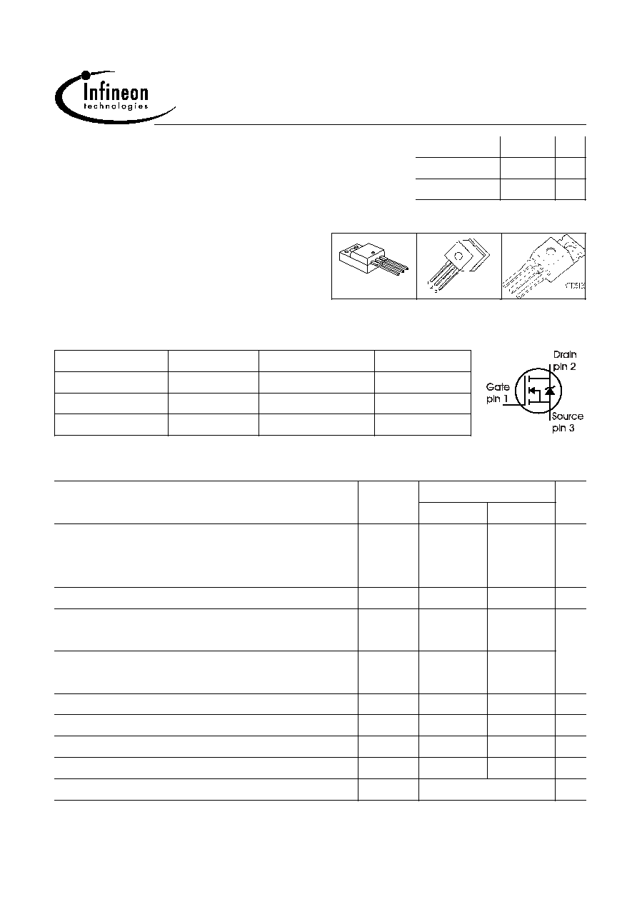
P-TO-220-3-31: Fully isolated package (2500 VAC; 1 minute)
P-TO220-3-31
P-TO262-3-1
P-TO220-3-1
P-TO220-3-31
1
2
3
Marking
08N50C3
08N50C3
08N50C3
Type
Package
Ordering Code
SPP08N50C3
P-TO220-3-1
Q67040-S4567
SPI08N50C3
P-TO262-3-1
Q67040-S4568
SPA08N50C3
P-TO220-3-31 Q67040-S4576
Maximum Ratings
Parameter
Symbol
Value
Unit
SPA
Continuous drain current
T
C
= 25 ∞C
T
C
= 100 ∞C
I
D
7.6
4.6
7.6
1)
4.6
1)
A
Pulsed drain current,
t
p
limited by
T
jmax
I
D puls
22.8
22.8
A
Avalanche energy, single pulse
I
D
=5.5A,
V
DD
=50V
E
AS
230
230
mJ
Avalanche energy, repetitive t
AR
limited by
T
jmax
2)
I
D
=7.6A,
V
DD
=50V
E
AR
0.5
0.5
Avalanche current, repetitive t
AR
limited by
T
jmax
I
AR
7.6
7.6
A
Gate source voltage
V
GS
±20
±20
V
Gate source voltage AC (f >1Hz)
V
GS
±
30
±
30
Power dissipation,
T
C
= 25∞C
P
tot
83
32
W
SPP_I
Operating and storage temperature
T
j ,
T
stg
-55...+150
∞C

2003-06-27
Page 2
SPP08N50C3, SPI08N50C3
SPA08N50C3
Final data
Maximum Ratings
Parameter
Symbol
Value
Unit
Drain Source voltage slope
V
DS
= 400 V, I
D
= 7.6 A,
T
j
= 125 ∞C
dv/dt
50
V/ns
Thermal Characteristics
Parameter
Symbol
Values
Unit
min.
typ.
max.
Thermal resistance, junction - case
R
thJC
-
-
1.5
K/W
Thermal resistance, junction - case, FullPAK
R
thJC_FP
-
-
3.9
Thermal resistance, junction - ambient, leaded
R
thJA
-
-
62
Thermal resistance, junction - ambient, FullPAK
R
thJA FP
-
-
80
Soldering temperature,
1.6 mm (0.063 in.) from case for 10s
3)
T
sold
-
-
260
∞C
Electrical Characteristics, at Tj=25∞C unless otherwise specified
Parameter
Symbol
Conditions
Values
Unit
min.
typ.
max.
Drain-source breakdown voltage
V
(BR)DSS V
GS
=0V, I
D
=0.25mA
500
-
-
V
Drain-Source avalanche
breakdown voltage
V
(BR)DS
V
GS
=0V, I
D
=7.6A
-
600
-
Gate threshold voltage
V
GS(th)
I
D
=350
µ
A, VGS=VDS
2.1
3
3.9
Zero gate voltage drain current
I
DSS
V
DS
=500V,
V
GS
=0V,
T
j
=25∞C
T
j
=150∞C
-
-
0.5
-
1
100
µA
Gate-source leakage current
I
GSS
V
GS
=20V,
V
DS
=0V
-
-
100
nA
Drain-source on-state resistance R
DS(on)
V
GS
=10V, I
D
=4.6A
T
j
=25∞C
T
j
=150∞C
-
-
0.5
1.5
0.6
-
Gate input resistance
R
G
f=1MHz, open drain
-
1.2
-

2003-06-27
Page 3
SPP08N50C3, SPI08N50C3
SPA08N50C3
Final data
Electrical Characteristics
Parameter
Symbol
Conditions
Values
Unit
min.
typ.
max.
Transconductance
g
fs
V
DS
2*I
D
*R
DS(on)max
,
I
D
=4.6A
-
6
-
S
Input capacitance
C
iss
V
GS
=0V,
V
DS
=25V,
f
=1MHz
-
750
-
pF
Output capacitance
C
oss
-
350
-
Reverse transfer capacitance
C
rss
-
12
-
Effective output capacitance,
4)
energy related
C
o(er)
V
GS
=0V,
V
DS
=400
-
56
-
Effective output capacitance,
5)
time related
C
o(tr)
-
30
-
Turn-on delay time
t
d(on)
V
DD
=380V,
V
GS
=0/10V,
I
D
=7.6A,
R
G
=12
-
6
-
ns
Rise time
t
r
-
5
-
Turn-off delay time
t
d(off)
-
60
-
Fall time
t
f
-
7
-
Gate Charge Characteristics
Gate to source charge
Q
gs
V
DD
=400V, I
D
=7.6A
-
3
-
nC
Gate to drain charge
Q
gd
-
17
-
Gate charge total
Q
g
V
DD
=400V, I
D
=7.6A,
V
GS
=0 to 10V
-
32
-
Gate plateau voltage
V
(plateau)
V
DD
=400V, I
D
=7.6A
-
5
-
V
1Limited only by maximum temperature
2Repetitve avalanche causes additional power losses that can be calculated as P
AV
=
E
AR
*
f
.
3Soldering temperature for TO-263: 220∞C, reflow
4C
o(er)
is a fixed capacitance that gives the same stored energy as
C
oss
while
V
DS
is rising from 0 to 80% V
DSS
.
5C
o(tr)
is a fixed capacitance that gives the same charging time as
C
oss
while
V
DS
is rising from 0 to 80% V
DSS
.
2003-06-27
Page 4
SPP08N50C3, SPI08N50C3
SPA08N50C3
Final data
Electrical Characteristics
Parameter
Symbol
Conditions
Values
Unit
min.
typ.
max.
Inverse diode continuous
forward current
I
S
T
C
=25∞C
-
-
7.6
A
Inverse diode direct current,
pulsed
I
SM
-
-
22.8
Inverse diode forward voltage
V
SD
V
GS
=0V, I
F
=I
S
-
1
1.2
V
Reverse recovery time
t
rr
V
R
=400V, I
F
=I
S
,
di
F
/dt
=100A/µs
-
370
-
ns
Reverse recovery charge
Q
rr
-
3.6
-
µC
Peak reverse recovery current
I
rrm
-
25
-
A
Peak rate of fall of reverse
recovery current
di
rr
/dt
T
j
=25∞C
-
700
-
A/µs
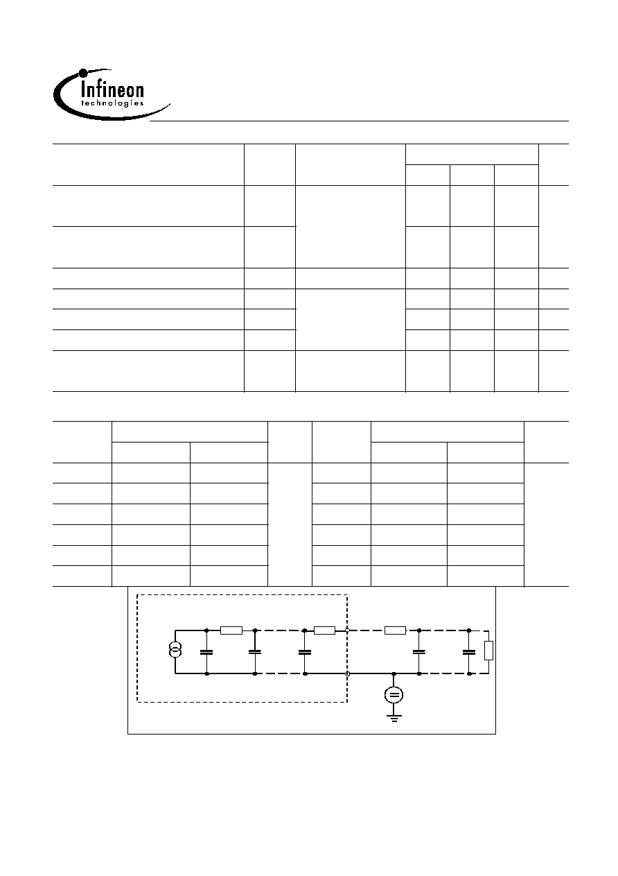
Typical Transient Thermal Characteristics
Symbol
Value
Unit
Symbol
Value
Unit
SPA
SPA
R
th1
0.024
0.024
K/W
C
th1
0.00012
0.00012
Ws/K
R
th2
0.046
0.046
C
th2
0.0004578
0.0004578
R
th3
0.085
0.085
C
th3
0.000645
0.000645
R
th4
0.308
0.195
C
th4
0.001867
0.001867
R
th5
0.317
0.45
C
th5
0.004795
0.007558
R
th6
0.112
2.511
C
th6
0.045
0.412
SPP_B
SPP_B
External Heatsink
T
j
T
case
T
am b
C
th1
C
th2
R
th1
R
th,n
C
th,n
P
tot
(t)
2003-06-27
Page 5
SPP08N50C3, SPI08N50C3
SPA08N50C3
Final data
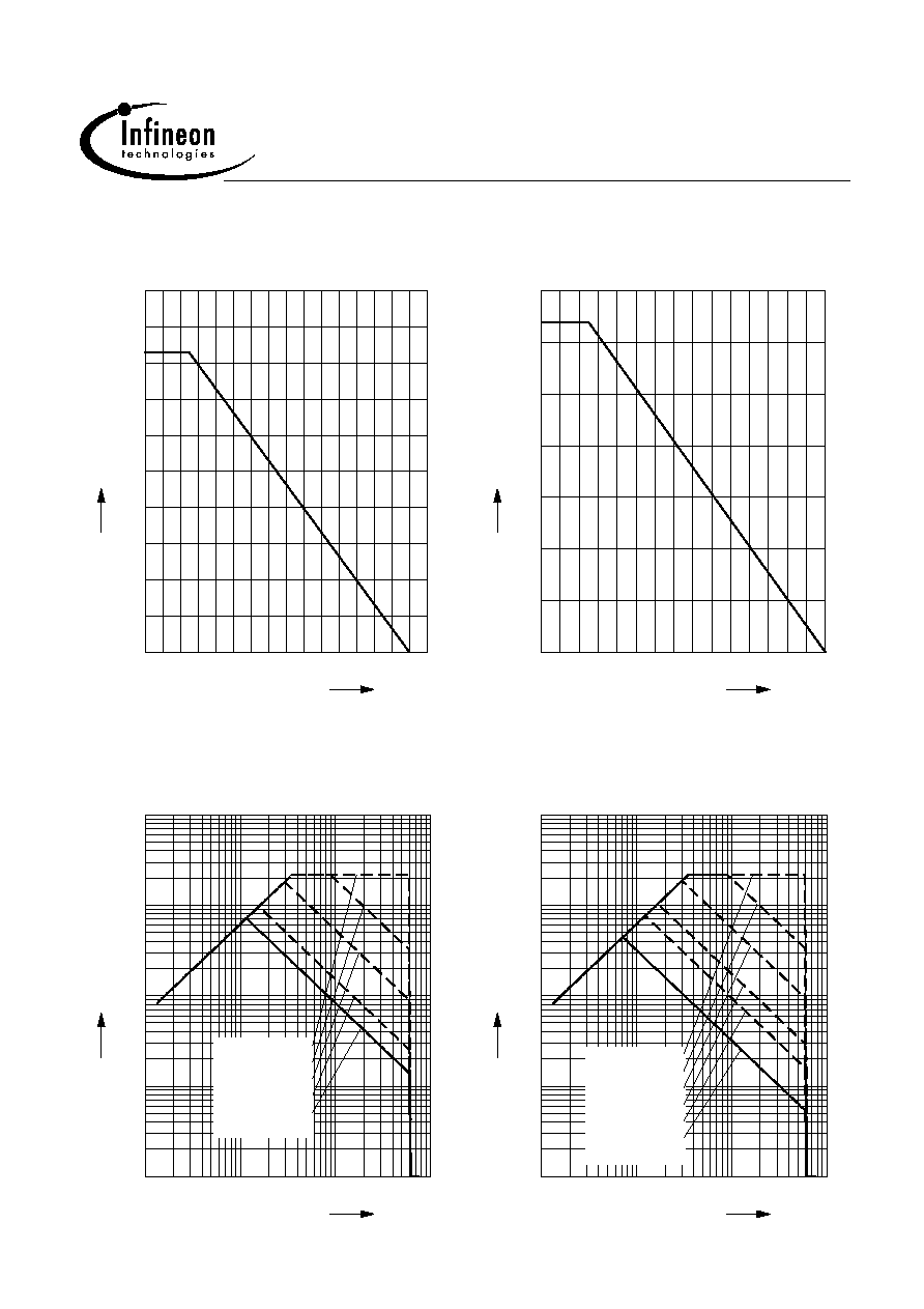
1 Power dissipation
P
tot
= f (
T
C
)
0
20
40
60
80
100
120
∞C
160
T
C
0
10
20
30
40
50
60
70
80
W
100
SPP08N50C3
P
tot
2 Power dissipation FullPAK
P
tot
= f (
T
C
)
0
20
40
60
80
100
120
∞C
150
T
C
0
5
10
15
20
25
W
35
P
tot
3 Safe operating area
I
D
= f ( V
DS
)
parameter : D = 0 ,
T
C
=25∞C
10
0
10
1
10
2
10
3
V
V
DS
-2
10
-1
10
0
10
1
10
2
10
A
I
D
tp = 0.001 ms
tp = 0.01 ms
tp = 0.1 ms
tp = 1 ms
DC
4 Safe operating area FullPAK
I
D
= f (
V
DS
)
parameter: D = 0,
T
C
= 25∞C
10
0
10
1
10
2
10
3
V
V
DS
-2
10
-1
10
0
10
1
10
2
10
A
I
D
tp = 0.001 ms
tp = 0.01 ms
tp = 0.1 ms
tp = 1 ms
tp = 10 ms
DC