 | –≠–ª–µ–∫—Ç—Ä–æ–Ω–Ω—ã–π –∫–æ–º–ø–æ–Ω–µ–Ω—Ç: TDA6170 | –°–∫–∞—á–∞—Ç—å:  PDF PDF  ZIP ZIP |

Data Sheet
07.99
TDA6170X
Satellite Sound IF
with Wegener Expander
Components
for Entertainment Electronics

Edition 07.99
Published by Siemens AG,
Bereich Halbleiter, Marketing-
Kommunikation, Balanstraþe 73,
81541 M¸nchen
©
Siemens AG 1995.
All Rights Reserved.
Attention please!
As far as patents or other rights of third parties
are concerned, liability is only assumed for
components, not for applications, processes
and circuits implemented within components
or assemblies.
The information describes the type of compo-
nent and shall not be considered as assured
characteristics.
Terms of delivery and rights to change design
reserved.
For questions on technology, delivery and
prices please contact the Semiconductor
Group Offices in Germany or the Siemens
Companies and Representatives worldwide
(see address list).
Due to technical requirements components
may contain dangerous substances. For infor-
mation on the types in question please contact
your nearest Siemens Office, Semiconductor
Group.
Siemens AG is an approved CECC manufac-
turer.
Packing
Please use the recycling operators known to
you. We can also help you ≠ get in touch with
your nearest sales office. By agreement we
will take packing material back, if it is sorted.
You must bear the costs of transport.
For packing material that is returned to us
unsorted or which we are not obliged to
accept, we shall have to invoice you for any
costs incurred.
Components used in life-support devices
or systems must be expressly authorized
for such purpose!
Critical components
1
of the Semiconductor
Group of Siemens AG, may only be used in
life-support devices or systems
2
with the
express written approval of the Semiconductor
Group of Siemens AG.
1 A critical component is a component used
in a life-support device or system whose
failure can reasonably be expected to
cause the failure of that life-support device
or system, or to affect its safety or effec-
tiveness of that device or system.
2 Life support devices or systems are
intended (a) to be implanted in the human
body, or (b) to support and/or maintain and
sustain human life. If they fail, it is reasona-
ble to assume that the health of the user
may be endangered.
Ausgabe 07.99
Herausgegeben von Siemens AG,
Bereich Halbleiter, Marketing-
Kommunikation, Balanstraþe 73,
81541 M¸nchen
©
Siemens AG 1995.
Alle Rechte vorbehalten.
Wichtige Hinweise!
Gew‰hr f¸r die Freiheit von Rechten Dritter
leisten wir nur f¸r Bauelemente selbst, nicht
f¸r Anwendungen, Verfahren und f¸r die in
Bauelementen oder Baugruppen realisierten
Schaltungen.
Mit den Angaben werden die Bauelemente
spezifiziert, nicht Eigenschaften zugesichert.
Liefermˆglichkeiten und technische ƒnderun-
gen vorbehalten.
Fragen ¸ber Technik, Preise und Liefermˆgli-
chkeiten richten Sie bitte an den Ihnen n‰chst-
gelegenen Vertrieb Halbleiter in Deutschland
oder an unsere Landesgesellschaften im Aus-
land.
Bauelemente kˆnnen aufgrund technischer
Erfordernisse Gefahrstoffe enthalten.
Ausk¸nfte dar¸ber bitten wir unter Angabe
des betreffenden Typs ebenfalls ¸ber den Ver-
trieb Halbleiter einzuholen.
Die Siemens AG ist ein Hersteller von CECC-
qualifizierten Produkten.
Verpackung
Bitte benutzen Sie die Ihnen bekannten Verw-
erter. Wir helfen Ihnen auch weiter ≠ wenden
Sie sich an Ihren f¸r Sie zust‰ndigen Vertrieb
Halbleiter. Nach R¸cksprache nehmen wir
Verpackungsmaterial sortiert zur¸ck. Die
Transportkosten m¸ssen Sie tragen.
F¸r Verpackungsmaterial, das unsortiert an
uns zur¸ckgeliefert wird oder f¸r das wir keine
R¸cknahmepflicht haben, m¸ssen wir Ihnen
die anfallenden Kosten in Rechnung stellen.
Bausteine in lebenserhaltenden Ger‰ten
oder Systemen m¸ssen ausdr¸cklich daf¸r
zugelassen sein!
Kritische Bauelemente
1
des Bereichs Hal-
bleiter der Siemens AG d¸rfen nur mit aus-
dr¸cklicher schriftlicher Genehmigung des
Bereichs Halbleiter der Siemens AG in leb-
enserhaltenden Ger‰ten oder Systemen
2
eingesetzt werden.
1 Ein kritisches Bauelement ist ein in einem
lebenserhaltenden Ger‰t oder System
eingesetztes Bauelement, bei dessen Aus-
fall berechtigter Grund zur Annahme
besteht, daþ das lebenserhaltende Ger‰t
oder System ausf‰llt bzw. dessen Sicher-
heit oder Wirksamkeit beeintr‰chtigt wird.
2 Lebenserhaltende Ger‰te und Systeme
sind (a) zur chirurgischen Einpflanzung in
den menschlichen Kˆrper gedacht, oder
(b) unterst¸tzen bzw. erhalten das men-
schliche Leben. Sollten sie ausfallen,
besteht berechtigter Grund zur Annahme,
daþ die Gesundheit des Anwenders
gef‰hrdet werden kann.

TDA6170X
Revision History:Current Version: 07.99
Previous Version:
old Page
new Page
Subjects (major changes since last revision)
Data Classification
Maximum Ratings
Maximum ratings are absolute ratings; exceeding only one of these values may cause irreversible damage to
the integrated circuit.
Characteristics
The listed characteristics are ensured over the operating range of the integrated circuit. Typical characteristics
specify mean values expected over the production spread. If not otherwise specified, typical characteristics
apply at
T
A
= 25
∞
C and the given supply voltage.
Operating Range
In the operating range the functions given in the circuit description are fulfilled.
For detailed technical information about "Processing Guidelines" and
"Quality Assurance" for ICs, see our "Product Overview".

Semiconductor Group
21.7.99
Data Sheet
TDA6170X
1
Features
. . . . . . . . . . . . . . . . . . . . . . . . . . . . . . . . . . . . . . . . . . . . . . . . . . . . . . . . . 1
2
Pinning
. . . . . . . . . . . . . . . . . . . . . . . . . . . . . . . . . . . . . . . . . . . . . . . . . . . . . . . . . . 1
3
Ordering Information
. . . . . . . . . . . . . . . . . . . . . . . . . . . . . . . . . . . . . . . . . . . . . . . 1
4
General Description
. . . . . . . . . . . . . . . . . . . . . . . . . . . . . . . . . . . . . . . . . . . . . . . . 1
4.1
Application
. . . . . . . . . . . . . . . . . . . . . . . . . . . . . . . . . . . . . . . . . . . . . . . . . . . . . . . . 1
5
Pinconfiguration
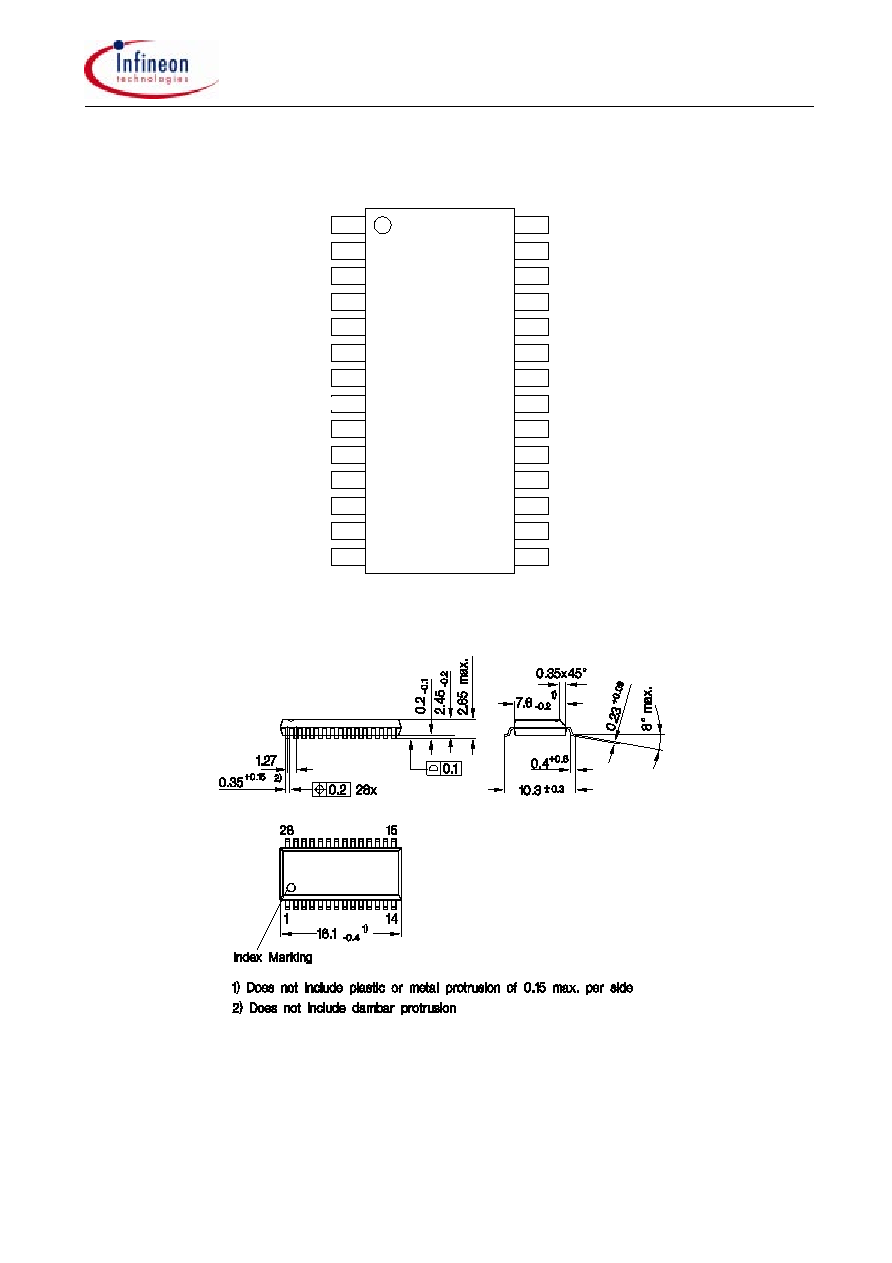
. . . . . . . . . . . . . . . . . . . . . . . . . . . . . . . . . . . . . . . . . . . . . . . . . . 2
5.1
Package outline P-DSO-28-1
. . . . . . . . . . . . . . . . . . . . . . . . . . . . . . . . . . . . . . . . . . 2
6
Pin Definitions and Functions
. . . . . . . . . . . . . . . . . . . . . . . . . . . . . . . . . . . . . . . 3
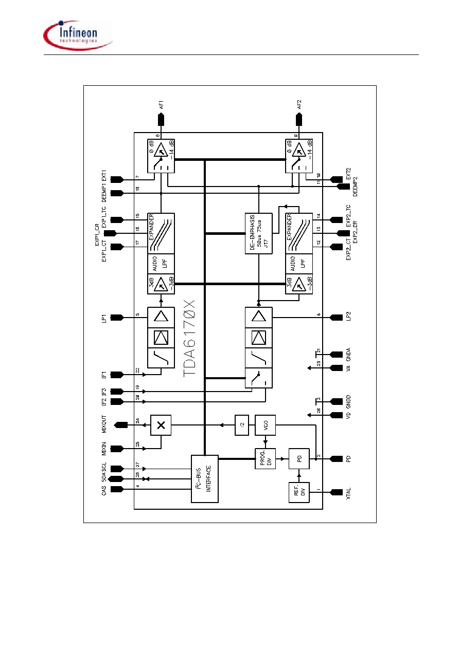
7
Block Diagram
. . . . . . . . . . . . . . . . . . . . . . . . . . . . . . . . . . . . . . . . . . . . . . . . . . . . 4
8
Circuit Description
. . . . . . . . . . . . . . . . . . . . . . . . . . . . . . . . . . . . . . . . . . . . . . . . . 5
8.1
General
. . . . . . . . . . . . . . . . . . . . . . . . . . . . . . . . . . . . . . . . . . . . . . . . . . . . . . . . . . 5
8.2
PLL Description
. . . . . . . . . . . . . . . . . . . . . . . . . . . . . . . . . . . . . . . . . . . . . . . . . . . . 5
8.3
Fast I
2
C-Bus Interface
. . . . . . . . . . . . . . . . . . . . . . . . . . . . . . . . . . . . . . . . . . . . . . . 5
8.3.1
Logic Allocation
. . . . . . . . . . . . . . . . . . . . . . . . . . . . . . . . . . . . . . . . . . . . . . . . . . . . 6
8.3.2
IF-Muting
. . . . . . . . . . . . . . . . . . . . . . . . . . . . . . . . . . . . . . . . . . . . . . . . . . . . . . . . . 6
8.4
Converter Mixer
. . . . . . . . . . . . . . . . . . . . . . . . . . . . . . . . . . . . . . . . . . . . . . . . . . . . 6
8.5
IF Limiter with Demodulator
. . . . . . . . . . . . . . . . . . . . . . . . . . . . . . . . . . . . . . . . . . . 6
8.6
Expander Description
. . . . . . . . . . . . . . . . . . . . . . . . . . . . . . . . . . . . . . . . . . . . . . . 7
8.7
AF Switch and Volume Control
. . . . . . . . . . . . . . . . . . . . . . . . . . . . . . . . . . . . . . . . 7
9
Pinning
. . . . . . . . . . . . . . . . . . . . . . . . . . . . . . . . . . . . . . . . . . . . . . . . . . . . . . . . . . 8
10
Absolute Maximum Ratings
. . . . . . . . . . . . . . . . . . . . . . . . . . . . . . . . . . . . . . . . 15
11
Operating Range
. . . . . . . . . . . . . . . . . . . . . . . . . . . . . . . . . . . . . . . . . . . . . . . . . 16
12
Electrical Characteristics
. . . . . . . . . . . . . . . . . . . . . . . . . . . . . . . . . . . . . . . . . . 17
13
Application Circuit
. . . . . . . . . . . . . . . . . . . . . . . . . . . . . . . . . . . . . . . . . . . . . . . . 21
14
Test circuit
. . . . . . . . . . . . . . . . . . . . . . . . . . . . . . . . . . . . . . . . . . . . . . . . . . . . . . 22
15
Diagrams
. . . . . . . . . . . . . . . . . . . . . . . . . . . . . . . . . . . . . . . . . . . . . . . . . . . . . . . 23
15.1
I
2
C-Bus Timing
. . . . . . . . . . . . . . . . . . . . . . . . . . . . . . . . . . . . . . . . . . . . . . . . . . . 23
Semiconductor Group
1
21.7.99
Satellite Sound IF
TDA6170X
with Wegener Expander
Data Sheet
BIPOLAR
1
Features
∑
Fast I
2
C-bus controlled (max. 400 kHz)
∑
PLL controlled sound IF tuning with
10 kHz stepwidth
∑
Second order high-pass mixer input
∑
IF MUX for 10.7 MHz
broad / small IF filters
∑
Two identical high sensitive alignment free
FM demodulators
∑
Original Wegener PANDA 1
TM
expander
∑
Volume control for individual settings
∑
50
µ
s / 75
µ
s / J17 de-emphasis for main
sound reception
∑
Fully ESD protection
P-DSO-28
Package
2
Ordering Information
3
General Description
Multistandard satellite sound IF device consisting of a mixer and a voltage controlled oscillator (VCO) as a fre-
quency converter that can be continuously tuned in 10 kHz increments with crystal accuracy by means of a
PLL, two FM limiter amplifiers with PLL FM demodulators followed by two Wegener PANDA1
TM
expanders.
The AF signal passes through two switches. Each switch can select the AF sources and the mono / stereo
mode the de-emphasis networks together with the two following volume control stages with audio buffers.
In front of one FM section an IF multiplexer is used to select the IF bandwidth.
The switching functions and settings of the PLL are controlled by an I
2
C-bus.
3.1
Application
∑
For use in satellite receivers
Type
Package
Ordering Code
TDA6170X
P-DSO-28-1
Q67001-A5214
Data Sheet
TDA6170X
Semiconductor Group
2
21.7.99
4
Pinconfiguration
4.1
Package outline P-DSO-28-1
SDA
SCL
VD
IF1
VA
MIXOUT
MIXIN
GNDA
IF2
IF3
EXP1 TC
EXP1 C
R
EXP1 C
T
DEEMP1
XTAL
PD
GNDD
EXT1
LP2
LP1
CAS
AF1
AF2
EXT2
EXP2 TC
EXP2 C
R
EXP2 C
T
DEEMP2
18
17
16
15
20
21
19
24
23
22
25
26
1
11
12
13
14
9
8
10
5
6
7
3
4
2
28
27
P-DSO 28-1

Data Sheet
TDA6170X
Semiconductor Group
3
21.7.99
5
Pin Definitions and Functions
Pin No.
Symbol
Function
1
XTAL
crystal input for 4 MHz oscillator
2
PD
synthesizer loop-filter
3
GNDD
I
2
C-bus and synthesizer ground
4
CAS
I
2
C-bus address selection
5
LP1
FM-PLL lowpass capacitor (channel 1)
6
LP2
FM-PLL lowpass capacitor (channel 2)
7
EXT1
external audio input (channel 1)
8
AF1
audio output (channel 1)
9
AF2
audio output (channel 2)
10
EXT2
external audio input (channel 2)
11
DEEMP2
de-emphasis capacitor (channel 2)
12
EXP2 C
T
expander tracking capacitor (channel 2)
13
EXP2 C
R
expander release capacitor (channel 2)
14
EXP2 TC
expander time constant (channel 2)
15
EXP1 TC
expander time constant (channel 1)
16
EXP1 C
R
expander release capacitor (channel 1)
17
EXP1 C
T
expander tracking capacitor (channel 1)
18
DEEMP1
de-emphasis capacitor (channel 1)
19
IF3
intercarrier input 3
20
IF2
intercarrier input 2
21
GNDA
analog ground
22
IF1
intercarrier input 1
23
VA
analog supply voltage (+8V)
24
MIXOUT
intercarrier mixer output
25
MIXIN
mixer input
26
VD
I
2
C-bus and synthesizer supply voltage (+5V)
27
SCL
I
2
C-bus serial clock input
28
SDA
I
2
C-bus serial data input/output
Data Sheet
TDA6170X
Semiconductor Group
4
21.7.99
6
Block Diagram

Data Sheet
TDA6170X
Semiconductor Group
5
21.7.99
7
Circuit Description
7.1
General
The sound intermediate frequencies contained in the baseband of a demodulated FM satellite signal can lie
between 5 and 9.9 MHz. This band of frequencies is applied rough filtered to the high-pass input of the con-
verter mixer. The purpose of this mixer is to convert the different sound IF`s in the baseband to fixed output
frequencies (e.g. 10.7 / 10.72 MHz). These frequencies are then fed by external filters to the three sound IF
inputs.
The VCO of the mixer can be continuously tuned between 29 and 40 MHz in 20 kHz increments with crystal
accuracy by means of a PLL circuit.
The settings of the programmable divider and switching of the IF MUX and de-emphasis networks and volume
control are done by the I
2
C-bus.
Pin 5 (CAS) offers two switchable chip addresses to enable parallel operation of two devices.
All pins are guarded against electrostatic discharge. SCL and SDA include special protective structures to
permit continued bus operation when the device is switched off.
7.2
PLL Description
The VCO signal is applied to the PLL input. It passes through a programmable divider (N=1024 to 2047) and
then compared with a reference frequency (f
REF
= 20 kHz in a digital frequency / phase detector. This fre-
quency is derived from a 4 MHz crystal oscillator whose signal is divided by 200.
The phase detector has a charge pump push-pull current output. If the negative edge of the divided VCO sig-
nal appears before the negative edge of the reference signal, the current source I+ will pulse for the duration
of the phase difference. In the reverse case it is the current sink I-. If both signals are in phase, the output has
a high impedance and the PLL is locked. The current pulses are filtered by means of an integrator.
The pump current can be switched between two values (1 and 5) by software with a control bit 5I. This permits
a change in the control response during and after lock-in state.
7.3
Fast I
2
C-Bus Interface
Information is exchanged between the processor and the sound IF device on an fast asynchronous bidirec-
tional data bus. The timing for this comes from the processor (input SCL), while pin SDA functions as an I/O
depending on the direction of the data (open collector; external pull-up resistor). The bus will work with clock
frequencies up to 400 kHz.
The data from the processor goes to an I
2
C-bus controller and are put into registers (latches 0 to x) according
to their function. When the bus is not busy, both lines are in the marking state (SDA, SCL are high). Each tel-
egram begins with the start condition: SDA goes low while SCL remains high. All further exchanges of infor-
mation occur when SCL is low and are read by the controller with the positive clock edge. If SDA goes high
while the clock is high, the I
2
C-bus interface recognizes this as a stop condition and thus the end of the tele-
gram.
For what follows, refer to the table of logic assignments below.
All telegrams are transferred byte for byte, followed by a ninth clock pulse during which the controller pulls the
SDA line to low (i.e. acknowledge condition). The first byte consists of seven address bits with which the proc-
essor selects the PLL from among several other peripheral devices (chip select). The eighth bit is always low.
The first bit of the first or third data byte in the data part of the telegram determines whether a divider ratio or
control information for the IF or audio part will follow. In every case the first byte must be followed by a byte of
the same data type (or stop condition). When the supply voltage is applied, a power-on reset circuit prevents
the PLL from pulling the SDA line to low and thus blocking the bus.
Data Sheet
TDA6170X
Semiconductor Group
6
21.7.99
7.3.1
Logic Allocation
7.3.2
IF-Muting
7.4
Converter Mixer
In the converter mixer the sound subcarriers (frequency band approx. 5 to 9.9 MHz) contained in the base-
band of the received composite satellite signal are converted to an output frequency of 10.52 MHz and 10.7
MHz for example. The converter consists of a high-pass input filter followed by a double balanced mixer and a
low impedance output.
The signal of the on chip voltage controlled oscillator (VCO) is applied to the PLL input.
7.5
IF Limiter with Demodulator
The two limiter amplifiers are implemented as balanced five stage, capacitively coupled differential amplifiers.
The three inputs are designed as high-pass inputs. The load resistors for the IF filters are connected to
ground.
The output signals of the limiter amplifiers are fed directly to the internal PLL FM demodulators.
The demodulated AF signals are fed to the input of a pre volume control part in front of the expander the de-
emphasis networks and audio switches.
Byte
Data
Remarks
Address Byte
0
1
0
0
0
0
MA
R/W
A
Progr. Divider Byte 1
0
0
N11
N10
N9
N8
N7
N6
A
Progr. Divider Byte 2
0
0
N5
N4
N3
N2
N1
N0
A
Control Byte 1
1
5I
Z2
Z1
Z0
X
X
X
A
Control Byte 2
1
VL2
VL1
VL0
VR2
VR1
VR0
X
A
Control Byte 3
1
PVL2
PVL1
PVL0 PVR2 PVR1 PVR0
X
A
Address Byte 1
1
1. Chip address (CAS) Pin 5 grounded
0
1
0
0
0
1
0
0
A
=H44
Address Byte 2
2
2. Chip address (CAS) Pin 5 open
0
1
0
0
0
1
1
0
A
=H46
Control Bits
IF-Source
Function
Z2
Z1
Z0
IF1
IF2
IF3
0
0
0
on
on
off
expanders are working, audio = stereo
0
0
1
off
on
off
expanders are working, audio = mono
0
1
0
on
off
off
expanders are working, audio = mono
0
1
1
off
off
on
de-emphasis = 50
µ
; audio = mono
1
0
0
off
off
on
de-emphasis = 75
µ
; audio = mono
1
0
1
off
off
on
de-emphasis = J17; audio = mono
1
1
0
off
off
off
External audio
1
1
1
off
off
off
Mute

Data Sheet
TDA6170X
Semiconductor Group
7
21.7.99
7.6
Expander Description
The demodulated and level controlled audio signals are fed via low-pass filters to the inputs of two identical
expander circuits. The IF3 audio signal is also applied in parallel via different de-emphasis networks to the
input of the audio switch for broadband mono reception. The expander circuits have the reverse characteris-
tics of the audio compressor of the TV station. A 3 bit pre volume control (control byte 3: PVL2...PVL0 and
PVR2...PVR0) for each audio channel enables a correct adjustment of the expander characteristics and
allows the possibility to align to the right level for both broadband and smallband sound IF reception.
7.7
AF Switch and Volume Control
The input signals of the AF switch can be derived from the external audio input pair. However, these signals
can also be derived from either the different de-emphasis networks or from both expanders. The selection of
the output signals from IF1, IF2 or IF3 is done by using the I
2
C-bus interface. The switches are followed by a
volume control section with buffered outputs Ch1 and Ch2.
In case of small-band reception the demodulated signals of IF1 and IF2 are processed in both expanders and
fed to the switches. So it is possible to select one of each or both in the audio switches for both AF outputs
Ch1 and Ch2.
In the case of broad-band audio transmission with 50
µ
s, 75
µ
s or J17 pre-emphasis the IF3 input is active and
with the audio switch the demodulated audio signals are selected after the three de-emphasis networks and
fed to both AF outputs in mono mode.
The 3 bit volume control (control byte 2: VL2...VL0 and VR2...VR0) in front of each AF output enables the
same audio level for different FM deviations of several satellite transponders.
Data Sheet
TDA6170X
Semiconductor Group
8
21.7.99
8
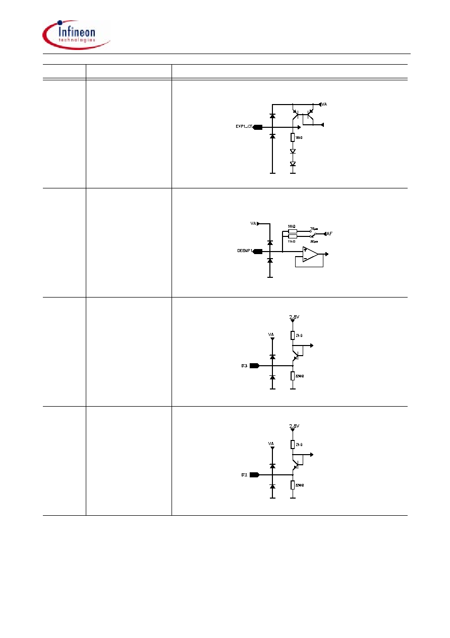
Pinning
Pin No.
Symbol
Equivalent Circuit
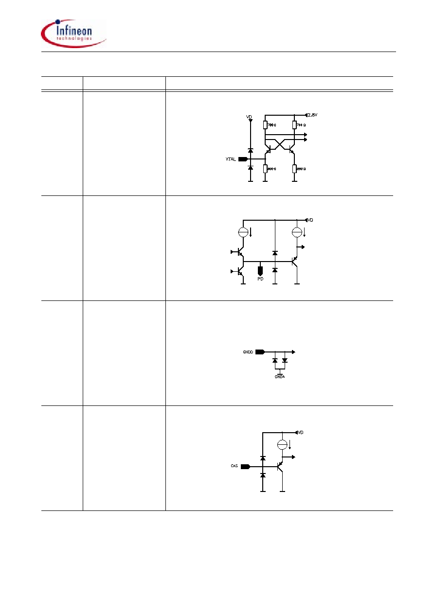
1
XTAL
2
PD
3
GNDD
4
CAS
Data Sheet
TDA6170X
Semiconductor Group
9
21.7.99
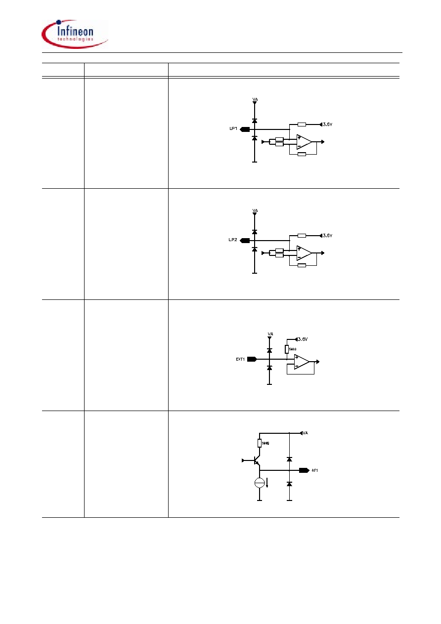
5
LP1
6
LP2
7
EXT1
8
AF1
Pin No.
Symbol
Equivalent Circuit
Data Sheet
TDA6170X
Semiconductor Group
10
21.7.99
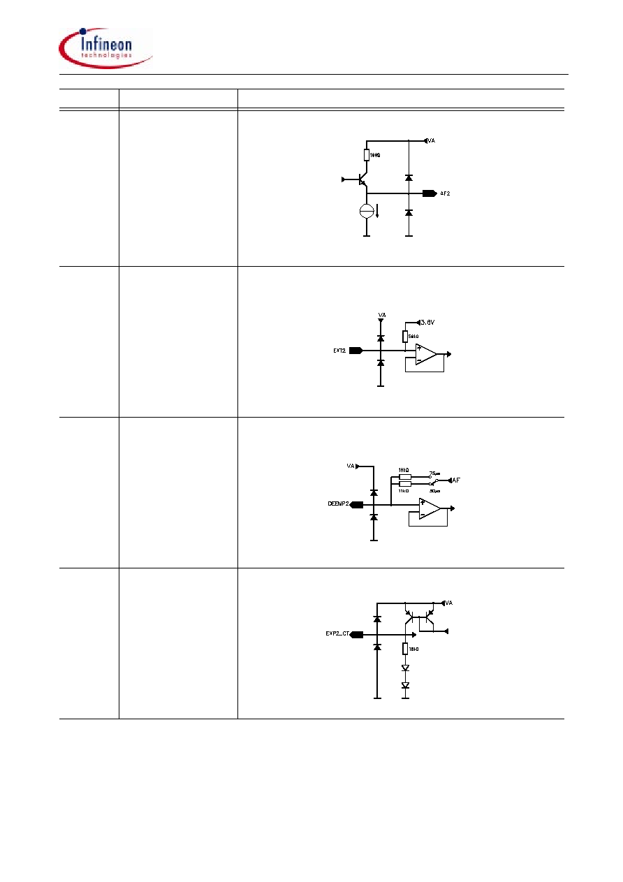
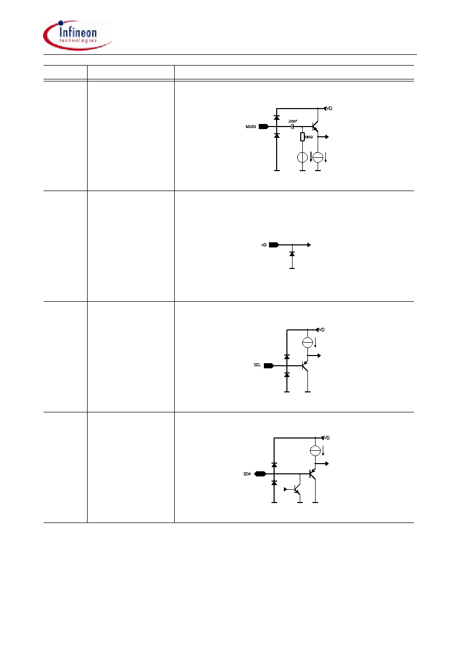
9
AF2
10
EXT2
11
DEEMP2
12
EXP2 C
T
Pin No.
Symbol
Equivalent Circuit
Data Sheet
TDA6170X
Semiconductor Group
11
21.7.99
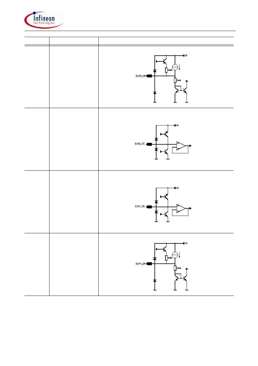
13
EXP2 C
R
14
EXP2 TC
15
EXP1 TC
16
EXP1 C
R
Pin No.
Symbol
Equivalent Circuit
Data Sheet
TDA6170X
Semiconductor Group
12
21.7.99
17
EXP1 C
T
18
DEEMP1
19
IF3
20
IF2
Pin No.
Symbol
Equivalent Circuit

Data Sheet
TDA6170X
Semiconductor Group
13
21.7.99
21
GNDA
22
IF1
23
VA
24
MIXOUT
Pin No.
Symbol
Equivalent Circuit
Data Sheet
TDA6170X
Semiconductor Group
14
21.7.99
25
MIXIN
26
VD
27
SDA
28
SCL
Pin No.
Symbol
Equivalent Circuit

Data Sheet
TDA6170X
Semiconductor Group
15
21.7.99
9
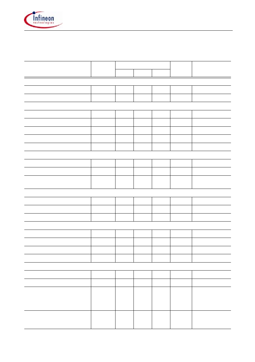
Absolute Maximum Ratings
The maximal ratings may not be exceeded under any circumstances, not even momentary and individual, as
permanent damage to the IC will result.
Ambient Temperature under bias: T
A
=0 to 70
∞
C
All values are referred to ground (pin), unless stated otherwise.
All currents are designated according to the source and sink principle, i.e. if the device pin is to be regarded as a sink (the current
flows into the stated pin to internal ground), it has a negative sign, and if it is a source (the current flows from Vs across the
designated pin), it has a positive sign.
Parameter
Symbol
Limit Values
Unit
Test Conditions
min
max
Supply voltage (digital)
V
VD
0
6
V
Supply voltage (analog)
V
VA
0
13.2
V
Mixer input
V
MIXIN
-0.3
13.2
V
IF inputs
V
IF
-0.3
1
V
Crystal oscillator
V
XTAL
0
1.5
V
SDA; SCL; CAS
V
-0.3
6
V
Junction temperature
T
j
0
150
∞
C
Storage temperature
T
stg
0
125
∞
C
Thermal resistance
R
th j-a
75
K/W
ESD-Protection
V
ESD
2
kV
all pins

Data Sheet
TDA6170X
Semiconductor Group
16
21.7.99
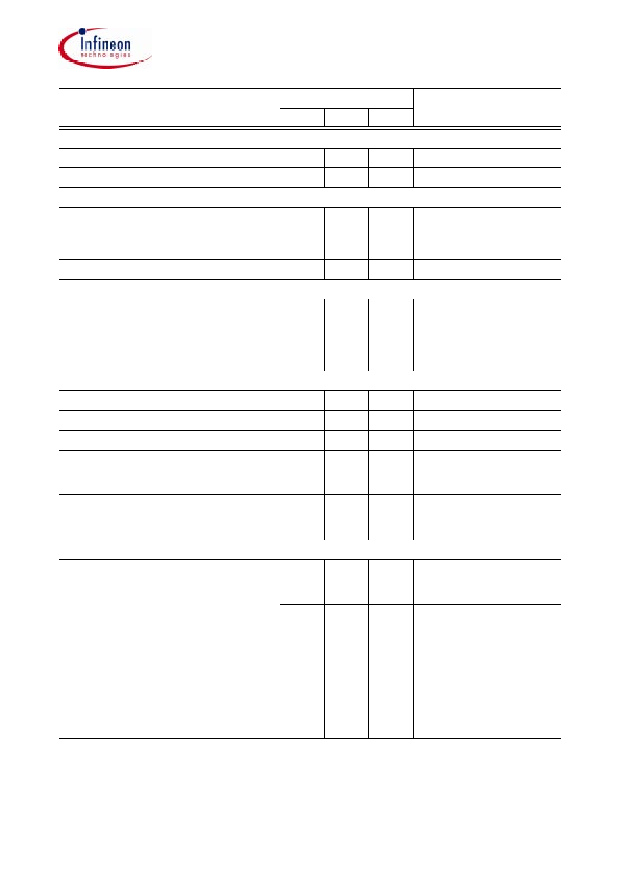
10 Operating Range
Within the operational range the IC operates as described in the circuit description.
The AC / DC characteristic limits are not guaranteed.
Parameter
Symbol
(Name)
Limit Values
Unit
Test Conditions
min
max
Supply voltage (digital)
V
VD
4.5
5.5
V
Supply voltage (analog)
V
VA
7.2
13.2
V
Input frequency range of
converter mixer
f
MIXIN
5
10
MHz
Input frequency range of
sound IF amplifier
f
IF
10
12
MHz
VCO frequency
f
VCO
29
42
MHz
Ambient temperature
T
A
0
70
∞
C
Data Sheet
TDA6170X
Semiconductor Group
17
21.7.99
11 Electrical Characteristics
AC / DC characteristics involve the spread of values guaranteed in the specified supply voltage and ambient
temperature range. Typical characteristics are the median of the production.
Parameter
Symbol
Limit Values
Unit
Test conditions
min
typ
max
Power Supply
Current consumption V
digital
I
VD
30
40
50
mA
Current consumption V
analog
I
VA
30
40
50
mA
Mixer
Mixer input voltage
V
MIXIN(rms)
200
mV
Mixer output current
I
MIXOUT
4
6
8
mA
Input impedance
R
MIXIN
3.5
k
Output frequency range
f
MIXOUT
10
10.7
11.5
MHz
Mixer gain
G
MIX
2
3
4
dB
RL = 100
Charge pump
Phase detector charge current
I
PD
32
50
75
µ
A
I
Phase detector charge current
I
PD
160
250
360
µ
A
5I
repetition time of charge pump
pulses
t
50
µ
s
VCO
Frequency range VCO
f
VCO
29
43
MHz
VCO frequency
f
VCO
35.5
MHz
V
PD
= 2.5V
VCO sensitivity
S
VCO
-16
MHz/V
Cyrstal oscillator (4 MHz)
crystal oscillator frequency
f
xtal
4
MHz
resonance resistance of crystal
R
xtal
60
W
parallel capacitance of crystal
C
xtal
4.5
10
pF
input current from external source I
i
50
µ
A
Sound IF
Sound IF input resistance
R
IF
260
330
400
W
Input frequency range
f
IF
10
11.5
MHz
Input sensitivity
V
IF(rms)
0.3
1
mV
S/N(A) > 40 dB;
f
IF
= 10.7 MHz;
f = 27 kHz;
f
mod
= 1 kHz
AM rejection
a
AM
45
dB
f
IF
= 10.7 MHz;
V
IF
= 5 to 100mV;
f
mod
= 30%
Data Sheet
TDA6170X
Semiconductor Group
18
21.7.99
FM PLL demodulators
free-running frequency
f
cco
10.6
MHz
lock range of PLL
f
CCO
10
11.5
MHz
Expander
Pre volume control range
PV
2.5
-3.5
3
-3
3.5
-2.5
dB
PVL = 000
PVL = 111
Control resolution
V
0.6
0.8
1
dB
Low-pass filter response
16
20
24
kHz
AF Switch and Volume Control
Max. external input voltage
V
EXT(rms)
2
V
Volume control range
V
-1
-12
0
-14
1
-16
dB
VL = 000
VL = 111
Control resolution
V
1.6
2
2.4
dB
Output Buffer
Output DC level
V
AF
3.6
V
Output resistance
R
AF
100
125
150
W
total harmonic distortion
THD
0.01
0.2
%
signal to noise ratio
S/N (A)
80
dB
A-weighted
V
EXT
= 500 mV
rms
Control Byte = 110
crosstalk between channels
L/R
;
R/L
80
dB
V
EXT
= 2 V
rms
f = 1 kHz
Control Byte = 110
Overall performance
Input voltage
V
MIXIN
0.5
1
mV
S/N > 40 dB
f = 27kHz,
Control Byte = 000
1.5
3
mV
S/N > 40 dB
f = 50kHz,
Control Byte = 011
Output voltage
V
AF
400
500
600
mV
f = 27kHz,
f
mod
= 1kHz,
Control Byte = 000
400
500
600
mV
f = 50kHz,
f
mod
= 1kHz,
Control Byte = 011
Parameter
Symbol
Limit Values
Unit
Test conditions
min
typ
max
Data Sheet
TDA6170X
Semiconductor Group
19
21.7.99
total harmonic distortion
THD
0.2
0.5
%
V
MIXIN
> 2 mV
f = 27kHz,
f
mod
= 1kHz,
Control Byte = 000
0.2
0.5
%
V
MIXIN
> 2 mV
f = 50kHz,
f
mod
= 1kHz,
Control Byte = 011
signal to noise ratio
S/N
70
75
dB
A-weighted,
f = 27kHz,
f
mod
= 1kHz,
Control Byte = 000
Mute attenuation
a
MUTE
75
90
dB
Control Byte = 111
I
2
C-Bus Interface
LOW level input voltage for both
SDA and SCL
V
IL
-0.5
1.5
V
HIGH level input voltage for both
SDA and SCL
V
IH
3
V
VD
+
0.5
V
Hysteresis of Schmitt trigger
inputs
V
hys
0.2
V
Pulse width of spikes which must
be suppressed by the input filters
t
SP
50
ns
LOW level output voltage (open
collector)
V
OL1
V
OL2
0
0
0.4
0.6
V
3 mA sink current
6 mA sink current
Output fall time from
V
IHmin
to V
ILmax
with a bus
capacitance from 10 pF to 400 pF
t
OF
20 +
0.1C
b
250
ns
Input current for both SDA + SCL
I
i
-10
10
µ
A
SCL clock frequency
f
SCL
0
400
kHz
Bus free time between a STOP
and START condition
t
BUF
1.3
µ
s
Hold time (repeated) START con-
dition. After this period, the first
clock pulse is generated
t
HD,STA
0.6
µ
s
LOW period of the SCL clock
t
LOW
1.3
µ
s
HIGH period of the SCL clock
t
HIGH
0.6
µ
s
Set-up time for repeated START
condition
t
SU,DAT
0.6
µ
s
Data hold time:
for I
2
C-bus devices
t
HD,DAT
0
0.9
µ
s
Data set-up time
t
SU,DAT
100
ns
Rise time of both SDA + SCL
t
R
20 +
0.1C
b
300
ns
Parameter
Symbol
Limit Values
Unit
Test conditions
min
typ
max

Data Sheet
TDA6170X
Semiconductor Group
20
21.7.99
Fall time of both SDA + SCL
t
F
20 +
0.1C
b
300
ns
Set-up time for STOP condition
t
SU,STO
0.6
µ
s
Capacitive load for each bus line
C
b
400
pF
Parameter
Symbol
Limit Values
Unit
Test conditions
min
typ
max
Data Sheet
TDA6170X
Semiconductor Group
21
21.7.99
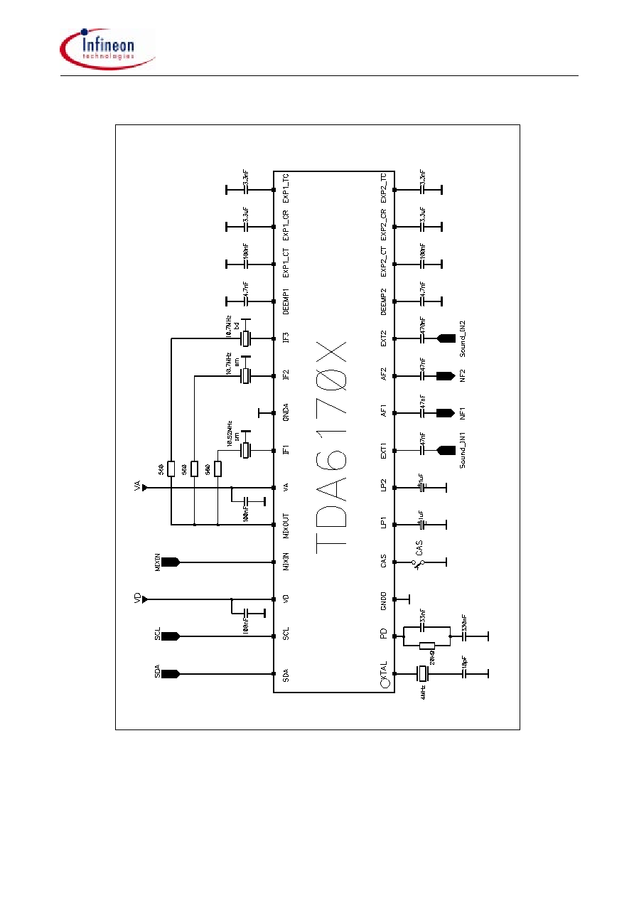
12 Application Circuit
Data Sheet
TDA6170X
Semiconductor Group
22
21.7.99
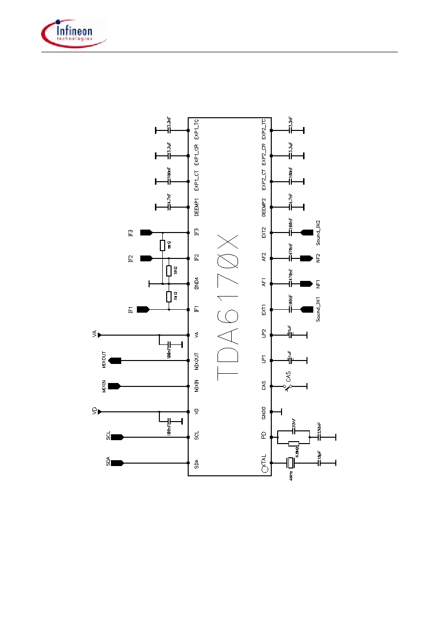
13 Test circuit
Data Sheet
TDA6170X
Semiconductor Group
23
21.7.99
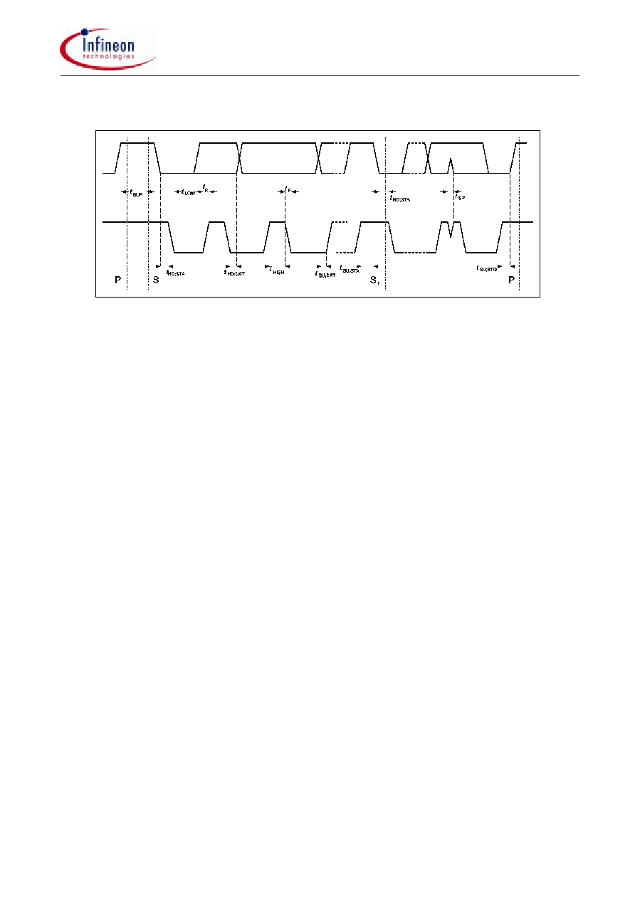
14 Diagrams
14.1 I
2
C-Bus Timing