Semiconductor Group
FEATURES
∑ Compliant with existing standards
∑ Compact integrated transceiver unit with
≠ MQW laser diode transmitter
≠ InGaAs PIN photodiode receiver
≠ Duplex SC receptacle
∑ Class 1 FDA and IEC laser safety compliant
∑ FDA Accession No. 9520890-03
∑ Single power supply (+5 V)
∑ Loss of optical signal indicator
∑ Integrated clock recovery module (PLL)
∑ PECL differential inputs and outputs
∑ Process plug included
∑ Wave solderable and washable with process
plug inserted
Absolute Maximum Ratings
Exceeding any one of these values may destroy the device
immediately.
Package Power Dissipation
(1)
..................................................... Tbd W
Supply Voltage (V
&&
≠V
((
)................................................................. 6 V
Data Input Levels.................................................................. V
((
to V
&&
Differential Data Input Voltage ........................................ ≠2.5 V to 2.5 V
Operating Case Temperature ............................................ 0
∞
C to 70
∞
C
Storage Ambient Temperature .......................................≠40
∞
C to 85
∞
C
Soldering Conditions Temp/Time
(MIL-STD 883 C Method 2003) ........................................ 250
∞
C/5.5s
Note
1. For V
88
≠V
@@
(min., max.). 50% duty cycle. The supply current does not
include the load drive current of the receiver output. Add max. 45 mA for the
three outputs. Load is 50
to VCC≠ 2 V.
DESCRIPTION
The Siemens single mode ATM transceiver complies with the ATM
Forum's
Network Compatible ATM for Local Network Applications
document and ANSI's
Broadband ISDN - Customer Installation Inter-
faces, Physical Media Dependent Specification, T1.646-1995.
ATM was developed to facilitate solutions in multimedia applications
and real time transmission. The data rate is scalable, and the ATM proto-
col is the basis of the broadband public networks being standardized in
the International Telecommunications Union (ITU), the former Interna-
tional Telegraph and Telephone Consultative Committee (CCITT). ATM
can also be used in local private applications.
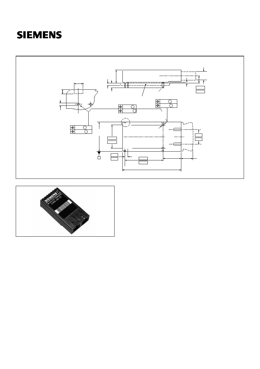
V23806-A84-C51
Single Mode 622 MBd ATM 2x9 Transceiver
with Clock Recovery
(1.5
±
0.1
)
.06
±
.004
(8.6 max.)
.338 max.
(0.75
±
0.1)
.030
±
.004
6.375
.251
Optical
Centerline
PC board
(11.5 max.)
.453 max.
(
4
±
0.2
)
.158
±
.008
(2) .080
(0.73
±
0.1)
.028
±
.004
(
0.45
±
0.1
)
.0175
±
.004
(25.4
±
0.1
)
1
±
.004
20.32
.800
123456789
18
17
1
6
1
5
14
13
12
1
1
1
0
33.02
1.3
(15.88
±
0.5
)
.625
±
.020
(52 max.)
2.048 max.
2.54
.100
0.2 M
.008 M
0.3 M
.012 M
A
A
0.3 M
.012 M
A
A
20x
2x
Z
18x
DUPLEX
SC
RECEPTACLE
View Z
(Lead cross section
and standoff size)
PC board
thickness
qqqqqqqqq
qqqqqqqqq
(1.4
-0.05
)
.055
-.002
A
Top view
12.7
.500
(11 max.)
.433 max.
Rx
Tx
a. isolated stud pins, connected to GND on request
(a)
Dimensions in (mm) inches
JULY 1998

V23806-A84-C51 Single Mode 622 MBd ATM 2x9 Transceiver w/Clock Recovery
2
Semiconductor Group
This Siemens single mode ATM transceiver is a single unit com-
prised of a transmitter, a receiver, a clock recovery module, and
an SC receptacle. This design frees the customer from many
alignment and PC board layout concerns. The module is
designed for low cost WAN applications. It can be used as the
network end device interface in workstations, servers, and stor-
age devices, and in a broad range of network devices such as
bridges, routers, and intelligent hubs, and wide area ATM
switches.
This transceiver operates at 622.080 Mbits per second from a
single power supply (+5 Volt). The differential data inputs, data
outputs, clock outputs and signal detect output are PECL
compatible.
Functional Description of 2x9 Pin Row Transceiver
This transceiver is designed to transmit serial data via single
mode cable.
Functional Diagram
The receiver component converts the optical serial data into
PECL compatible electrical data (RxD and RxDn). It provides also
a recovered in-phase clock and clock not signal. The Signal
Detect (SD, active high) shows whether an optical signal is
present. If no optical input signal is present the receiver data out-
puts are switched to static low level (RD=low, RDnot=high).
The transmitter part converts electrical PECL compatible serial
data (TxD and TxDn) into optical serial data. It contains a laser
driver circuit that drives the modulation and bias current of the
laser diode. The currents are controlled by a power control circuit
to guarantee constant output power of the laser over tempera-
ture and aging. The power control uses the output of the monitor
PIN diode (mechanically built into the laser coupling unit) as a
controlling signal, to prevent the laser power from exceeding the
operating limits.
The laser can be switched off with a logical high signal on the
Transmitter Disable pin (TxDIS). The PWRMON pin shows a
voltage reflecting the optical power output. The bias current is
monitored on the BIASMON pins. Both signals can be used to
supervise the function of the module.
The signal TXALM (optional) indicates an increasing of the optical
output power of more than 2dB. Aging control is possible using
the bias monitor output (BIASMON). The module has an inte-
grated shutdown function that switches the laser off in the event
of an internal failure.
Laser
Driver
Laser
Power
Control
Receiver
SD
PLL
Clock
TXALM
TxD
RxD
RxDn
BIASMON≠
BIASMON+
TxDn
Laser
Coupling Unit
RX
Coupling Unit
e/o
o/e
o/e
TxDIS
PWRMON
3k
3k
10
Single
Mode
Fiber
Automatic
Shut-Down
TECHNICAL DATA
The electro-optical characteristics described in the follow-
ing tables are valid only for use under the recommended
operating conditions.
Recommended Operating Conditions
Note
1. For V
88
≠V
@@
(min., max.). 50% duty cycle. The supply current does
not include the load drive current of the receiver output. Add max.
75 mA for the five outputs. Load is 50
to V
88
≠ 2 V.
Transmitter Electro-Optical Characteristics
Notes
1. Transmitter meets ANSI T1E1.2, SONET OC-12, and ITU G.957
mask patterns.
2. Laser power is shut down if power supply is below V
UC√
and
switched on if power supply is above V
UC√
after t
S@T
. The supervi-
sory circuit can be reset by switching TxDis from high to low.
Parameter
Symbol
Min.
Typ. Max.
Units
Case Temperature
T
&
0
70
∞
C
Power Supply Voltage
V
&&
≠V
((
4.75
5
5.25
V
Supply Current
(1)
I
&&
230
300
mA
Transmitter
Data Input High Voltage
V
,+
≠V
&&
≠1165
≠880
mV
Data Input Low Voltage
V
,/
≠V
&&
≠1810
≠1475
Input Data Rise/Fall
Time, 10%≠90%
t
R
, t
F
0.4
1.3
ns
TxDis Input High Voltage
V
7,+
2
V
TxDis Input Low Voltage
V
7,/
0.8
TxDis Input High Current
V
7,+
0.8
mA
TxDis Input Low Current
V
7,/
≠1
TxALM Output
High Voltage
V
72+
3.2
V
TxALM Output
Low Voltage
V
72/
0.7
TxALM Output
High Current
I
72+
≠3
mA
TxALM Output
Low Current
I
72/
3
Receiver
Output Current
I
O
25
mA
Input Center Wavelength
C
1260
1360
nm
Transmitter
Symbol Min.
Typ.
Max.
Units
Output Power (Average) P
2
≠15.0
≠11.0
≠8.0
dBm
Center Wavelength
C
1274
1356
nm
Spectral Width, RMS
2.5
Output Rise Time,
20%≠80%
t
5
240
700
ps
Output Fall Time,
20%≠80%
t
)
240
700
Extinction Ratio
(Dynamic)
ER
8.2
dB
Eye Diagram
(1)
ED
Reset Threshold for
TxV
&&
�
V
7+
4.25
4.38
4.5
V
Reset Active Time Out
(2)
t
5(6
140
240
560
ms
V23806-A84-C51 Single Mode 622 MBd ATM 2x9 Transceiver w/Clock Recovery
3
Semiconductor Group
Regulatory Compliance
Receiver Electro-Optical Characteristics
Notes
1. Minimum average optical power at which the BER is less than
1 x 10
E-10
. Measured with a 2
23
-1 NRZ PRBS as recommended by
ANSI T1E1.2, SONET OC-12, and ITU G.957.
2. An increase in optical power above the specified level will cause the
SIGNAL DETECT to switch from a Low state to a High state.
3. A decrease in optical power below the specified level will cause the
SIGNAL DETECT to switch from a High state to a Low state.
4. PECL compatible. Load is 50
into V
88
≠2 V. Measured under DC
conditions at 25
∞
C. For dynamic measurements a tolerance of
50 mV should be added. V
88
=+5 V.
5. In accordance with ITU G. 958 and 825. Details to be specified.
Feature
Standard
Comments
Electrostatic
Discharge (ESD)
to the Electrical Pins
MIL-STD 883C
Method 3015.4
Class 1 (>1000 V)
Immunity:
Electrostatic
Discharge (ESD)
to the Duplex SC
Receptacle
EN 61000-4-2
IEC 1000-4-2
Discharges of
±
15kV
with an air discharge
probe on the receptacle
cause no damage.
Immunity:
Radio Frequency
Electromagnetic
Field
EN 61000-4-3
IEC 1000-4-3
With a field strength of
10 V/m rms, noise
frequency ranges from
10 MHz to 1 GHz. No
effect on transceiver
performance between
the specification limits.
Emission:
Electromagnetic
Interference (EMI)
FCC Class B
EN 55022 Class B
CISPR 22
Noise frequency range:
30 MHz to 1 GHz
Receiver
Symbol
Min.
Typ. Max.
Units
Sensitivity
(Average Power)
(1)
P
,1
≠33
≠29
dBm
Saturation
(Average Power)
P
6$7
≠8.0
≠3.0
Signal Detect
Assert Level
(2)
P
6'$
≠29
Signal Detect
Deassert Level
(3)
P
6''
44
Signal Detect
Hysteresis
P
6'$
≠
P
6''
1.5
dB
Signal Detect
Assert Time
t
$66
1
ms
Signal Detect
Deassert Time
t
'$6
5
PECL Output
Low Voltage
(4)
V
OL
≠
V
&&
≠1950
≠1630
mV
PECL Output
High Voltage
(4)
V
OH
≠
V
&&
≠1025
≠735
Output Data, Rise/Fall
Time, 10%≠90%
t
5
, t
)
1
ns
Output SD,
Rise/Fall Time
40
Jitter Tolerance
(5)
J
7R
UI
Jitter Transfer
(5)
J
7U
Jitter Generation
(5)
J
*H
LASER SAFETY
This single mode ATM transceiver is a Class 1 laser product. It
complies with IEC 825-1 and FDA 21 CFR 1040.10 and 1040.11.
The transceiver must be operated under recommended operat-
ing conditions.
Caution
The use of optical instruments with this product will
increase eye hazard!
General Restrictions
Classification is valid only if the module is operated within the
specified temperature and voltage limits. The system using the
module must provide power supply protection that guarantees
that the system power source will cease to provide power if the
maximum recommended operation limit or more is detected on
the +5V at the power source. The case temperature of the
module must be in the temperature range given in the recom-
mended operating limits. These limits guarantee the laser safety.
Usage Restrictions
The optical ports of the modules shall be terminated with an
optical connector or with a dust plug.
Note
Failure to adhere to the above restrictions could result in a modification
that is considered an act of "manufacturing," and will require, under
law, recertification of the modified product with the U.S. Food and Drug
Administration (ref. 21 CFR 1040.10 (i)).
Laser Data
Required Labels
Laser Emission
Wavelength
1300 nm
Total output power (as defined by IEC: 50 mm aperture
at 10 cm distance)
2 mW
Total output power (as defined by FDA: 7 mm aperture
at 20 cm distance)
180
µ
W
Beam divergence
4
∞
Class 1 Laser Product
IEC
Complies with 21 CFR
1040.10 and 1040.11
FDA
Indication of laser
aperture and beam

Siemens Microelectronics, Inc. ∑ Optoelectronics Division ∑ 19000 Homestead Road ∑ Cupertino, CA 95014 USA
Siemens Semiconductor Group ∑ Fiber Optics ∑ Wernerwerkdamm 16 ∑ Berlin D-13623, Germany
Siemens K.K. ∑ Fiber Optics ∑ Takanawa Park Tower ∑ 20-14, Higashi-Gotanda, 3-Chome ∑ Shinagawa-ku ∑ Tokyo 141, Japan
www.smi.siemens.com/opto/fo/fo.html (USA) ∑ www.siemens.de/Semiconductor/products/37/376.htm (Germany)
Pin Description
APPLICATION NOTE
Single Mode 622 MBd ATM 2x9 Transceiver
* Recommended choke is Siemens Matsushita B78108-S1153-K or B78148-S1153-K (QPLQ=60, max. DC resistance =0.6
).
Pin Name
Level
Pin#
Description
NC
1≠2
Pin not connected
RxCLKn
Clock Output Not
PECL Output
3
Inverted receiver clock output
RxCLK
Clock Output
4
Receiver clock output
Bias Mon
Bias Monitor
Analog Voltage
Bias Mon ≠
Bias Mon +
5
6
This output shows an analog voltage that is proportional to the laser bias
current. Use this output to check proper laser operation and for end of life
indications. Limit: Bias Current I
%,$6
<60 mA
TxDis
Tx Disable/Enable
TTL-Input active
7
A falling slope switches the laser on.
A rising slope switches the laser off. High >3.5 V; Low <0.8 V
Tx Alm
(optional)
Tx+2dB Alarm
TTL Output
active
8
A high level on this output indicates an increase in optical operating power
output of+2 dB.
Pwr Mon
Power Monitor
Analog Voltage
9
This output shows an analog voltage that is proportional to the light output.
This output can be used for laser safety functions.
Output Voltage Vmon=1.2
±
0.2 V, Source Resistance R
6
=100 k
TxV
((
Tx Ground
Power Supply
10
Negative power supply, normally ground
TxD
Tx Input Data
PECL Input
11
Transmitter input data
TxDn
12
Inverted transmitter input data
TxV
&&
Tx +5 V
Power Supply
13
Positive power supply, +5 V
RxV
&&
Rx +5 V
Power Supply
14
SD
RX Signal Detect
PECL Output
active high
15
A high level on this output shows that an optical signal is applied to the
optical input.
RxDn
Rx Output Data
PECL Output
16
Inverted receiver output data
RxD
17
Receiver output data
RxV
((
Rx Ground
Power Supply
18
Negative power supply, normally ground
3 k
3 k
10
V
CC
-Tx
V
CC
GND
GND
GND
L1
L2
C1
C3
C2
very short
very short
R1
0
R1
1
Top View
GND
GND
GND
GND
GND
GND
Transceiver
V
CC
-Rx
V
CC
-Tx
very short
very short
very short
very short
R1
R3
R2
R4
R7
R8
R9
9
10
18
1
RD
SD
RDN
TXD
TXDN
BiasMon+
TxDis
TxALM
CLK
CLKN
TxMonit
BiasMon≠
V
CC
-Rx
R6
R5
Termination behind
AC coupling
ECL/PECL
Interf
ace
50R
50R
50R
GND
GND
ECL Termination
50
to V
EE
50
to V
EL
C1/C3 = 4.7
µ
F optional
C2 = 4.7
µ
F
L1 = 15
µ
H
L2 = 4.7
µ
H
R1/3/5 = 68
R2/4/6 = 185
R7 = 500
R8/9/10/11 = 200
The power supply filtering is required for good EMI performance. Use
short tracks from the inductor L1/L2 to the module V
&&
≠RX/V
&&
≠TX.
A GND plane under the module is required for good EMI and
sensitivity performance. Studs should be connected to this
GND plane. The transceiver contains an automatic shutdown circuit.
Reset is only possible when the power is turned off, and then on again
(V
&&
TX=0 V), or by disabling the transmitter with TxDIS and enabling it
after at least 500 ms. The receiver data signals should be terminated
with 50
at the far end. 200
terminations should be placed very
close to the receiver data pins in combination with AC coupling.