
Fiber Optics
MARCH 2000
5 V
V23806-A84-C6
Single Mode 155 MBd ATM/SDH/SONET 2x9 Transceiver
with Rx Monitor
FEATURES
∑ Compliant with ATM, SONET OC-3, SDH STM-1
∑ Compact integrated transceiver unit with
≠ MQW laser diode transmitter
≠ InGaAs PIN photodiode receiver
≠ Duplex SC receptacle
∑ Class 1 FDA and IEC laser safety compliant
∑ FDA Accession No. 9520890-08
∑ Single power supply (5 V)
∑ Signal detect indicator
∑ PECL differential inputs and outputs
∑ Process plug included
∑ Wave solderable and washable with process
plug inserted
∑ Analog Rx power monitor output
∑ Industry multisource 2x9 footprint
∑ For distances of up to 15 km on single mode fiber
Absolute Maximum Ratings
Exceeding any one of these values may destroy the device
immediately.
Package Power Dissipation
(1)
............................................ 1.5 W
Supply Voltage (V
CC
≠V
EE
) ...................................................... 6 V
Data Input Levels...........................................................V
CC
+0.5
Differential Data Input Voltage ............................................ 2.5 V
Operating Case Temperature.................................. 0
∞
C to 70
∞
C
Storage Ambient Temperature ............................≠40
∞
C to 85
∞
C
Soldering Conditions Temp/Time
(MIL-STD 883 C Method 2003) ............................. 250
∞
C/5.5s
Note
1. For
V
CC
≠V
EE
(min., max.). 50% duty cycle. The supply current does
not include the load drive current of the receiver output. Add max.
45 mA for the three outputs. Load is 50
to VCC≠ 2 V.
(1.5
±
0.1
)
.06
±
.004
(8.6 max)
.338 max
(0.75
±
0.1
)
.030
±
.004
6.375
.251
Optical
Centerline
PC board
(11.5 max)
.453 max.
(2) .080
(0.73
±
0.1)
.028
±
.004
(
0.45
±
0.1)
.0175
±
.004
(25.4
±
0.1
)
1
±
.004
20.32
33.02
1.3
(15.88
±
0.5
)
.625
±
.020
(52 max)
2.048 max
2.54
.100
20x
2x
Z
18x
DUPLEX
SC
RECEPTACLE
View Z
(Lead cross section
and standoff size)
PC board
thickness
(1.4
-0.05
)
.055
-.002
A
12.7
(11 max)
.433 max
Rx
Tx
.500
Top view
123456789
18
17
16
15
1
4
1
3
1
2
1
1
1
0
qqqqqqqqq
qqqqqqqqq
M
M
0.2
.008
M
M
0.3
.012
(4
±
0.2
)
.158
±
.008
A
A
M
M
0.3
.012
A
A
(4
±
0.2
)
.158
±
.008
Dimensions in (mm) inches
Fiber Optics
V23806-A84-C6, Single Mode 155 MBd ATM/SDH/SONET 2x9 Trx w/Rx Monitor, 5 V
2
DESCRIPTION
The Infineon single mode ATM transceiver complies with the
ATM Forum's Network Compatible ATM for Local Network
Applications document and ANSI's Broadband ISDN -
Customer Installation Interfaces, Physical Media Dependent
Specification, T1.646-1995, Bellcore-SONET OC-3/IR-1 and
ITU-T G.957 STM-1/S.1.1.
ATM was developed to facilitate solutions in multimedia appli-
cations and real time transmission. The data rate is scalable,
and the ATM protocol is the basis of the broadband public net-
works being standardized in the International Telecommunica-
tions Union (ITU), the former International Telegraph and
Telephone Consultative Committee (CCITT). ATM can also be
used in local private applications.
This Infineon single mode ATM transceiver is a single unit com-
prised of a transmitter, a receiver, and an SC receptacle. This
design frees the customer from many alignment and PC board
layout concerns. The module is designed for low cost WAN
applications. It can be used as the network end device interface
in workstations, servers, and storage devices, and in a broad
range of network devices such as bridges, routers, and intelli-
gent hubs, and wide area ATM switches.
This transceiver operates at 155.52 Mbit/s from a single power
supply (+5 V). The differential data inputs, data outputs and sig-
nal detect output are PECL compatible.
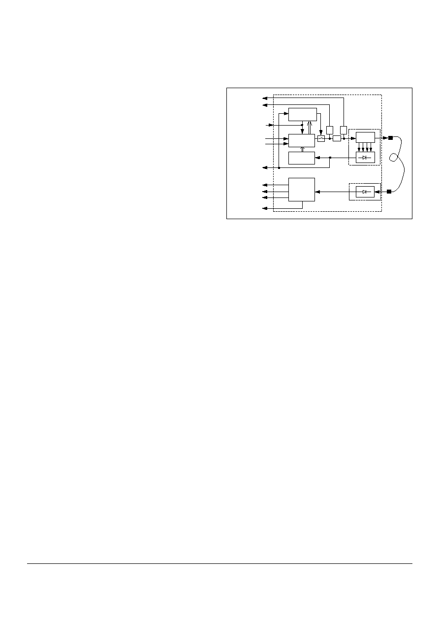
Functional Description
This transceiver is designed to transmit serial data via single
mode cable.
Functional Diagram
The receiver component converts the optical serial data into
PECL compatible electrical data (RxD and RxDn). The Signal
Detect (SD, active high) shows whether an optical signal is
present
(1)
.
This transceiver offers the advantage of an analog Rx power
monitor (RxPMON) that can prove and control link status,
including transmission distances and security of the connec-
tion. This output shows an analog voltage that is proportional to
the light input within the range of -20 dBm to -30 dBm.
The transmitter part converts electrical PECL compatible serial
data (TxD and TxDn) into optical serial data. It contains a laser
driver circuit that drives the modulation and bias current of the
laser diode. The currents are controlled by a power control cir-
cuit to guarantee constant output power of the laser over tem-
perature and aging.
The power control uses the output of the monitor PIN diode
(mechanically built into the laser coupling unit) as a controlling
signal, to prevent the laser power from exceeding the operating
limits.
The laser can be switched off with a high signal on the Trans-
mitter Disable pin (TxDis). The TxPMon pin shows a voltage
reflecting the optical power output. The bias current is moni-
tored on the BIASMON pins. Both signals can be used to super-
vise the function of the module.
Aging control is possible using the bias monitor output (BIAS-
MON). The module has an integrated shutdown function that
switches the laser off in the event of an internal failure.
The transceiver contains a supervisory circuit to control the
power supply. This circuit generates an internal reset signal
whenever the supply voltage drops below the reset threshold.
It keeps the reset signal active for at least 15 milliseconds after
the voltage has risen above the reset threshold. During this
time the laser is inactive.
Note
1. We recommend to switch off the transmitter supply (V
CC
-Tx) if no
transmitter input data is applied.
Laser
Driver
Laser
Power
Control
Receiver
SD
RxPMon
TxD
RxD
RxDn
BIASMON-
BIASMON+
TxDn
Laser
Coupling Unit
RX
Coupling Unit
e/o
o/e
o/e
TxDIS
TxPMon
3k
3k
10
Single
Mode
Fiber
Automatic
Shut-Down

Fiber Optics
V23806-A84-C6, Single Mode 155 MBd ATM/SDH/SONET 2x9 Trx w/Rx Monitor, 5 V
3
TECHNICAL DATA
The electro-optical characteristics described in the following
tables are valid only for use under the recommended operating
conditions.
Recommended Operating Conditions
Note
1. For
V
CC
≠V
EE
(min., max.). 50% duty cycle. The supply current does
not include the load drive current of the receiver output. Add max.
45 mA for the three outputs. Load is 50
to V
CC
≠ 2 V.
Transmitter Electro-Optical Characteristics
Notes
1. Transmitter meets ANSI T1E1.2, SONET OC-3, and ITU-T G.957
mask patterns.
2. Laser power is shut down if power supply is below V
TH
and
switched on if power supply is above V
TH
after t
RES
. The supervi-
sory circuit can be reset by switching TxDis from high to low.
Receiver Electro-Optical Characteristics
Notes
1. Minimum average optical power at which the BER is less than
1 x 10
-10
. Measured with a 2
23
-1 NRZ PRBS as recommended by
ANSI T1E1.2, SONET OC-3, and ITU-T G.957.
2. An increase in optical power of data signal above the specified level
will cause the SIGNAL DETECT to switch from a Low state to a High
state.
3. A decrease in optical power of data signal below the specified level
will cause the SIGNAL DETECT to switch from a High state to a Low
state.
4. PECL compatible. Load is 50
into V
CC
≠2 V. Measured under DC
conditions at 25
∞
C. For dynamic measurements a tolerance of
50 mV should be added. V
CC
=+5 V.
Parameter
Symbol
Min.
Typ. Max.
Units
Case Temperature
T
C
0
70
∞
C
Power Supply
Voltage
V
CC
≠V
EE
4.75
5.0
5.25
V
Supply
Current
(1)
I
CC
230
250
mA
Transmitter
Data Input High Voltage
V
IH
≠V
CC
≠1165
≠880
mV
Data Input Low Voltage
V
IL
≠V
CC
≠1810
≠1475
Input Data Rise/Fall Time,
10%≠90%
tR, tF
0.4
1.3
ns
TxDis Input High Voltage
V
TIH
2.0
V
TxDis Input Low Voltage
V
TIL
0.8
Receiver
Output Current
I
O
25
mA
Input Center Wavelength
C
1260
1360
nm
Transmitter
Symbol
Min.
Typ.
Max.
Units
Output Power (Average) P
O
≠15.0
≠11.0 ≠8.0
dBm
Center Wavelength
C
1274
1356
nm
Spectral Width, RMS
l
2.5
Output Rise/Fall Time,
20%≠80%
t
R
,
t
F
0.4
ns
Extinction Ratio
(Dynamic)
ER
8.2
12
dB
Eye Diagram
(1)
ED
Reset Threshold
for TxV
CC
(2)
V
TH
2.85
2.93
3.0
V
Reset Active
Time Out
(2)
t
RES
15
22
35
ms
Receiver
Symbol
Min.
Typ. Max.
Units
Sensitivity
(Average Power)
(1)
P
IN
≠34
≠29
dBm
Saturation
(Average Power)
P
SAT
≠8.0
≠3.0
Signal Detect
Assert Level
(2)
P
SDA
≠38
≠34
Signal Detect
Deassert Level
(3)
P
SDD
≠44
≠40
Signal Detect
Hysteresis
P
SDA
≠
P
SDD
2
dB
Signal Detect
Assert Time
t
ASS
1
ms
Signal Detect
Deassert Time
t
DAS
5
PECL Output
Low Voltage
(4)
V
OL
≠
V
CC
≠1950
≠1630
mV
PECL Output
High Voltage
(4)
V
OH
≠
V
CC
≠1025
≠735
Output Data, Rise/Fall
Time, 20%≠80%
t
R
, t
F
0.7
1
ns
Output SD,
Rise/Fall Time
40

Fiber Optics
V23806-A84-C6, Single Mode 155 MBd ATM/SDH/SONET 2x9 Trx w/Rx Monitor, 5 V
4
Pin Description
Regulatory Compliance
Pin Name
Level
Pin#
Description
NC
1≠4
Pin not connected
Bias Mon
Bias Monitor
Analog Voltage
Bias Mon ≠
Bias Mon +
5
6
This output shows an analog voltage that is proportional to the laser bias
current. Use this output to check proper laser operation and for end of life
indications. Limit: Bias Current I
BIAS
<60 mA
I
BIAS
=
TxDis
Tx Disable/Enable
TTL-Input
7
A low signal switches the laser on.
A high signal switches the laser off.
RxPMon
Rx Power Monitor
Analog Voltage
8
This output shows an analog voltage that is proportional to the light input.
Output voltage RxPMon = 2.5 V (typical) at ≠20 dBm opt. input signal and
RxPMon = 0.3 V (typical) at ≠30 dBm opt. input signal.
Source Resistance R
S
= 300 k
.
TxPMon
Tx Power Monitor
Analog Voltage
9
This output shows an analog voltage that is proportional to the light output.
This output can be used for laser safety functions.
Output Voltage Vmon = 1.2, Source Resistance R
S
= 100 k
TxV
EE
Tx Ground
Power Supply
10
Negative power supply, normally ground
TxD
Tx Input Data
PECL Input
11
Transmitter input data
TxDn
12
Inverted transmitter input data
TxV
CC
Tx +5 V
Power Supply
13
Positive power supply, +5 V
RxV
CC
Rx +5 V
Power Supply
14
SD
Rx Signal Detect
PECL Output
active high
15
A high level on this output shows that optical data is applied to the
optical input.
RxDn
Rx Output Data
PECL Output
16
Inverted receiver output data
RxD
17
Receiver output data
RxV
EE
Rx Ground
Power Supply
18
Negative power supply, normally ground
Stud Pin
Mech. Support
S1/2
Not connected
Feature
Standard
Comments
Electrostatic Discharge (ESD)
to the Electrical Pins
MIL-STD 883C
Method 3015.4
Class 1 (>1000 V)
Immunity:
Electrostatic Discharge (ESD) to the
Duplex SC Receptacle
EN 61000-4-2
IEC 61000-4-2
Discharges of
±
15kV with an air discharge probe on the receptacle cause no
damage.
Immunity:
Radio Frequency
Electromagnetic Field
EN 61000-4-3
IEC 61000-4-3
With a field strength of 3 V/m rms, noise frequency ranges from 10 MHz to
1 GHz. No effect on transceiver performance between the specification limits.
Emission:
Electromagnetic Interference (EMI)
FCC Class B
EN 55022 Class B
CISPR 22
Noise frequency range: 30 MHz to 1 GHz
3 k
3 k
10
U
10

Fiber Optics
V23806-A84-C6, Single Mode 155 MBd ATM/SDH/SONET 2x9 Trx w/Rx Monitor, 5 V
5
EYE SAFETY
This laser based single mode transceiver is a Class 1 product. It
complies with IEC 60825-1 and FDA 21 CFR 1040.10 and
1040.11.
To meet laser safety requirements the transceiver shall be oper-
ated within the Absolute Maximum Ratings.
Caution
All adjustments have been made at the factory prior to ship-
ment of the devices. No maintenance or alteration to the
device is required.
Tampering with or modifying the performance of the device
will result in voided product warranty.
Note
Failure to adhere to the above restrictions could result in a modifica-
tion that is considered an act of "manufacturing," and will require,
under law, recertification of the modified product with the U.S. Food
and Drug Administration (ref. 21 CFR 1040.10 (i)).
Laser Data
Required Labels
Laser Emission
Wavelength
1300 nm
Total output power (as defined by IEC: 50 mm aperture
at 10 cm distance)
less than
2 mW
Total output power (as defined by FDA: 7 mm aperture
at 20 cm distance)
less than
180
µ
W
Beam divergence
4
∞
Class 1 Laser Product
IEC
Complies with 21 CFR
1040.10 and 1040.11
FDA
Indication of laser
aperture and beam

Published by Infineon Technologies AG
©
Infineon Technologies AG 1999
All Rights Reserved
Attention please!
The information herein is given to describe certain components and shall not be
considered as warranted characteristics.
Terms of delivery and rights to technical change reserved.
We hereby disclaim any and all warranties, including but not limited to warranties
of non-infringement, regarding circuits, descriptions and charts stated herein.
Infineon Technologies is an approved CECC manufacturer.
Information
For further information on technology, delivery terms and conditions and prices
please contact the Infineon Technologies offices or our Infineon Technologies
Representatives worldwide - see our webpage at
www.infineon.com/fiberoptics
Warnings
Due to technical requirements components may contain dangerous substances.
For information on the types in question please contact your Infineon Technologies
offices.
Infineon Technologies Components may only be used in life-support devices or
systems with the express written approval of Infineon Technologies, if a failure of
such components can reasonably be expected to cause the failure of that
life-support device or system, or to affect the safety or effectiveness of that device
or system. Life support devices or systems are intended to be implanted in the
human body, or to support and/or maintain and sustain and/or protect human life.
If they fail, it is reasonable to assume that the health of the user or other persons
may be endangered.
Infineon Technologies AG ∑ Fiber Optics ∑ Wernerwerkdamm 16 ∑ Berlin D-13623, Germany
Infineon Technologies, Inc. ∑ Fiber Optics ∑ 1730 North First Street ∑ San Jose, CA 95112, USA
Infineon Technologies K.K. ∑ Fiber Optics ∑ Takanawa Park Tower ∑ 20-14, Higashi-Gotanda, 3-chome, Shinagawa-ku ∑ Tokyo 141, Japan
APPLICATION NOTE
Single Mode 155 MBd ATM 2x9 Transceiver
* Recommended choke is Siemens Matsushita B78108-S1153-K or B78148-S1153-K (Qmin=60, max. DC resistance =0.6
).
The power supply filtering is recommended for good EMI per-
formance. Use short tracks from the inductor L1/L2 to the mod-
ule V
CC
-Rx/V
CC
-Tx. We recommend a V
EE
plane under the
module for getting good EMI performance. The transceiver con-
tains an automatic shutdown circuit. Reset is only possible
when the power is turned off, and then on again (V
CC
Tx = 0 V).
The receiver data signals should be terminated with 50
at the
far end. Terminations should be placed very close to the
receiver data pins in combination with AC coupling.
RxPMon
TxPMon
TxDis
BIASMON+
BIASMON
Top View
Transceiver
V
EE
V
EE
V
EE
V
EE
V
EE
V
EE
V
EE
V
EE
V
EE
V
EE
V
EE
S2
S1
R1
R3
R5
R7
R2
R4
R6
R9
R8
TxD
TxDN
RxD
RxDN
SD
L1
L2
V
CC
V
CC
C1
C2
C3
C4
V
CC
-Tx
V
CC
-Rx
10
18
1
9
C1/C3 = 4.7 µF optional
C2/4
= 4.7 µF
L1/2
= 15 µH (L2 optional)*
R1/3
= 68
R2/4
= 185
R5/7
= 82
R6/8
= 127
R9
= 510