 | –≠–ª–µ–∫—Ç—Ä–æ–Ω–Ω—ã–π –∫–æ–º–ø–æ–Ω–µ–Ω—Ç: IA186ES | –°–∫–∞—á–∞—Ç—å:  PDF PDF  ZIP ZIP |

IA21140AF Preliminary
Data Sheet
PCI FAST ETHERNET LAN CONTROLLER
Copyright
©
2001
ENG210010110-00
www.innovasic.com
innov
ASIC
Customer Support:
The End of Obsolescence
TM
Page 1 of 19
1-888-824-4184
Features
∑
Form, Fit and Function Compatible with the DEC
TM
21140AF
∑
Available in 144 Pin PQFP Package
∑
Integrated Ethernet controller with PCI bus interface
∑
Supports 10 Mb/s and 10/100 Mb/s network interface
∑
PCS and scrambler/descrambler circuitry on chip
∑
Supports multiple PCI features:
- Unlimited PCI burst
- PCI read multiple
- PCI write and invalidate
- PCI read line
- PCI 5.0V and 3.3V environments
∑
Multiple interrupt sources
∑
Contains two independent 3K FIFOs to minimize external memory additions
∑
Provides sleep or snooze low-power modes
∑
Interfaces with MicroWire
TM
Serial ROM
∑
Provides a JTAG test port with boundary scan function
∑
Complies with IEEE 802.3, ANSI 8802-3, and Ethernet standards
The IA21140AF is a "plug-and-play" drop-in replacement for the original IC. innov
ASIC
produces
replacement ICs using its MILES
TM
, or Managed IC Lifetime Extension System, cloning technology. This
technology produces replacement ICs far more complex than "emulation" while ensuring they are compatible
with the original IC. MILES
TM
captures the design of a clone so it can be produced even as silicon
technology advances. MILES
TM
also verifies the clone against the original IC so that even the
"undocumented features" are duplicated. This data sheet documents all necessary engineering information
about the IA21140AF including functional and I/O descriptions, electrical characteristics, and applicable
timing.
innov
ASIC

IA21140AF Preliminary
Data Sheet
PCI FAST ETHERNET LAN CONTROLLER
Copyright
©
2001
ENG210010110-00
www.innovasic.com
innov
ASIC
Customer Support:
The End of Obsolescence
TM
Page 2 of 19
1-888-824-4184
Package Pinout
1
2
3
4
5
6
7
8
9
10
11
12
13
14
15
16
17
18
19
20
21
22
23
24
25
26
27
28
29
30
31
32
33
34
35
36
100
99
98
97
96
95
94
93
92
91
90
89
88
87
86
85
84
83
82
81
80
79
78
77
76
75
74
73
101
102
103
104
105
106
107
108
3
7
3
8
3
9
4
0
4
1
4
2
4
3
4
4
4
5
4
6
4
7
4
8
4
9
5
0
5
1
5
2
5
3
5
4
5
5
5
6
5
7
5
8
5
9
6
0
6
1
6
2
6
3
6
4
6
5
6
6
6
7
6
8
6
9
7
0
7
1
7
2
1
0
9
1
1
0
1
1
1
1
1
2
1
1
3
1
1
4
1
1
5
1
1
6
1
1
7
1
1
8
1
1
9
1
2
0
1
2
1
1
2
2
1
2
3
1
2
4
1
2
5
1
2
6
1
2
7
1
2
8
1
2
9
1
3
0
1
3
1
1
3
2
1
3
3
1
3
4
1
3
5
1
3
6
1
3
7
1
3
8
1
3
9
1
4
0
1
4
1
1
4
2
1
4
3
1
4
4
IA21140AF
int_n
rst_n
vdd
vss
pci_clk
vdd
vss
gnt_n
req_n
ad[31]
ad[30]
vss
ad[29]
ad[28]
ad[27]
vss
ad[26]
vdd
ad[25]
ad[24]
c_be_n[3]
idsel
vss
ad[23]
ad[22]
ad[21]
ad[20]
vdd
ad[19]
ad[18]
vdd
vss
vss
ad[17]
ad[16]
vss
c_be_n[2]
frame_n
irdy_n
trdy_n
devsel_n
stop_n
perr_n
serr_n
par
c_be_n[1]
ad[15]
vss
vdd
vss
ad[14]
ad[13]
vss
ad[12]
ad[11]
vdd
ad[10]
ad[9]
vss
ad[8]
c_be_n[0]
ad[7]
ad[6]
vss
ad[5] ad[4]
vdd
ad[3]
ad[2]
vss
ad[1]
ad[0]
vss
vdd
mii_mdc
mii_mdio
nc
br_a[1]
br_ce_n
br_a[0]
br_ad[7]
vss
vdd
br_ad[6]
br_ad[5]
br_ad[4]
br_ad[3]
br_ad[2]
br_ad[1]
br_ad[0]
vss
gep[7]
gep[6]
gep[5]
gep[4]
vdd
vss
gep[3]
gep[2]
gep[1]
gep[0]
sr_cs
sr_ck
sr_di
sr_do
vdd
vss
vdd_clamp
tdi
tms
tck
srl_txen srl_tclk
srl_txd
srl_rxen
srl_rxd
srl_clsn
mii_srl
tdo
srl_rclk
sym_txd[4]
vdd
vss
mii_sym_txen
mii_sym_txd[3]
mii_sym_txd[2]
mii_sym_txd[1]
mii_sym_txd[0]
sym_link mii_sym_tclk
rcv_match
vdd
vss
sym_rxd[4]
mii_sym_rxd[3]
mii_sym_rxd[2]
mii_sym_rxd[1] mii_sym_rxd[0]
mii_sym_rclk
mii_crs
mii_clsn
mii_dv
mii_err
sd

IA21140AF Preliminary
Data Sheet
PCI FAST ETHERNET LAN CONTROLLER
Copyright
©
2001
ENG210010110-00
www.innovasic.com
innov
ASIC
Customer Support:
The End of Obsolescence
TM
Page 3 of 19
1-888-824-4184
Description
The innov
ASIC
IA21140AF Fast Ethernet LAN controller provides a direct interface connection to
the PCI (Peripheral Component Interface) bus. It interfaces with the PCI bus by using on-chip
control and status registers (CSR's), and a shared CPU memory area. The memory is initialized once
during setup to minimize CPU overhead during normal operation. Large receive and transmit
FIFO's are contained on-chip so no additional on board memory is required. The IA21140AF
includes two on chip direct memory access (DMA) controllers with programmable burst size
providing for low CPU utilization. A PCI clock frequency from dc to 33 MHz (20-33 MHz for
operational network interface) is supported. Two network ports are supported. A serial standard 7-
wire 10-Mbps port (SRL) and a media independent interface/symbol 10/100-Mbps port
(MII/SYM). The 10 Mbps implements a direct interface to the external 10 Mbps front-end decoder
(ENDEC). The 10/100 Mbps port supports two modes. The first is a 100BASE-X physical coding
sublayer (PCS). The second is a full implementation of the MII standard. The IA21140AF functions
in a full-duplex environment for either network port.
IA21140AF Preliminary
Data Sheet
PCI FAST ETHERNET LAN CONTROLLER
Copyright
©
2001
ENG210010110-00
www.innovasic.com
innov
ASIC
Customer Support:
The End of Obsolescence
TM
Page 4 of 19
1-888-824-4184
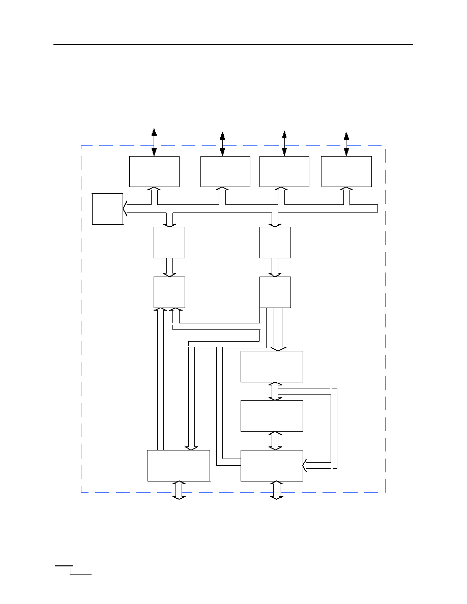
System Block Diagram
This block below illustrates the major functions of the IA21140AF.
PCI
Interface
Boot
ROM
Port
Serial
ROM
Port
General-
Purpose
Register
Board
Control
Signals
Boot ROM/
External
Register
Serial
ROM
PCI
32
32
8
Rx
FIFO
Tx
FIFO
RxM
TxM
10 Mb/s
Physical
Coding
Sublayer
Scrambler/
Descrambler
MII/SYM
Interface
Serial
Interface
10 Mb/s or 100 Mb/s
DMA
32
32
32
16
16
4
4
4
1
1
4

IA21140AF Preliminary
Data Sheet
PCI FAST ETHERNET LAN CONTROLLER
Copyright
©
2001
ENG210010110-00
www.innovasic.com
innov
ASIC
Customer Support:
The End of Obsolescence
TM
Page 5 of 19
1-888-824-4184
I/O Description
The following section provides a functional description of the I/O pins on the IA21140AF.
NAME
Type
Description
Vdd
P
3.3 volt input supply voltage.
Vdd_clamp
P
5.0 volt reference for 5.0 volt signaling environments and 3.3 volt reference
for 3.3 volt signaling environments.
Vss
P
Ground Pin
ad[31:0]
I/O
The PCI address and data lines are multiplexed on the same PCI pins. During
the first clock cycle of a transaction, the 32 bits contain an address and during
subsequent clock cycles, they contain data. Both read and write bursts are
supported in master operation only. Big or Little Indian byte ordering can be
used.
br_a[1:0]
O
Address line bit 0 also carries in two consecutive address cycles (bits 16 and
17) in a 256KB configuration. Bit 1 also latches the boot ROM address and
control lines via two external latches.
br_ad[7:0]
I/O
In the first of two consecutive address cycles, these multiplexed lines contain
the boot ROM address bits [7:2], oe_n, and we_n. The second cycle contains
boot ROM address bits [15:8]. Bits 7 through 0 contain data during the data
cycle. These lines are used to carry data to and from the external register.
br_ce_n
O
Enable pin for the Boot ROM or an external register. Pin has an internal 5 k O
pull-up resistor.
c_be_n[3:0]
I/O
Bus command and byte enable are multiplexed on the same PCI pins. These
bits provide the bus command during the address phase of the transaction.
They provide the byte enable during the data phase. Byte enable determines
which byte lines carry valid data. Bit 0 coincides with byte 0. Bit 1 coincides
with byte 1, etc.
devsel_n
I/O
Indicates that the driving device has decoded its address as the target of the
current access. As an input, determines whether a device on the bus has
been selected.
frame_n
I/O
The IA21140AF bus master asserts this signal to indicate the beginning and
duration of a bus transaction access. Data transfer continues while this signal
is asserted. Deasserting this signal indicates the transaction is in the final
phase.
gep[7:0]
I/O
These pins can be configured by software to perform either input or output
functions for system specific applications.
gnt_n
I
Indicates to the IA21140AF that access to the bus has been granted.
Idsel
I
Used as a chip select by the host to indicate configuration read and write
cycles.
int_n
O/D
When one of the appropriate bits in CSR5 gets set, interrupt request gets
asserted if the corresponding mask bit in CSR7 is not set. If more than one
interrupt bit in CSR5 is set and all input bits are not cleared, interrupt request
gets deasserted for one clock cycle. Interrupt request gets deasserted by
writing a "1" into the appropriate CSR5 bit. This pin must be pulled up by an
external resistor.