
Page 1 of 19
IA2910A
Preliminary
Data Sheet
Microprogram Controller
Copyright
©
1999, InnovASIC Inc.
Customer Specific IC Solutions
FEATURES
∑
Form, Fit, and Function Compatible with the AMD
TM
Am2910A
∑
Packaging options available: 40 Pin Plastic or Ceramic DIP, 44 Pin Plastic
Leaded Chip Carrier
∑
Twelve Bits Wide
∑
Internal Loop Counter
∑
Four Address Sources
- push/pop stack counter
- internal holding register
- microprogram counter
- branch address bus
∑
9 Word Deep Stack Register
- push/pop control for nesting subroutines
∑
16 Sequence Control Microinstructions
∑
Output Enable controls 3 Branch Address Sources
The IA2910A uses innov
ASIC
's innovative new f
3
Program to provide industry with parts that
other vendors have declared obsolete. By specifying parts through this program a customer is
assured of never having a component become obsolete again. This data sheet assumes the original
part has been designed in, and so provides a summary of capabilities only. For new designs contact
innov
ASIC
for more detailed information.
AMD is a trademark of Advanced Micro Devices, Inc.
(6)
PLn
(1)
YOUT4
(2)
DIN4
(3)
YOUT5
(4)
DIN5
(5)
VECTn
(7)
MAPn
(8)
I3
(9)
I2
(10)
VCC
(11)
I1
(12)
I0
(13)
CCENn
(14)
40 Pin DIP
IA2910A
CIN
CLK
VDD
OEn
(20)
YOUT7
(15)
RLDn
(16)
FULLn
(17)
DIN6
(18)
YOUT6
(19)
DIN7
(21)
(22)
(23)
(24)
YOUT8
DIN8
(40)
(39)
(38)
(37)
(36)
(35)
(34)
(33)
(32)
(31)
(30)
(29)
(28)
(27)
(26)
(25)
CCn
YOUT9
DIN9
YOUT10
DIN10
YOUT11
DIN11
DIN0
YOUT0
DIN1
YOUT1
DIN2
YOUT2
DIN3
YOUT3
FULLn
44 Pin LCC
IA2910A
(12)
I1
(7)
PLn
(8)
MAPn
(9)
I3
(10)
I2
(11)
VCC
(13)
I0
(14)
CCENn
(15)
CCn
(16)
RLDn
(17)
N.C.
YOUT1
VDD
CLK
CIN
YOUT0
DIN0
YOUT6
DIN6
(6)
(5)
(4)
(3)
(2)
(1)
(44)
(43)
(42)
DIN2
(41)
YOUT2
(40)
DIN1
VECTn
N. C.
(34)
(39)
(38)
(37)
(36)
(35)
(33)
(32)
(31)
(30)
(29)
(18)
(19)
(20)
(21)
(22)
(23)
(24)
(25)
(26)
(27)
(28)
DIN3
YOUT3
DIN4
YOUT4
DIN5
YOUT5
YOUT7
DIN7
YOUT8
DIN8
YOUT9
DIN9
YOUT10
DIN10
DIN11
YOUT11
OEn
N. C.
N. C.
Page 2 of 19
IA2910A
Preliminary
Data Sheet
Microprogram Controller
Copyright
©
1999, InnovASIC Inc.
Customer Specific IC Solutions
The IA2910A is a form, fit and function compatible part to the AMD 2910A microprogram
controller. The IA2910A is an address controller which will sequence through a series of
microinstructions contained in a ROM or PROM. There are four sources of addresses from which
the IA2910A may select. The first is a direct data bus (DIN) input, which is straightforward. The
second is an internal address register. This register contains data loaded during a previous
microinstruction. The third source is a program counter register, which generally contains the
previous address incremented by one. The final source of addresses is a nine word deep stack
register which gives the capability to execute nested subroutine linkages. All internal registers are
clocked on the rising edge of the clock input (CLK). An OEn input enables the YOUT output bus
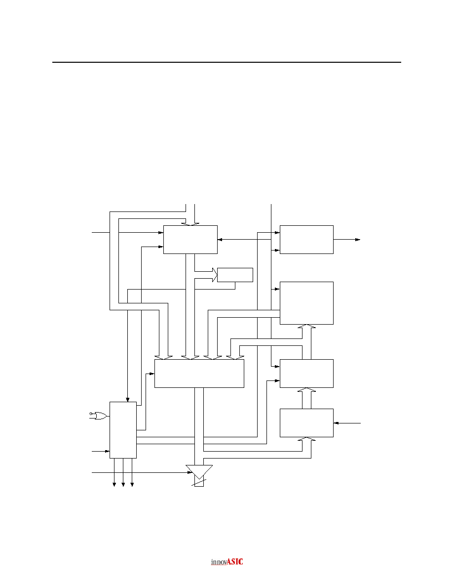
to be tri-stated. A block diagram is shown in Figure 1.
Functional Block Diagram
Figure 1
Register/Counter
Instruction
PLA
Zero
Detector
Microprogram
counter-register
Mux
Incrementer
9 word X 12 Bit
Stack
Stack Pointer
12
YOUT
RLDn
DIN
CCn
CCENn
I(3:0)
PLn
MAPn
VECTn
CIN
CLK
FULLn
SELECT
R=0
DECREMENT/
HOLD/LOAD
PUSH/POP/
HOLD/CLEAR
CLEAR/COUNT

Page 3 of 19
IA2910A
Preliminary
Data Sheet
Microprogram Controller
Copyright
©
1999, InnovASIC Inc.
Customer Specific IC Solutions
Functional Overview
The IA2910A is a 0.8 µm CMOS microprogram controller intended for use in high-speed
microprocessor applications. It allows addressing of up to 4K words of microprogram
.
The controller contains a four-input mux that is used to select either the register/counter, direct
data input, microprogram counter, or stack as the source of the next microinstruction address.
The register/counter consists of 12 D-type, edge-triggered flip-flops, with a common clock enable.
When its load control, RLDn, is LOW, new data is loaded on a positive clock transition. A few
instructions include load; in most systems, these instructions will be sufficient, simplifying the
microcode. The output of the register/counter is available to the mux as a source for the next
microinstruction address. The direct input furnishes a source of data for loading the
register/counter.
The IA2910A contains a microprogram counter that is composed of a 12-bit incrementer followed
by a 12-bit register. The counter can be used in either of two ways. When the carry-in to the
incrementer is HIGH, the microprogram register is loaded on the next clock cycle with the current
YOUT output word plus one. Sequential microinstructions are thus executed. When the carry-in is
LOW, the incrementer passes the YOUT output word unmodified so that the counter is reloaded
with the same YOUT word on the next clock cycle. The same microinstruction is thus executed
any number of times.
The third source for the mux is the direct DIN input. This source is used for branching.
The fourth source available at the mux input is a 9-word by 12-bit stack (file). The stack is used to
provide return address linkage when executing microsubroutines or loops. The stack contains a
built-in stack pointer (SP) which always points to the last file word written. This allows stack
reference operations (looping) to be performed without a pop.
The stack pointer operates as an up/down counter. During microinstructions 1, 4, and 5, the
PUSH operation may occur. This causes the stack pointer to increment and the file to be written
with the required return linkage. On the cycle following the PUSH, the return data is at the new
location pointed to by the stack pointer.
During five microinstructions, a POP operation may occur. The stack pointer decrements at the
next rising clock edge following a POP, effectively removing old information from the top of the
stack.
The stack pointer linkage is such that any sequence of pushes, pops, or stack references can be
achieved. At RESET (Instruction 0), the depth of nesting becomes zero. For each PUSH, the
nesting depth increases by one; for each POP, the depth decreases by one. The depth can grow to
nine. After a depth of nine is reached, FULLn goes LOW. Any further PUSHes onto a full stack
overwrite information at the top of the stack, but leave the stack pointer unchanged. This
operation will usually destroy useful information and is normally avoided. A POP from an empty
stack may place non-meaningful data on the YOUT outputs, but is otherwise safe. The stack

Page 4 of 19
IA2910A
Preliminary
Data Sheet
Microprogram Controller
Copyright
©
1999, InnovASIC Inc.
Customer Specific IC Solutions
pointer remains at zero whenever a POP is attempted from a stack already empty.
The register/counter is operated during three microinstructions (8, 9, and 15) as a 12-bit down
counter, with result = zero available as a microinstruction branch test criterion. This provides
efficient iteration of microinstructions. The register/counter is arranged such that if it is preloaded
with a number N and then used as a loop termination counter, the sequence will be executed
exactly N + 1 times. During instruction 15, a three-way branch under combined control of the
loop counter and the condition code is available.
The device provides three-state YOUT outputs. These can be particularly useful in designs
requiring automatic checkout of the processor. The microprogram controller outputs can be
forced into the high-impedance state, and pre-programmed sequences of microinstructions can be
executed via external access to the address lines.

Page 5 of 19
IA2910A
Preliminary
Data Sheet
Microprogram Controller
Copyright
©
1999, InnovASIC Inc.
Customer Specific IC Solutions
I/O Signal Description
Table 1 below describes the I/O characteristics for each signal on the IC. The signal names
correspond to the signal names on the pinout diagrams provided.
Table 1
Symbol
Type
Description
CLK
I
Clock Input - Clock source for address register, microprogram
counter register, and stack file.
I(3:0)
I
Active high instruction bits. Selects instruction to be executed by the
IA2910A.
CCn
I
Active low. Condition code. Used as test criterion, pass is low on
CCn.
CCENn
I
Active low. Condition code enable. When set high, CCn is ignored
and the IA2910A operates as it CCn were a low.
RLDn
I
Active low. Clock enable to address register, allows loading of
register/counter regardless of instruction or condition.
OEn
I
Active low. Output enable, when high tri-states the output bus
YOUT.
CIN
I
Active high. Carry in signal to the incrementer.
FULLn
O
Active low. Indicates there are nine items on the stack.
DIN(11:0)
I
Active high. Data bus input to the multiplexer.
YOUT(11:0)
O
Active high. Data bus output from the IA2910A.
PLn
O
Active low. Pipeline address enable. Selects source number one
(usually pipeline register) as direct input source.
MAPn
O
Active low. Map address enable. Selects source number two (usually
mapping PROM or PLA) as direct input source.
VECTn
O
Active low. Vector address enable. Selects source number three
(usually interrupt starting address) as direct input source.
Theory of Operation
Table 2 shows the result of each instruction in controlling the mux which determines the YOUT
outputs, and in controlling the three enable signals PLn, MAPn, and VECTn. The effect on the
register/counter and the stack after the next positive-going clock edge is also shown. The mux
determines which internal source drives the YOUT outputs. The value loaded into the counter is