IA6805E2
Data Sheet
Microprocessor Unit
As of Production Version 00
Copyright
©
2002
ENG21108140100
www.innovasic.com
innov
ASIC
Customer Support:
The End of Obsolescence
TM
Page 1 of 31
1-888-824-4184
FEATURES
∑
Form, Fit, and Function Compatible with the Harris
©
CDP6805E2CE and
Motorola
©
MC146805E2
∑
Internal 8-bit Timer with 7-Bit
Programmable Prescaler
∑
On-chip Clock
∑
Memory Mapped I/O
∑
Versatile Interrupt Handling
∑
True Bit Manipulation
∑
Bit Test and Branch Instruction
∑
Vectored Interrupts
∑
Power-saving STOP and WAIT Modes
∑
Fully Static Operation
∑
112 Bytes of RAM
The IA6805E2 is a "plug-and-play" drop-in replacement for the original IC. innov
ASIC
produces
replacement ICs using its MILES
TM
, or Managed IC Lifetime Extension System, cloning technology. This
technology produces replacement ICs far more complex than "emulation" while ensuring they are compatible
with the original IC. MILES
TM
captures the design of a clone so it can be produced even as silicon
technology advances. MILES
TM
also verifies the clone against the original IC so that even the
"undocumented features" are duplicated. This data sheet documents all necessary engineering information
about the IA6805E2 including functional and I/O descriptions, electrical characteristics, and applicable
timing.
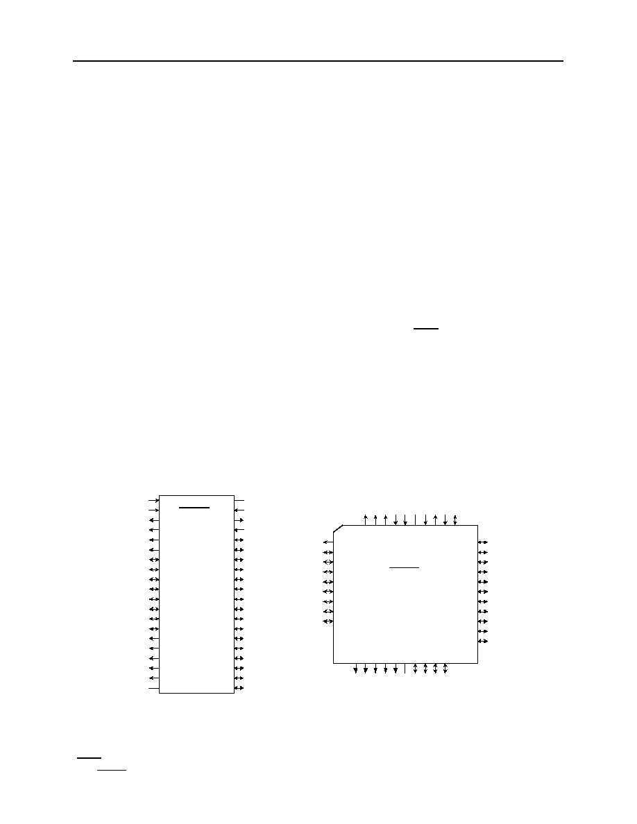
Package Pinout
A12
NC
(6)
AS
(1)
RESET_N
(2)
IRQ_N
(3)
LI
(4)
DS
(5)
RW_N
(7)
PA7
(8)
(9)
PA5
(10)
(11)
(12)
PA2
(13)
PA1
(14)
40 Pin DIP
IA6805E2
PB4
PB5
PB6
PB7
(20)
VSS
(15)
A12
(16)
A11
(17)
A10
(18)
A9
(19)
A8
(21)
(22)
(23)
(24)
B6
B7
(40)
(39)
(38)
(37)
(36)
(35)
(34)
(33)
(32)
(31)
(30)
(29)
(28)
(27)
(26)
(25)
PA0
B4
B5
B2
B3
B0
B1
PB2
PB3
PB0
PB1
OSC2
TIMER
VDD
OSC1
PA6
PA4
PA3
RW_N
NC
B2
44 Pin LCC
IA6805E2
(12)
PA3
(7)
AS
(8)
PA7
(9)
PA6
(10)
PA5
(11)
PA4
(13)
PA2
(14)
PA1
(15)
PA0
(16)
NC
(17)
NC
PB1
PB7
PB6
PB5
PB3
PB2
A10
A11
(6)
(5)
(4)
(3)
(2)
(1)
(44)
(43)
(42)
OSC2
(41)
TIMER
(40)
PB0
(34)
(39)
(38)
(37)
(36)
(35)
(33)
(32)
(31)
(30)
(29)
(18)
(19)
(20)
(21)
(22)
(23)
(24)
(25)
(26)
(27)
(28)
VDD
OSC1
IRQ_N
RESET_N
DS
LI
A8
A9
B7
VSS
B5
B6
B4
B3
B1
B0
PB4

IA6805E2
Data Sheet
Microprocessor Unit
As of Production Version 00
Copyright
©
2002
ENG21108140100
www.innovasic.com
innov
ASIC
Customer Support:
The End of Obsolescence
TM
Page 3 of 31
1-888-824-4184
Table 1
I/O Signal Description
The table below describes the I/O characteristics for each signal on the IC. The signal names
correspond to the signal names on the pinout diagrams provided.
S I G N A L N A M E
I / O
D E S C R I P T I O N
V
D D
a n d V
S S
( P o w e r a n d G r o u n d )
N / A
S o u r c e : T h e s e t w o p i n s p r o v i d e p o w e r t o t h e c h i p . V
D D
p r o v i d e s + 5 v o l t s ( ± 0 . 5 ) p o w e r
a n d V
S S
i s g r o u n d .
R E S E T _ n
( R e s e t )
I
T T L : I n p u t pin t h a t c a n b e u s e d t o r e s e t t h e M P U ' s i n t e r n a l s t a t e b y p u l l i n g t h e r e s e t _ n
p i n l o w .
I R Q _ n
( I n t e r r u p t R e q u e s t )
I
T T L : I n p u t pin t h a t i s l e v e l a n d e d g e s e n s i t i v e . C a n b e u s e d t o r e q u e s t a n i n t e r r u p t
s e q u e n c e .
L I
( L o a d I n s t r u c t i o n )
O
T T L w i t h s l e w rate c o n t r o l : O u t p u t pin u s e d to i n d i c a t e t h a t a n e x t o p c o d e f e t c h i s in
p r o g r e s s . U s e d o n l y f o r c e r t a i n d e b u g g i n g a n d t e s t s y s t e m s . N o t c o n n e c t e d in n o r m a l
o p e r a t i o n . O v e r l a p s D a t a S t r o b e ( D S ) s i g n a l . T h i s o u t p u t i s c a p a b l e o f d r i v i n g o n e
s t a n d a r d T T L l o a d a n d 5 0 p F .
D S
( D a t a S t r o b e )
O
T T L w i t h s l e w r a t e c o n t r o l : O u t p u t p i n u s e d to t r a n s f e r d a t a t o o r f r o m a p e r i p h e r a l o r
m e m o r y . D S o c c u r s a n y t i m e t h e M P U d o e s a d a t a r e a d o r w r i t e a n d d u r i n g d a t a t r a n s f e r
t o o r f r o m i n t e r n a l m e m o r y . D S is a v a i l a b l e a t f
O S C
˜
5 w h e n t h e M P U is n o t in t h e W A I T
o r S T O P m o d e . T h i s o u t p u t i s c a p a b l e o f d r i v i n g o n e s t a n d a r d T T L l o a d a n d 1 3 0 p F .
R W _ n
( R e a d / W r i t e )
O
T T L w i t h s l e w rate c o n t r o l : O u t p u t pin u s e d to i n d i c a t e t h e d i r e c t i o n o f d a t a t r a n s f e r
f r o m i n t e r n a l m e m o r y , I / O r e g i s t e r s , a n d e x t e r n a l p e r i p h e r a l d e v i c e s a n d m e m o r i e s .
I n d i c a t e s t o a s e l e c t e d p e r i p h e r a l w h e t h e r t h e M P U i s to r e a d ( R W _ n h i g h ) o r w r i t e
( R W _ n l o w ) d a t a o n t h e n e x t d a t a s t r o b e . T h i s o u t p u t i s c a p a b l e o f d r i v i n g o n e s t a n d a r d
T T L l o a d a n d 1 3 0 p F .
A S
( A d d r e s s S t r o b e )
O
T T L w i t h s l e w rate c o n t r o l : O u t p u t s t r o b e u s e d to i n d i c a t e t h e p r e s e n c e o f a n a d d r e s s
o n t h e 8 - b i t m u l t i p l e x e d b u s . T h e A S l i n e i s u s e d to d e m u l t i p l e x t h e e i g h t l e a s t s i g n i f i c a n t
a d d r e s s b i t s f r o m t h e d a t a b u s . A S i s a v a i l a b l e a t f
O S C
˜
5 w h e n t h e M P U i s n o t in t h e
W A I T o r S T O P m o d e s . T h i s o u t p u t i s c a p a b l e o f d r i v i n g o n e s t a n d a r d T T L l o a d a n d
1 3 0 p F .
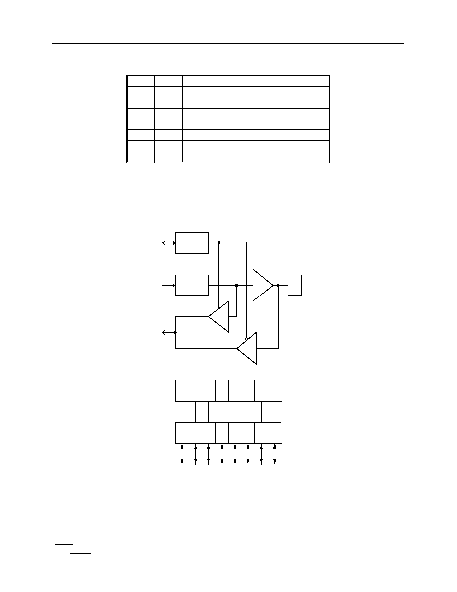
P A 0 - P A 7 / P B 0 - P B 7
( I n p u t / O u t p u t L i n e s )
I / O
T T L w i t h s l e w rate c o n t r o l : T h e s e 1 6 l i n e s c o n s t i t u t e I n p u t / O u t p u t p o r t s A a n d B .
E a c h l i n e is i n d i v i d u a l l y p r o g r a m m e d to b e e i t h e r a n i n p u t o r o u t p u t u n d e r s o f t w a r e
c o n t r o l o f t h e D a t a D i r e c t i o n R e g i s t e r ( D D R ) a s s h o w n b e l o w in T a b l e 1 a n d F i g u r e 2 .
T h e p o r t I / O is p r o g r a m m e d b y w r i t i n g t h e c o r r e s p o n d i n g b i t in t h e D D R to a " 1 " f o r
o u t p u t a n d a " 0 " f o r i n p u t . In t h e o u t p u t m o d e t h e b i t s a r e l a t c h e d a n d a p p e a r o n t h e
c o r r e s p o n d i n g o u t p u t p i n s . All t h e D D R ' s a r e i n i t i a l i z e d to a " 0 " o n r e s e t . T h e o u t p u t
p o r t r e g i s t e r s a r e n o t i n i t i a l i z e d o n r e s e t . E a c h o u t p u t i s c a p a b l e o f d r i v i n g o n e s t a n d a r d
T T L l o a d a n d 5 0 p F .
A 8 - A 1 2
( H i g h O r d e r A d d r e s s L i n e s )
O
T T L w i t h s l e w r a t e c o n t r o l :
T h e s e f i v e o u t p u t s c o n s t i t u t e t h e h i g h e r o r d e r n o n -
m u l t i p l e x e d a d d r e s s l i n e s . E a c h o u t p u t i s c a p a b l e o f d r i v i n g o n e s t a n d a r d T T L l o a d a n d
1 3 0 p F .
B 0 - B 7
( A d d r e s s / D a t a B u s )
I / O
T T L w i t h s l e w rate c o n t r o l :
T h e s e b i - d i r e c t i o n a l l i n e s c o n s t i t u t e t h e l o w e r o r d e r
a d d r e s s e s a n d d a t a . T h e s e l i n e s a r e m u l t i p l e x e d w i t h a d d r e s s p r e s e n t a t a d d r e s s s t r o b e
t i m e a n d d a t a p r e s e n t a t d a t a s t r o b e t i m e . W h e n in t h e d a t a m o d e , t h e s e l i n e s a r e b i -
d i r e c t i o n a l , t r a n s f e r r i n g d a t a t o a n d f r o m m e m o r y a n d p e r i p h e r a l d e v i c e s a s i n d i c a t e d b y
t h e R W _ n p i n . A s o u t p u t s , t h e s e l i n e s a r e c a p a b l e o f d r i v i n g o n e s t a n d a r d T T L l o a d a n d
1 3 0 p F .
T i m e r
I
T T L : I n p u t u s e d t o c o n t r o l t h e i n t e r n a l t i m e r / c o u n t e r c i r c u i t r y .
O S C 1 , O S C 2
( S y s t e m C l o c k )
T T L O s c i l l a t o r i n p u t / o u t p u t : T h e s e p i n s p r o v i d e c o n t r o l i n p u t f o r t h e o n - c h i p c l o c k
o s c i l l a t o r c i r c u i t s . E i t h e r a c r y s t a l o r e x t e r n a l c l o c k i s c o n n e c t e d to t h e s e p i n s to p r o v i d e
a s y s t e m
c l o c k .
T h e c r y s t a l c o n n e c t i o n i s s h o w n in F i g u r e 3 . T h e O S C 1 to b u s
t r a n s i t i o n s f o r s y s t e m d e s i g n s u s i n g o s c i l l a t o r s s l o w e r t h a n 5 M H z i s s h o w n i n F i g u r e 4 .
C r y s t a l
T h e c i r c u i t s h o w n in F i g u r e 3 is r e c o m m e n d e d w h e n u s i n g a c r y s t a l . A n e x t e r n a l C M O S
o s c i l l a t o r is r e c o m m e n d e d w h e n u s i n g c r y s t a l s o u t s i d e t h e s p e c i f i e d r a n g e s . T o m i n i m i z e
o u t p u t d i s t o r t i o n a n d s t a r t - u p s t a b i l i z a t i o n t i m e , t h e c r y s t a l a n d c o m p o n e n t s s h o u l d b e
m o u n t e d a s c l o s e t o t h e i n p u t p i n s a s p o s s i b l e .
E x t e r n a l C l o c k
W h e n a n e x t e r n a l c l o c k i s u s e d , i t s h o u l d b e a p p l i e d to t h e O S C 1 i n p u t w i t h t h e O S C 2
i n p u t n o t c o n n e c t e d , a s s h o w n i n F i g u r e 3 .
I / O